minDiffNetSpacing
spacings( ( minDiffNetSpacingtx_layerf_spacing)
) ;spacings
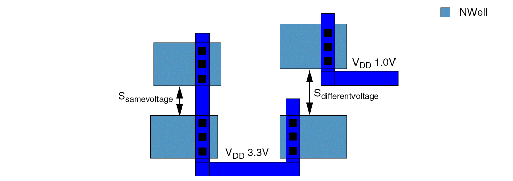
Specifies the minimum spacing between shapes on nets at different voltage levels on the specified layer.
This constraint applies to wells, transistors, and devices. When two geometries, typically two "NWell" shapes, are at different voltages, a larger spacing is required between the two shapes. The larger spacing prevents potential leakage problems through the substrate.
Values
Parameters
Example
The following spacing requirement must be satisfied if a voltage difference exists between two nets on a layer:
- The spacing between two Metal1 shapes must be at least 1.0.
-
The spacing between two Metal2 shapes must be at least equal to the value of the technology parameter
mindiffnetspace1.
spacings(
    ( minDiffNetSpacing "Metal1"
     1.0
 )
 ( minDiffNetSpacing "Metal2"
  techParam("mindiffnetspace1")
 )
) ;spacings
Return to top