Validating Layer Settings for a Package Layout
The layer thicknesses, metal conductivity, dielectric permittivity (Dk) and dielectric loss tangent (Df) in the package layout must match the fab parameters. This ensures that the captured electrical response is correct.
These details are provided in the technology file. You can also view these in the Layer Stack Editor and make changes, if required.
To validate the layer settings for a package design:
-
Choose RF-Module – Setup – Layer Stack Editor to open the Layer Stack Editor.
Validate the details in the form.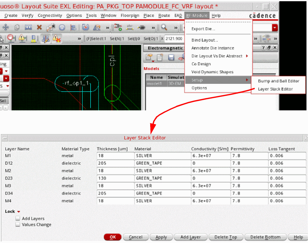
- If the dielectric properties for the metal layers is missing, fill in the data.
- (Optional) Add a dielectric layer on top or bottom of your design layer.
- (Optional) If the layer that exists on top of your design layer is not required, click Delete Top to delete that top layer. Next, click Add Layer to add a new metal or dielectric layer by using the Add Layer form.
Related Topics
Return to top