A
Comparator Macromodel
The comparator macromodel is a parameterized macromodel in the analog circuit design environment. This macromodel uses a simplified equivalent circuit to emulate the DC, AC, and transient nature of a real comparator’s electrical performance.
A macromodel is advantageous because it reduces computation time and space, but it still retains accuracy. The comparator model shown in this topic is a modified model of the Harris level_0 comparator macromodel, which has a simple RC circuit with the clamping stage. This macromodel represents the performance of both the IC comparator and an ideal comparator as accurately as possible.
The comparator macromodel simulates the following effects:
- Input bias current
- Input offset current
- Input offset voltage
- Input resistance
- Input capacitance
- Open loop gain
- Small-signal delay time
- Small-signal rising and falling time
- Overdrive voltage for small-signal transient response test
- Output voltage swing
- Output resistance
Circuit Design
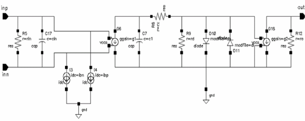
The following figure is a schematic of the comparator macromodel circuit:
Functional Description
There are three stages in the comparator macromodel:
Input Stage
The input stage is built with four components:
The input stage of the comparator macromodel uses a rough linear approximation. The four components model the input current versus voltage variation around the active region. However, the input stage does not model the saturation and cutoff effects of the input currents and terminal resistances.
Gain and Delay Stage
The gain and delay stage is constructed with a voltage-controlled current source and a single RC time constant circuit.
G1, C1, Cx, and Rd create a single pole roll-off amplifier circuit. Rx, Rd, and G1 model small signal gain.
The clamping voltages of the two diodes Dh and Dl are set to the value of the positive and negative output voltage swing. These diodes are built to be referenced directly to ground. If the negative output voltage swing VOL is defined as zero like the default value, an independent voltage source of value VOH/2 is inserted between the diodes and ground. This allows the output voltages to have symmetric limiting characteristics.
Output Stage
G2 and RO build the output stage, which forms a gain of one buffer. G2 is put there to isolate the gain stage and the outside load to reduce the unwanted influence of the load to the modeling of delay time.
Comparator Macromodel Netlist
The following shows a netlist of the comparator macromodel:
# comparator 0.s
# Description:  Small signal model of input stage, no
#               Io limits or power supply effects, simple
#               resistive input stage, small large signal
#               delay, constant Rout and no current limit
#
# Format:
#
# USE  comparator name ibias vos ios rin cin voh vol vis trs tds gol ro
#     &1 &2 &3 &4 &5 &6 &7 &8 &9 &10 &11 &12 &13
#
# Default values of the parameters:
#
# &1   model name                                 name = &1
# &2   Input bias current                         ibias = 200n
# &3   Input offset voltage                       vos = 0
# &4   Input offset current                       ios = 10n
# &5   Input resistance                           rin = 1meg
# &6   Input capacitance                          cin = 1p
# &7   Positive output voltage swing              voh = 5
# &8   Negative output voltage swing              vol = 0
# &9   Overdrive voltage for delay time test      vis = 2m
# &10  Small signal rising and falling time test  trs = 20n
# &11  Small signal delay time                    tds = 50n
# &12  Open loop game                             gol = 100k
# &13  Output resistance                          ro = 200
#
.subckt &1 10 20 30
#
# Input stage
#
RIN   10  20   (&5)
CIN   10  20   (&6)
IBP   10  0    (&2) +(&4)/2
IBN   20  0    (&2) -(&4)/2
#
# Gain Stage
#
G1  0   2   poly    1  10  20 =-(&3)*(&12)  1E5=(&12)/1E5
C1  2   0   ((&11-&10/2)/log(2))/(1E5/&
             (&12*(&9)*(&10)/(&7-(&8))/((&11-&10/2)/log(2))-1))
RX  2   3   1E5/(&12*(&9)*&10/(&7-(&8))/((&11-&10/2)/log(2))-1)
#
If &7*(&8)<>0 then
  RD   3 0   1E5
  DH   3 0   DH
  DL   0 3   DL
 .MODEL DH D  IS = 0.3*(&12)/1E33  N = &7/VT/LOG(1E28)
 .MODEL DL D  IS = 0.3*(&12)/1E33  N = -(&8)/VT/LOG(1E28)
else
  RD   3 8    1E5
  DH   3 8    DM
  DL   8 3    DM
  VM   8 0    (&7+(&8))/2
 .MODEL DM D  IS=0.3*(&12)/1E33  N=(&7+&(&8))/2/VT/LOG(1E28)
endif
#
#   Output Stage
#
RO  0 30   (&13)
G2  0 30   poly 1 3 0  0 =1/(&13+0.1)
.ends &1
Example
Return to top