Bulk Area Connectivity Extraction
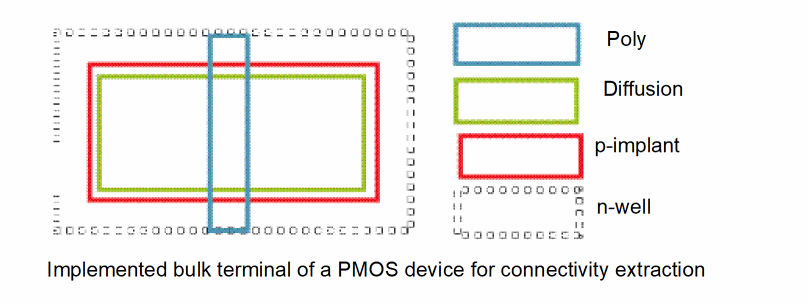
The bulk area of a transistor can be defined using a physical and extractable pin figure or using a shapeless terminal. If the bulk is implemented using a physical shape, the corresponding pin figures define the bulk area and the extractor uses the corresponding layer(s) to determine the top-level connections. If the bulk is a shapeless terminal, the bulk area of the device is usually the active layer that lies under its gate, between the source and the drain. The following figure displays the bulk area of a PMOS device, which is a physical shape on the Nwell layer.
The following figure displays the bulk area of an NMOS device for a shapeless bulk terminal.
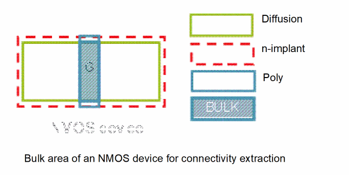
When the bulk terminal is shapeless, the corresponding bulk area needs to be derived by the extractor. For more information, see Identifying the Bulk Area.
Bulk area connectivity extraction means that the extractor recognizes the bulk area as an extractable layer even when the terminal is shapeless.
The bulk area is considered as “fully” extractable because the bulk is recognized by the extractor even if it does not have a physical shape drawn. When an instance terminal without an extractable layer has its pinFig-less layer defined as "substrate", the PR boundary in the master is used to define the geometry of the bulk area.
For the extractor to derive connectivity information from the bulk area, here are the tasks that need to be performed:
- Bulk Area Connectivity Extraction - Identifying the Substrate Area
- Bulk Area Connectivity Extraction - Isolating the Substrate and Well Layers
- Bulk Area Connectivity Extraction - Identify the Bulk Area
- Bulk Area Connectivity Extraction - Identify the Substrate and Well Tap Vias
Return to top