2
Active Components
All components listed in the Actives category require a defined model card. Each element maps to a specific Spectre primitive with respect to its instance parameters.
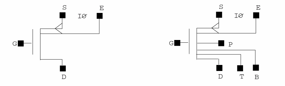
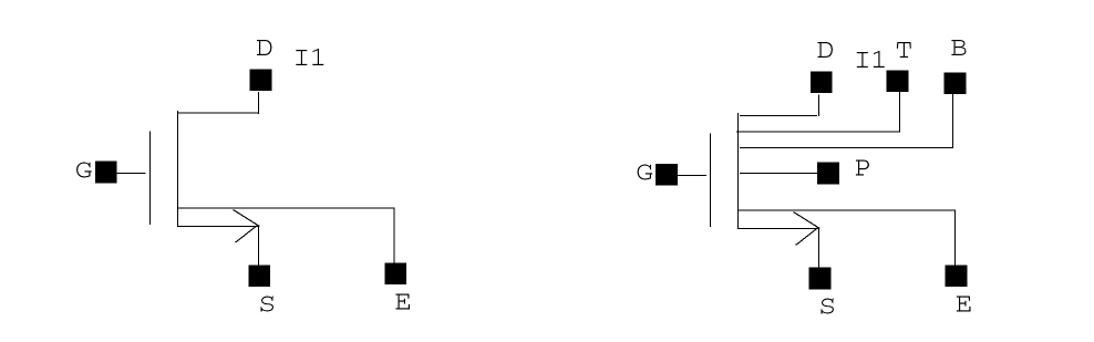
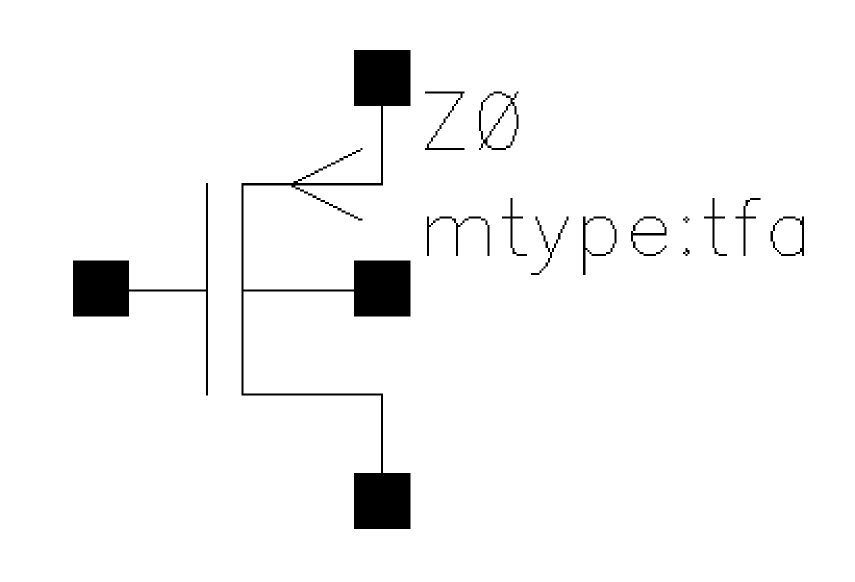
Symbol: ibis_buffer
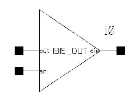
The IBIS buffer model is based on the IBIS (I/O Buffer Information Specification) standard, version 3.2. The package and board models are not included in the buffer, they have to be added as separate subcircuits.
The ibis_buffer component is a p-cell that can have different pin combinations based on the selected buffer type. The supported buffer types are:
- input
- output
- io
- tristate
- opendrain and opensink
- ioopendrain and ioopensink
- opensource
- ioopensource
- terminator
- inputecl
- outputecl
- ioecl
- tristateecl
The following table lists the different pin combinations based on the buffer type. The presence of a pin is denoted by Y, absence of a pin is denoted by N, and optional pin is denoted by O.
| Buffer Type | die/pad pin | input | output | enable | ground | power | ground clamp | power clamp | inverted die/pad pin |
|---|---|---|---|---|---|---|---|---|---|
For each buffer type there can be four variants, internal_power, external_power,
differential _input, and diff_inp_and_ext_pwr. Therefore, ibis_buffer can have 44 variants as shown in the following table.
| Buffer Type | Variant | die/pad | in | out | en | gnd | pwr | gnd_c | pwr_c | inv_die | |
|---|---|---|---|---|---|---|---|---|---|---|---|
Based on the model you have selected, you can create two types of ibis_buffer:
-
with an external model card
This is the default option. If you specify the model name the netlist is as follows:b1 (1 2 3) "Model name" <other instance parameters>
For example, the netlist of an ibis_buffer with buffer type =tristate, buffer variant =internal_power, model name =SN74_OUT_33_Typ_27degC, polarity =inv, differential threshold =1.2V, delay time =1ms, delay schedule =yes, different element delays =1p,2p,5p, and2p, is as follows:I65 (net013 net011 net012) SN74_OUT_33_Typ_27degC polarity=inv \ vdiff=1.2 delay=1m delay_schedule=[1p 2p 5p 2p]
-
with an IBIS file
If you specify an IBIS buffer file, then three additional parameters are displayed. In this case the netlist is as follows:b1 (1 2 3) ibis_buffer file="IBIS file name" model="IBIS model name" corner="IBIS model corner" <other instance parameters>
For example, the netlist with the additional parameters IBIS filename =~/main.scs, IBIS modelname =IBIS_Model, corner =typicalis as follows:I65 (net013 net011 net012) ibis_buffer file="~/main.scs" \ model="IBIS_Model" corner=typical polarity=inv vdiff=1.2 delay=1m \ delay_schedule=[1p 2p 5p 2p]
Command-line help
CDF Parameters
| CDF Parameter Label | CDF Parameter | spectre | auCdl | auLvs | hspiceD | UltraSim |
|---|---|---|---|---|---|---|
Syntax/Synopsis
Name ( die [inp] [out] [en] [gnd] [pwr] [gnd_c] [pwr_c] [inv_die] ) ModelName
<parameter=value> ...
Name ( die [inp] [out] [en] [gnd] [pwr] [gnd_c] [pwr_c] [inv_die] )
ibis_buffer <parameter=value> ...
Example
I65 (net013 net011 net012) SN74_OUT_33_Typ_27degC polarity=inv \
vdiff=1.2 delay=1m delay_schedule=[1p 2p 5p 2p]
b1 (1 2 3) ibis_buffer file="IBIS file name" model="IBIS model name" corner="IBIS model corner" <other instance parameters>
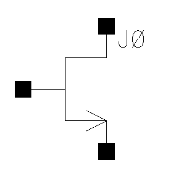
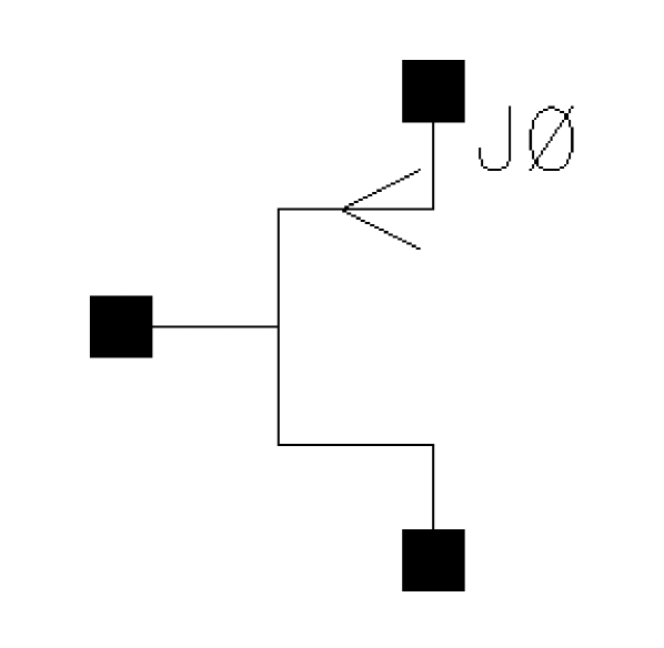
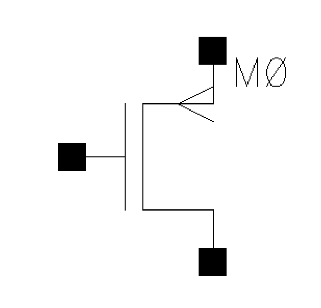
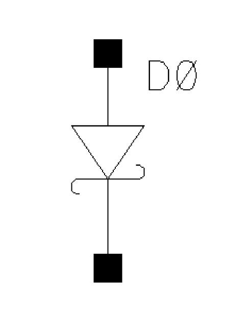
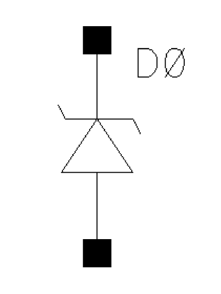
Symbol: diode
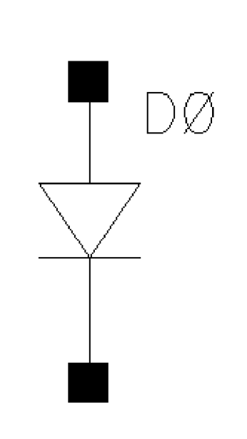
The junction diode model includes nonlinear junction capacitance and reverse breakdown.
Command-line help
Component Parameters
| CDF Parameter Label | CDF Parameter | spectre | auCdl | auLvs | hspiceD | UltraSim |
|---|---|---|---|---|---|---|
Syntax/Synopsis
Name ( a c ) ModelName <parameter=value> ...
In the forward operation the voltage on the anode (‘a’) is more positive than the voltage on the cathode (‘c’).
Model Synopsis
model ModelName diode <parameter=value> ...
Example
d0 (dp dn) pdiode l=3e-4 w=2.5e-4 area=1
model pdiode diode is=1.8e-5 rs=1.43 n=1.22 nz=2.31 gleak=6.2e-5
rsw=10 isw=6.1e-10 ibv=0.95e-3 tgs=2 ik=1.2e7 fc=0.5 cj=1.43e-3
pb=0.967 mj=0.337 cjsw=2.76e-9 vjsw=0.94 jmax=1e20
Additional Information
This device is supported within the altergroups.
Symbol: nbsim
N-type BSIM Field Effect Transistor
nbsim is an n-channel BSIM model.
Command-line help
For related information on MOS, use any of the following help commands:
CDF Parameters
| CDF Parameter Label | CDF Parameter | spectre | auCdl | auLvs | hspiceD | UltraSim |
|---|---|---|---|---|---|---|
Syntax/Synopsis
Name ( d g s b ) ModelName <parameter=value> ...
model ModelName bsim1 <parameter=value> ...
Example
m1 (1 2 0 0) nchmod l=5u w=10u as=40u ad=40u pd=28u ps=28u m=1
model nchmod bsim1 vfb0=-0.5 lvfb=0.5 wvfb=0.3 phi0=0.8 eta0=0.056 k1=0.5 muz=454 eg=0.99 gap1=5.5e-04 trs=1e-3 trd=1e-3 xpart=0.5 rs=10 rd=10
Additional Information
This device is supported within the altergroups.
Symbol: nbsim4
N-type BSIM MOS transistor (4 terminals)
BSIM4 is the version-4.21 of the bsim model. BSIM4 transistors require you to use a model statement.
Command-line help
For related information on MOS, use any of the following help commands:
CDF Parameters
The CDF parameters for nbsim4 are the same as the CDF parameters for nbsim.
Syntax/Synopsis
Name ( d g s b ) ModelName <parameter=value> ...
model ModelName bsim4 <parameter=value> ...
Example
m4 (0 2 1 1) pchmod w=2u l=0.8u as=250p ad=250p pd=168p ps=168p m=1
model pchmod bsim4 type=p mobmod=0 capmod=2 version=4.21 toxe=3e-9
cdsc=2.58e-4 cdscb=0 cdscd=6.1e-8 cit=0 nfactor=1.1 xj=9e-8
vfb=0.76vsat=9.2e4 at=3.3e4 a0=1.1 ags=1.0e-20 a1=0 ngate=9e19
vth0=-0.42a1=0 a2=1 delta=0.014 pvag=1e-20 pclm=6.28e-4 pdits=0.2
pditsl=2.3e6pditsd=0.23 fprout=0.2 pdiblcb=3.4e-8 pdiblc1=0.81
drout=0.56pdiblc2=9.84e-6 pscbe1=8.14e8 pscbe2=9.58e-07 lint=5e-9
wint=5e-9dmcg=5e-6 dmci=5e-6 dmdg=5e-6 dmcgt=6e-7 dwj=4.5e-8
rsh=6cgso=7.43e-10 cgdo=7.43e-10 cgbo=2.56e-11 cgsl=1e-14
cgdl=1e-14ckappas=0.5 ckappad=0.5 noff=0.9 voffcv=0.02 acde=1 moin=15
xpart=0kt1l=0 kt2=2.2e-2 lpe0=5.75e-8 lpeb=2.3e-10 dvt0=2.89
dvt1=0.53dvt2=-3.2e-2 dvt0w=0 dvt1w=0 dvt2w=0 dvtp0=7.32e-7
dvtp1=0.12dsub=0.058 eta0=0.001 u0=4.19e-2 ua=8.7e-16 ub=3.06e-18
k1=0.33uc=4.6e-13 ute=-1.5 ua1=4.31e-9 ub1=7.61e-18 uc1=-5.6e-11
k2=-1.87e-2rdsw=369.4 rdw=184.7 rsw=184.7 prwg=3.22e-8 prwb=6.8e-11
wr=1rdswmin=0 rdwmin=0 rswmin=0 prt=0 b0=-1e-20 k3=80 k3b=0
w0=2.5e-6b1=0 keta=-0.047 alpha0=7.4e-2 alpha1=0.005 beta0=30
Additional Information
This device is supported within the altergroups.
Symbol: njfet
N-type Junction Field Effect Transistor
The JFET model is derived from the FET model of Shichman and Hodges. JFETs require you to use a model statement.
Command-line help
CDF Parameters
| CDF Parameter Label | CDF Parameter | spectre | auCdl | auLvs | hspiceD | UltraSim |
|---|---|---|---|---|---|---|
Syntax/Synopsis
Name ( d g s [b] ) ModelName <parameter=value> ...
You do not have to specify the back gate terminal when you use the four-terminal model. If left unspecified, the substrate is connected to ground.
model ModelName jfet <parameter=value> ...
Example
jf1 (net1 net2 0) jmod area=1
model jmod jfet beta=9e-5 lambda=0 type=n vt0=-18.7 rd=10 rs=10 cgs=1.3e-13 pb=0.65
Additional Information
This device is supported within the altergroups.
Symbol: nmes
The GaAs MESFET model was derived from the model by H. Statz and others at Raytheon. This model is completely symmetric and is modified slightly to make it charge conserving. GaAs MESFET instances require that you use a model statement.
Command-line help
CDF Parameters
| CDF Parameter Label | CDF Parameter | spectre | auCdl | auLvs | hspiceD | UltraSim |
|---|---|---|---|---|---|---|
Syntax/Synopsis
Name ( d g s ) ModelName <parameter=value> ...
model ModelName gaas <parameter=value> ...
Example
m1 (1 2 0) nmes area=1 m=2
model nmes gaas type=n vto=-2 beta=0.06 lambda=0 b=0.25 rs=3.65 alpha=1.9 rd=1.98 is=1.1e-9 n=1.28 fc=0.5 cgs=0.365e-12
Additional Information
This device is supported within the altergroups.
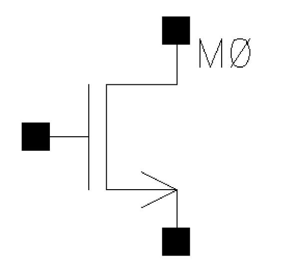
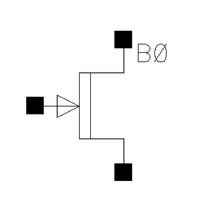
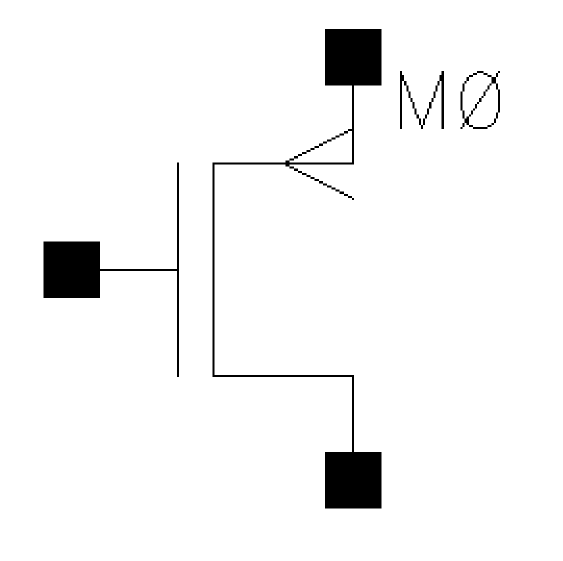
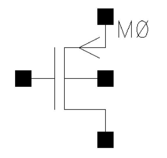
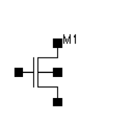
Symbol: nmos
N-type Generic MOS Transistor (3 terminals)
Command-line help
For related information on MOS, use any of the following help commands:
CDF Parameters
| CDF Parameter Label | CDF Parameter | spectre | auCdl | auLvs | hspiceD | UltraSim |
|---|---|---|---|---|---|---|
Example
M0 (net3 net1 net2) nmos
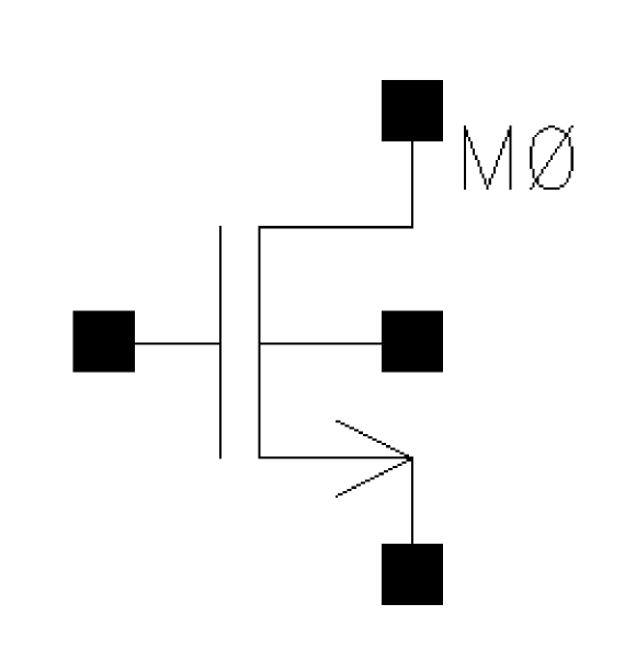
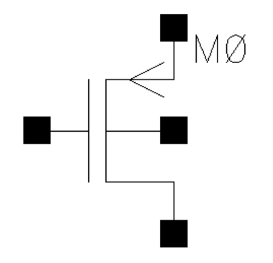
Symbol: nmos4
N-type Generic MOS Transistor (4 terminals)
Command-line help
For related information on MOS, use any of the following help commands:
CDF Parameters
The CDF parameters for nmos4 are the same as the CDF parameters for nmos.
Example
M0 (net1 net3 net4 net2) nmos4
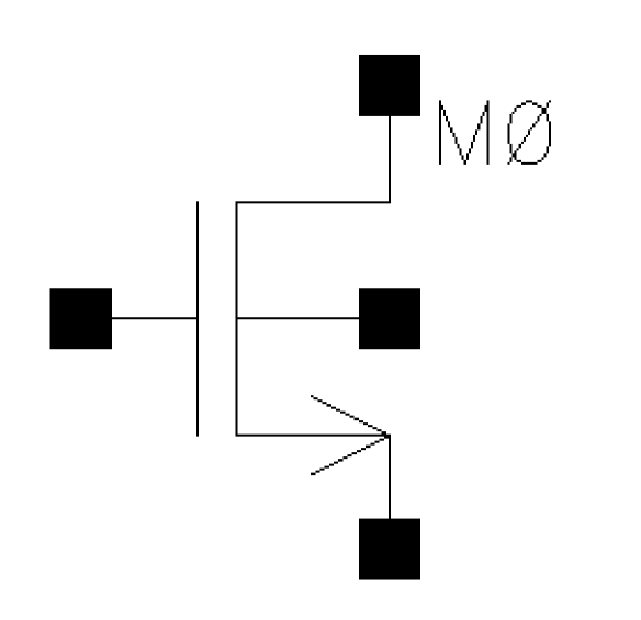
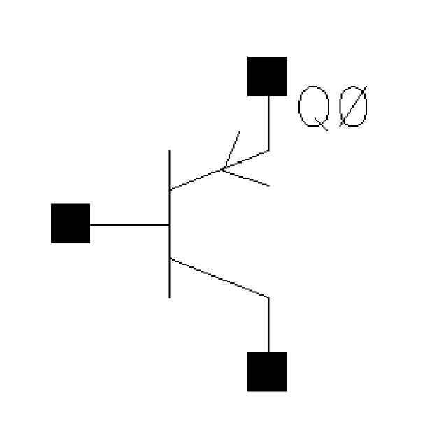
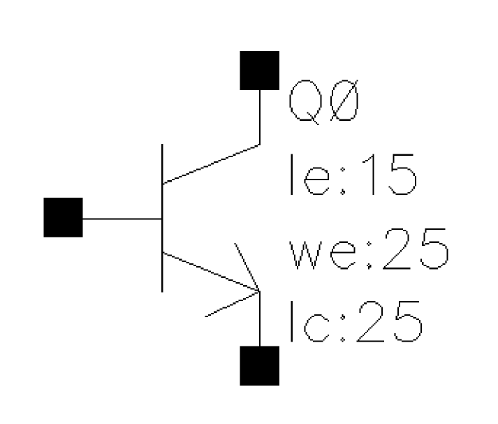
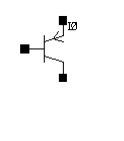
Symbol: npn
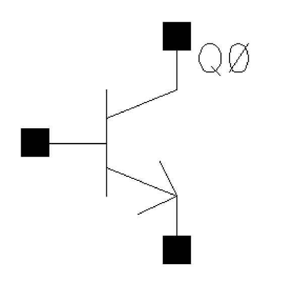
Generic Bipolar Transistor (NPN)
Command-line help
CDF Parameters
| CDF Parameter Label | CDF Parameter | spectre | auCdl | auLvs | hspiceD | UltraSim |
|---|---|---|---|---|---|---|
Syntax/Synopsis
Name ( c b e [s] ) ModelName <parameter=value> ...
You do not have to specify the substrate terminal. If you do not specify it, the substrate is connected to ground.
model ModelName bjt <parameter=value> ...
Example
q1 (vcc net3 minus) npn_mod region=fwd area=1 m=1
Following is a sample model statement:
model npn_mod bjt type=npn is=10e-13 bf=200 va=58.8 ikf=5.63e-3 rb=700 rbm=86 re=3.2 cje=0.352e-12 pe=0.76 me=0.34 tf=249e-12 cjc=0.34e-12 pc=0.55
Additional Information
This device is supported within the altergroups.
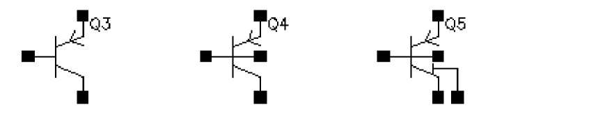
Symbol: ntft
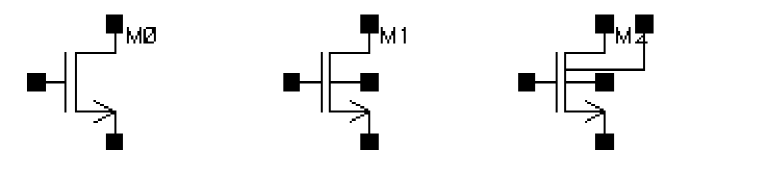
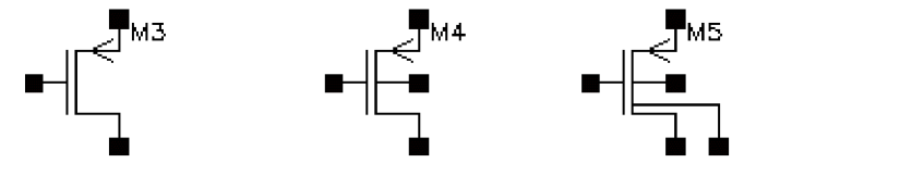
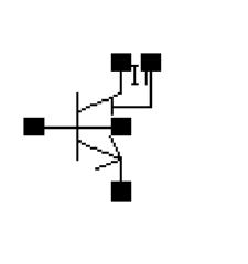
ntft is an n-type polysilicon tft. It can have a maximum of five terminals with drain, gate and source being mandatory terminals and substrate and thermal being optional.
The diagrams show the terminal with none, one or two optional nodes selected.
Command-line help
CDF Parameters
| CDF Parameter Label | CDF Parameter | spectre | spectreS | cdsSpice | auCdl | auLvs | hspiceS | hspiceD | UltraSim |
|---|---|---|---|---|---|---|---|---|---|
Syntax/Synopsis
Name ( d g s [b] [t] ) ModelName <parameter=value> ...
model ModelName psitft <parameter=value> ...
Sample Instance Statement
m4 (0 2 1 1 3) nch w=2u l=0.8u
Sample Model Statement
model nch psitft type=n
Additional Information
This device is supported within the altergroups.
Symbol: pbsim
P-type BSIM MOS Transistor (3 terminals)
pbsim is a p-channel BSIM model.
Command-line help
For related information on MOS, use any of the following help commands:
CDF Parameters
| CDF Parameter Label | CDF Parameter | spectre | auCdl | auLvs | hspiceD | UltraSim |
|---|---|---|---|---|---|---|
Syntax/Synopsis
Name ( d g s b ) ModelName <parameter=value> ...
Following is the model synopsis:
model ModelName bsim1 <parameter=value> ...
Example
m1 (1 2 0 0) nchmod l=5u w=10u as=40u ad=40u pd=28u ps=28u m=1
Following is the sample model statement:
model nchmod bsim1 vfb0=-0.5 lvfb=0.5 wvfb=0.3 phi0=0.8 eta0=0.056 k1=0.5
muz=454 eg=0.99 gap1=5.5e-04 trs=1e-3 trd=1e-3 xpart=0.5 rs=10 rd=10
Additional Information
This device is supported within the altergroups.
Symbol: pbsim4
P-type BSIM MOS transistor (4 terminals)
pbsim is a p-channel BSIM model.
Command-line help
For related information on MOS, use any of the following help commands:
CDF Parameters
The CDF parameters for pbsim4 are the same as the CDF parameters for pbsim.
Syntax/Synopsis
Name ( d g s b ) ModelName <parameter=value> ...
Following is the model synopsis:
model ModelName bsim1 <parameter=value> ...
Example
m1 (1 2 0 0) nchmod l=5u w=10u as=40u ad=40u pd=28u ps=28u m=1
Following is the sample model statement:
model nchmod bsim1 vfb0=-0.5 lvfb=0.5 wvfb=0.3 phi0=0.8 eta0=0.056 k1=0.5
muz=454 eg=0.99 gap1=5.5e-04 trs=1e-3 trd=1e-3 xpart=0.5 rs=10 rd=10
Additional Information
This device is supported within the altergroups.
Symbol: pjfet
P-type Junction Field Effect Transistor
The JFET model is derived from the FET model of Shichman and Hodges. JFETs require you to use a model statement.
Command-line help
CDF Parameters
| CDF Parameter Label | CDF Parameter | spectre | auCdl | auLvs | hspiceD | UltraSim |
|---|---|---|---|---|---|---|
Syntax/Synopsis
Name ( d g s [b] ) ModelName <parameter=value> ...
You do not have to specify the back gate terminal when you use the four-terminal model. If left unspecified, the substrate is connected to ground.
model ModelName jfet <parameter=value> ...
Example
jf1 (net1 net2 0) jmod area=1
Following is a sample model statement:
model jmod jfet beta=9e-5 lambda=0 type=n vt0=-18.7 rd=10 rs=10 cgs=1.3e-13 pb=0.65
Additional Information
This device is supported within the altergroups.
Symbol: psoip
psoip is a p-type BSIM SOI model
Command-line help
CDF Parameters
| CDF Parameter Label | CDF Parameter | spectre | auCdl | auLvs | hspiceD | UltraSim |
|---|---|---|---|---|---|---|
Syntax/Synopsis
Name ( d g s e [p] [b] [t] ) ModelName <parameter=value> ...
Following is the model synopsis:
model ModelName bsimsoi <parameter=value> ...
Example
I7 (0 net9 vdd! vdd!) bsimsoi w=1u 1=1u
Following is the sample model statement:
model psoip_model bsimsoi type = p beta0 = 0 dvt = -0.032 delta = 0.01 k1 = 0.6 xbjt = 1 kt1 = -0.11 ndif = -1 noif = 1 vsdfb = 0 vevb = 0.075 dvt1 = 0.53
Additional Information
In psoip, there are four optional parameters in the CDF properties of the p-cell:
There can be a number of permutaions and combinations for these pins, however, only following seven permutaions are supported:
Symbol: nsoip
nsoip is a n-type BSIM SOI model
Command-line help
CDF Parameters
| CDF Parameter Label | CDF Parameter | spectre | auCdl | auLvs | hspiceD | UltraSim |
|---|---|---|---|---|---|---|
Syntax/Synopsis
Name ( d g s e [p] [b] [t] ) ModelName <parameter=value> ...
Following is the model synopsis:
model ModelName bsimsoi <parameter=value> ...
Example
I6 (vdd! net9 0 0 ) bsimsoi w=1u 1=1u
Following is the sample model statement:
model nsoip_model bsimsoi type = n beta0 = 0 dvt = -0.032 delta = 0.01 k1 = 0.6 xbjt = 1 kt1 = -0.11 ndif = -1 noif = 1 vsdfb = 0 vevb = 0.075 dvt1 = 0.53
Additional Information
In nsoip, there are four optional parameters in the CDF properties of the n-cell:
There can be a number of permutaions and combinations for these pins, however, only following seven permutaions are supported:
if Tnodeout=0 or not given (default is 0)
Symbol: pmos
P-type Generic MOS Transistor (3 terminals)
Command-line help
For related information on MOS, use any of the following help commands:
CDF Parameters
| CDF Parameter Label | CDF Parameter | spectre | auCdl | auLvs | hspiceD | UltraSim |
|---|---|---|---|---|---|---|
Symbol: pmos4
P-type Generic MOS Transistor (4 terminals)
Command-line help
For related information on MOS, use any of the following help commands:
CDF Parameters
The CDF parameters for pmos4 are the same as the CDF parameters for pmos.
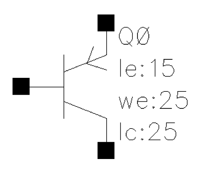
Symbol: pnp
Generic Bipolar Transistor (PNP)
Command-line help
CDF Parameters
| CDF Parameter Label | CDF Parameter | spectre | auCdl | auLvs | hspiceD | UltraSim |
|---|---|---|---|---|---|---|
Syntax/Synopsis
Name ( c b e [s] ) ModelName <parameter=value> ...
You do not have to specify the substrate terminal. If you do not specify it, the substrate is connected to ground.
Following is the model synopsis:
model ModelName bjt <parameter=value> ...
Example
q1 (vcc net3 minus) npn_mod region=fwd area=1 m=1
Following is a sample model statement:
model npn_mod bjt type=npn is=10e-13 bf=200 va=58.8 ikf=5.63e-3 rb=700
rbm=86 re=3.2 cje=0.352e-12 pe=0.76 me=0.34 tf=249e-12 cjc=0.34e-12
pc=0.55
Additional Information
This device is supported within the altergroups.
Symbol: ptft
ptft is a p-type polysilicon tft. It can have a maximum of five terminals with drain, gate and source being mandatory terminals and substrate and thermal being optional.
The diagrams show the terminal with none, one or two optional nodes selected.
Command-line help
CDF Parameters
| CDF Parameter Label | CDF Parameter | spectre | spectreS | cdsSpice | auCdl | auLvs | hspiceS | hspiceD | UltraSim |
|---|---|---|---|---|---|---|---|---|---|
Syntax/Synopsis
Name ( d g s [b] [t] ) ModelName <parameter=value> ...
model ModelName psitft <parameter=value> ...
Sample Instance Statement
m4 (0 2 1 1 3) nch w=2u l=0.8u
Sample Model Statement
model nch psitft type=p
Additional Information
This device is supported within the altergroups.
Symbol: psoi
CDF Parameters
| CDF Parameter Label | CDF Parameter | spectre | auCdl | auLvs | hspiceD | UltraSim |
|---|---|---|---|---|---|---|
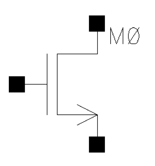
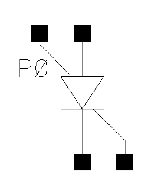
Symbol: schottky
A special type of diode that has a low forward-voltage drop leading to greater system efficiency.
Command-line help
CDF Parameters
| CDF Parameter Label | CDF Parameter | spectre | auCdl | auLvs | hspiceD | UltraSim |
|---|---|---|---|---|---|---|
Example
D0 (net1 net2) schottky
Symbol: usernpn
User Specific NPN Bipolar Transistor (3 terminals)
Command-line help
CDF Parameters
| CDF Parameter Label | CDF Parameter | spectre | auCdl | auLvs | hspiceD | UltraSim |
|---|---|---|---|---|---|---|
Syntax/Synopsis
Name ( c b e [s] ) ModelName <parameter=value> ...
You do not have to specify the substrate terminal. If you do not specify it, the substrate is connected to ground.
model ModelName bjt <parameter=value> ...
Example
q1 (vcc net3 minus) npn_mod region=fwd area=1 m=1
model npn_mod bjt type=npn is=10e-13 bf=200 va=58.8 ikf=5.63e-3 rb=700 rbm=86
re=3.2 cje=0.352e-12 pe=0.76 me=0.34 tf=249e-12 cjc=0.34e-12 pc=0.55
Additional Information
This device is supported within the altergroups.
Symbol: userpnp
User Specific PNP Bipolar Transistor (3 terminals)
Command-line help
CDF Parameters
| CDF Parameter Label | CDF Parameter | spectre | auCdl | auLvs | hspiceD | UltraSim |
|---|---|---|---|---|---|---|
Symbol: vnpn
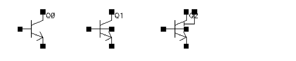
Variable Bipolar Transistor (VNPN)
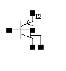
vnpn is a variable terminal n-type bjt. It can have a maximum of five terminals with collector, emitter and base being mandatory terminals and substrate and thermal being optional.
The diagrams show the terminal with none, one or two optional nodes selected.
Command-line help
CDF Parameters
| CDF Parameter Label | CDF Parameter | spectre | spectreS | cdsSpice | auCdl | auLvs | hspiceS | hspiceD | UltraSim |
|---|---|---|---|---|---|---|---|---|---|
Syntax/Synopsis
Name ( c b e [s] ) ModelName <parameter=value> ...
You do not have to specify the substrate terminal. If you do not specify it, the substrate is connected to ground.
model ModelName bjt <parameter=value> ...
Example
q1 (vcc net3 minus) npn_mod region=fwd area=1 m=1
Following is a sample model statement:
model npn_mod bjt type=npn is=10e-13 bf=200 va=58.8 ikf=5.63e-3 rb=700 rbm=86 re=3.2 cje=0.352e-12 pe=0.76 me=0.34 tf=249e-12 cjc=0.34e-12 pc=0.55
Additional Information
This device is supported within the altergroups.
Symbol: vpnp
Variable Bipolar Transistor (VPNP)
vpnp is a variable terminal p-type bjt. It can have a maximum of five terminals with collector, emitter and base being mandatory terminals and substrate and thermal being optional.
The diagrams show the terminal with none, one or two optional nodes selected.
Command-line help
CDF Parameters
| CDF Parameter Label | CDF Parameter | spectre | spectreS | cdsSpice | auCdl | auLvs | hspiceS | hspiceD | UltraSim |
|---|---|---|---|---|---|---|---|---|---|
Syntax/Synopsis
Name ( c b e [s] ) ModelName <parameter=value> ...
You do not have to specify the substrate terminal. If you do not specify it, the substrate is connected to ground.
Following is the model synopsis:
model ModelName bjt <parameter=value> ...
Example
q1 (vcc net3 minus) npn_mod region=fwd area=1 m=1
Following is a sample model statement:
model npn_mod bjt type=npn is=10e-13 bf=200 va=58.8 ikf=5.63e-3 rb=700
rbm=86 re=3.2 cje=0.352e-12 pe=0.76 me=0.34 tf=249e-12 cjc=0.34e-12
pc=0.55
Additional Information
This device is supported within the altergroups.
Symbol: zener
It has p-n junction in reverse bias to use the zener effect to maintain a constant voltage.
Command-line help
CDF Parameters
| CDF Parameter Label | CDF Parameter | spectre | auCdl | auLvs | hspiceD | UltraSim |
|---|---|---|---|---|---|---|
auCdl and auLvs Components
The following components are supported only by auCdl or auLvs.
Symbol: nsoi
CDF Parameters
| CDF Parameter Label | CDF Parameter | spectre | auCdl | auLvs | hspiceD | UltraSim |
|---|---|---|---|---|---|---|
Symbol: scr
Silicon Controlled Rectifier
scr is a conventional rectifier controlled by a gate signal. Although the main circuit is a rectifier, the application of a forward voltage is not enough for conduction. Therefore, a gate signal controls the rectifier conduction.
CDF Parameters
| CDF Parameter Label | CDF Parameter | spectre | auCdl | auLvs | hspiceD | UltraSim |
|---|---|---|---|---|---|---|
Example
P231 32 5 21 8 7 PSCR
PN01 25 14 18 2 PMOD IC=-.8 .8 -15
Symbol: bjt504tnpn
Compact Bipolar-Transistor Model
The bjt504 model provides a detailed description of a vertical integrated NPN transistor.
Command-line help
CDF Parameters
| CDF Parameter Label | CDF Parameter | spectre | spectreS | cdsSpice | auCdl | auLvs | hspiceS | hspiceD | UltraSim |
|---|---|---|---|---|---|---|---|---|---|
Syntax/Synopsis
Name ( c b e s ) ModelName <parameter=value> ...
Symbol: bjt504tpnp
Compact Bipolar-Transistor Model
The bjt504 model provides a detailed description of a vertical integrated PNP transistor.
Command-line help
CDF Parameters
| CDF Parameter Label | CDF Parameter | spectre | spectreS | cdsSpice | auCdl | auLvs | hspiceS | hspiceD | UltraSim |
|---|---|---|---|---|---|---|---|---|---|
Syntax/Synopsis
Name ( c b e s ) ModelName <parameter=value> ...
Symbol: bsim4
This component is a simple BSIM MOS transistor.
Command-line help
CDF Parameters
| CDF Parameter Label | CDF Parameter | spectre | spectreS | cdsSpice | auCdl | auLvs | hspiceS | hspiceD | UltraSim |
|---|---|---|---|---|---|---|---|---|---|
Syntax/Synopsis
Name ( d g s b ) ModelName <parameter=value> ...
Symbol: vbic
This component is a bipolar transistor.
Command-line help
CDF Parameters
| CDF Parameter Label | CDF Parameter | spectre | spectreS | cdsSpice | auCdl | auLvs | hspiceS | hspiceD | UltraSim |
|---|---|---|---|---|---|---|---|---|---|
Syntax/Synopsis
Name ( c b e [s] [dt] [tl] ) ModelName <parameter=value> ...
Return to top