E
Application Techniques
Bipolar Processing
The Diva verification LPE program is technology independent. Most of the examples used in this manual are MOS because this is the easiest technology to understand and apply. This section introduces you to bipolar technologies which are more complex and require a slightly different application technique. The version of bipolar used in the example, though it might not exist, provides an easy-to-understand illustration that can be extrapolated to real technologies.
General Technique
The first step in the encoding of a bipolar technology is to determine all the devices you need to recognize. Within a single bipolar process, using a single set of mask or design layers, many different types of devices can be formed (for example, transistors, different kinds of diodes, resistors, and capacitors) as well as special contacts and ties. If you consider only a subset of these devices, the extraction fails because the layout includes devices not yet handled. To recognize those extra devices might require a complete redefinition of the original device recognition. For each device in the process, you need a “plan” view illustrating the topology relationships and a section showing the vertical layer relationships and current paths.
Minor topological variations change the type of device being represented. A Pbase region is performed as a single diode in one case, but the addition of an Ndiffusion (Ndiff) transforms it into a transistor. A contact in the Pbase is just a base contact until it overlaps into the Ntub, where it becomes a Schottky diode.
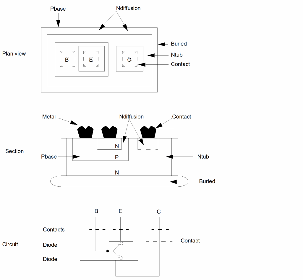
The major obstacle in bipolar recognition is the misinterpretation of which topological (layer/mask) relationships perform what functions. The first example shows the plan view of an npn transistor which is commonly misinterpreted. It appears obvious which is the emitter, base, and collector of this device, but in fact it is not.
The shapes in the diagram labeled E, B, and C are not terminals but contacts to interconnect layers that lead to the device terminals. The npn transistor is really two N-P diodes back to back. The terminal labeled “base” is a contact to the Pbase region which forms the P region of the N-P-N configuration between the two diodes. It also acts as the conductor to the “outside world” from that device region. The terminal labeled “emitter” is in fact a contact to the Ndiff, which acts as a conductor down to the P region where the N-P interface forms one of the diodes.
The “collector” is a contact to another Ndiff, which, in turn, acts as a conductor and a contact to the Ntub of the device which also acts as a conductor to the interface between itself and the P region, forming the other P-N diode. The critical parts for recognizing the device are the N-P interfaces. The remainder of the structure just serves to interconnect those parts. This can be best seen from the sectional view, in which the diodes and contacts are highlighted, and from the extracted circuit diagram.
Device Recognition Shape Determination
Diva’s LPE program requires a recognition polygon to represent the device. Since it is created vertically, there are three possible shapes that can be used. The Ntub seems to be the obvious choice until you consider that more than one transistor can be created within a single tub. Such devices have a common collector net, which is an example of how the tub needs to be considered as an interconnect layer to the collector rather than as the device itself.
If you choose the Pbase region as the device recognition polygon, the existence of multiple Ndiff regions within the base region gives rise to a multiple emitter device. This can in fact be what you want, but remember that each device recognized must be available in the system device library for it to be placed in the extracted cellview. The Ndiff inside the Pbase is the simplest polygon to use for device recognition. Each individual shape of diffusion creates a single three-terminal transistor.
If two or more diffusions are within the same P region, that region acts as an interconnect, giving them a common base region, and the tub acts as a common collector region. There is no difference between a multi-emitter device and multiple three-terminal devices with connected bases and connected collectors.
Device Recognition Process
After you have identified the functional parts of all the devices, encode the devices. The simplest approach here is one of elimination. Again, this is best illustrated by example.
Consider a Pbase region used in the definition of a number of different devices such as a diode, transistor, resistor, and so forth. Choose one of these having a unique set of layers. Maybe the only device in which Ndiff sits inside the Pbase is a transistor. Create the commands to recognize that device, and then “and-not” that specific Pbase with the whole to produce a subset of the layer. The transistor is eliminated and can be forgotten.
Now start afresh with the remaining devices. Most device topologies are unique in some manner or other. One by one, choose whatever is unique about the device and use that fact to recognize it, or a part of it. You can then eliminate the recognized features from the remainder. The word “device” in this case includes all structures, including contacts.
Some devices can appear to have no unique features. The terminals of a base resistor look exactly like vertical pnp transistors. Though the topology is identical, the terminals of the resistor form vertical pnp transistors, but they are parasitics and are usually ignored. Another common example is the distinction between the emitter and the collector of a lateral pnp transistor. Which is which depends on the external connections, not on the internal topology. You can distinguish between them, but the computer cannot.
To prevent confusion, add extra information to the layout that enables these devices to be recognized. You can use shapes on some “marking” layer, or you can use text information. In the former case, if the marking layer totally encloses the device, use the geomAnd command to pick out that device. If the marking layer is just some symbol which interacts with the device, use the geomStraddle command. In the latter case using text information, use the geomGetTexted command.
The elimination of recognized shapes from the remainder of the data to be processed applies only to structure recognition. The Pbase region referenced is used to define many device types, but it remains a single interconnect layer throughout. Try not to split connectivity layers into pieces. It must be done when a device such as a resistor breaks what is a contiguous net, but it need not be done anywhere else. In this example, the Ndiff is used to both recognize connections from the metal contact to the Ntub, and from the emitter contact to the N-P interface of the transistor. In both cases it remains the same interconnect layer.
npn Transistor
The introduction uses the npn transistor as an example, so the detailed explanation of its extraction can be omitted from this section. All that remains is the command syntax necessary to accomplish the recognition.
The simplest set of commands you need to recognize a single transistor is as follows (the line numbers are added for annotation purposes and must not appear in the final command input stream).
1   npn = geomInside( Ndiff Pbase )
2   contc = geomAndNot( Ndiff Pbase )
3   contb = geomAndNot( Contact Ndiff )
4   contn = geomAnd( Contact Ndiff )
5   geomConnect(via( contn metal ndiff )
      via( contc ndiff buried )
      via( contb metal Pbase )
6   extractDevice( npn Ndiff ("E") Pbase ("B") buried
      ("C") "npn" )
Lines 1 and 2 split the Ndiff into two layers, one forming devices and one forming collector contacts. The contacts are similarly split (lines 3 and 4) into those connecting to the base and those connecting to the Ndiff. The geomConnect statement (line 5) ensures that all layers through which current flows are correctly connected. Note that the “buried” layer was used as the interconnect to the collector instead of to the Ntub. In terms of connectivity (parametric characteristics aside), they perform the same function. Usually, both must be present underneath the device; either can be used. There are occasions, when separate tubs are connected by a single buried layer, in which case the buried layer must be considered as interconnect.
In some technologies, a good path from the collector contact to the buried layer is ensured by a separate deep diffusion, in addition to the Ndiff, under the contact. In these cases, no change needs to be made to the commands other than to add a line which checks that every contc has a related deep diffusion.
Line 6 defines the transistor itself. In this example, the command is written in full, but it can be shortened by accepting the defaults for the terminal counts and the model name. The three layers referenced as terminal connections must have been previously referenced in a geomConnect statement. The model name npn must exist in a system device library, and the terminal names referenced must match those in that library device.
To simplify the example, and because only one device type is considered, no attempt has been made to validate the layers used. For example, the Pbase must be inside the Ntub for it to form a transistor, and the Ntub must have a buried layer underneath it. No check has been made for contacts connecting directly to the Ntub without the interposition of Ndiff. If they existed in the technology, these do not form Schottky diodes; they must be flagged as errors.
pnp Transistor
The pnp transistor recognition uses exactly the same techniques as described in the general technique for the npn transistor, except that the example used cannot be applied literally. The example illustrates the construction of the pnp transistor in the same way that the previous example illustrated an npn transistor.
The pnp transistor is different from the npn transistor in two major respects. The first difference is the distinction between the emitter and the collector. Although, in most cases, the human eye can differentiate between these two terminals, the computer cannot. The differences are one of pattern recognition rather than topological relationship. When both terminals are the same size and shape, they can only be differentiated by tracing the circuit and determining their relative potential, which the computer cannot do.
To distinguish one terminal from the other, you must supply additional information on the layout. You can add a polygon on a special layer to mark one or other of the terminals.
emitter = geomAnd( Pbase masklayer )
collector = geomAndNot( Pbase masklayer )
emitter = geomGetTexted( Pbase "textlayer" "emit" )
collector = geomAndNot( Pbase emitter )
Because it is usual to create standard bipolar devices in a library, it is only necessary to mark each device master once, rather than marking each instance of the device in the layout.
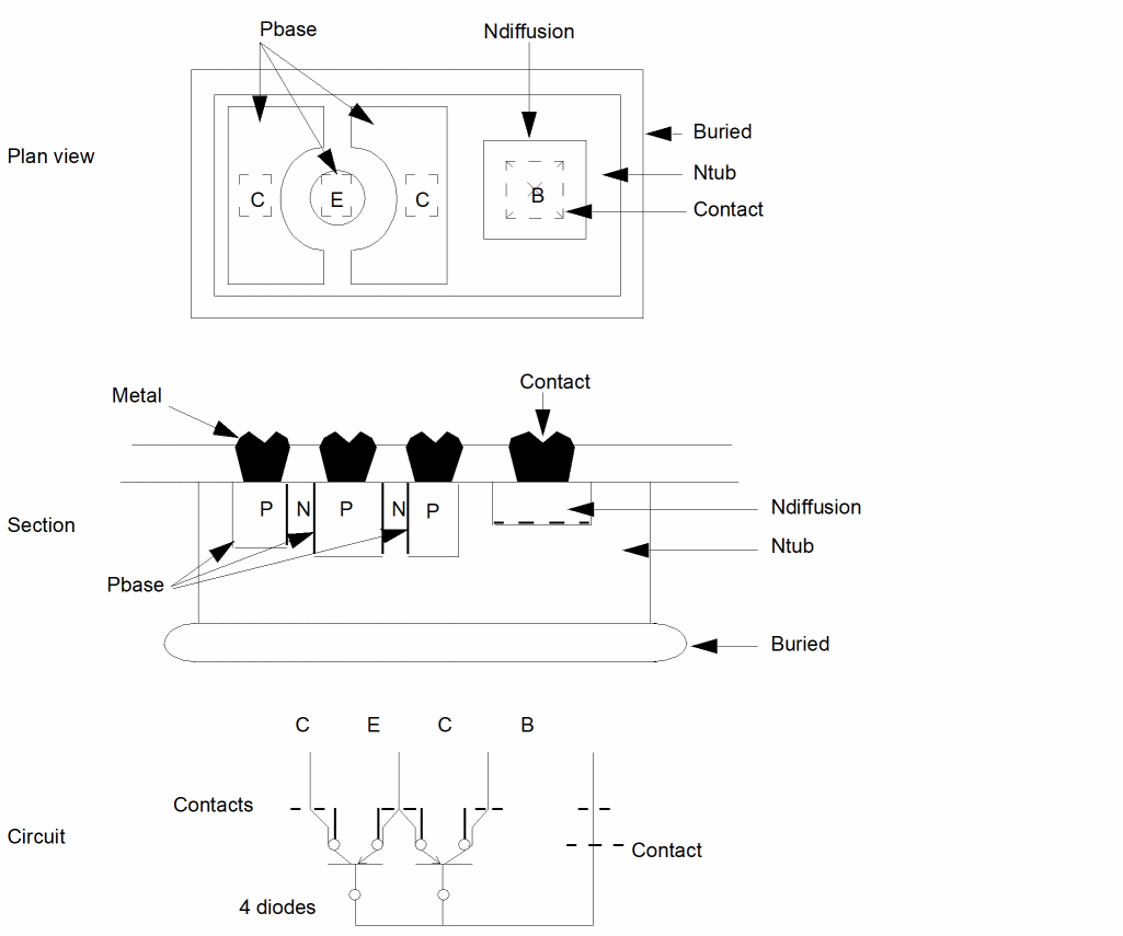
The second difference between the two transistors is that the pnp terminals have a lateral relationship, and the npn terminals have a vertical relationship. This can best be seen in the previous example.
In this example, the buried layer can be used to represent the device, in which case the result is a two-collector pnp transistor. Regardless of the number of collectors, a single transistor is recognized. Each permutation of collectors must be represented in the system device library for the extraction to be performed successfully. Problems arise when multiple transistors are created in a single tub. The designer considers such transistors as separate devices having a common base, whereas the program device recognition using the buried layer generates a single device having multiple emitters, and collectors which also appear in the library.
To overcome this problem, use one of two solutions:
- Create another layer for device recognition so that multiple transistors inside a single tub are recognized as such. Each transistor can have multiple collectors.
- Use the collector layer for device recognition resulting in multiple single-collector transistors.
In the first solution, you need a layer that currently does not exist. In the second solution, you need a way to relate the collectors laterally to the emitter.
The same basic technique is used for both solutions. Create a layer which is the oversize of the emitter. Use enough sizing to ensure that the resultant shape interacts with the collectors. The sequences of operations for both solutions are
1   emit = geomGetTexted( Pbase "text" "emit" )
2   Pbasei = geomAndNot( Pbase emit )
3   pnp = geomSize(emit 3 )
4   contb = geomAndNot( Ndiff Pbase )
5   contn = geomAnd( contact Ndiff )
6   contp = geomAnd( contact Pbasei )
7   conte = geomAnd( contact emit )
8   geomConnect(via ( contn metal ndiff )
      via ( contb ndiff buried )
      via ( contp metal Pbasei )
      via ( conte metal emit )
9   extractDevice( pnp emit ("E") Pbasei ( "C" "C" )
      buried ("B") "pnp-2" )
In this example, the oversized emitter is used directly as the device recognition polygon. It interacts, forming collector terminals, with all Pbase that is within the sizing distance of the emitter. In this case, the distance chosen was 3 units. Any Pbase region beyond that distance is not considered as a collector of that device.
Lines 1 to 3 identify the emitter, remove it from the Pbase interconnect, and size it to produce the device recognition polygon. Lines 4 and 5 recognize the two contacts to the buried layer in the same way as for npn. But in this case, the connection is to the base rather than to the collector. Line 6 recognizes the contact to the general Pbase interconnect Pbasei, which in this example represents only the collectors, though it can be used as general interconnect. Line 7 recognizes the contact to the emitter. The geomConnect statement in line 8 ensures the correct connections from metal to all the other interconnect layers. The device statement in line 9 is structured in exactly the same way as the npn device except that one terminal (the collector) has two terminals.
The model name references a device which has two collectors. If other pnp transistors in the circuit have other numbers of collectors, then a separate device statement needs to be used for each to identify the correct library model. There is no processing penalty for having multiple definitions of a single device since all devices with the same recognition layer are processed in a single pass of the data.
1    emit = geomGetTexted( Pbase "text" "emit" )
2    Pbasei = geomAndNot( Pbase emit )
3    bridge = geomSize( emit 3 )
4    pnp = geomStraddle( Pbasei bridge )
5    contb = geomAndNot( ndiff Pbase )
6    contn = geomAnd( contact ndiff )
7    contp = geomAnd( contact Pbasei )
8    conte = geomAnd( contact emit )
9    geomConnect( via ( contn metal ndiff )
       via ( contb ndiff buried )
       via ( contp metal Pbasei )
       via ( conte metal bridge )
10   extractDevice( pnp bridge ("E") Pbasei ("C") buried
       ("B") "pnp" )
In this example, the oversized emitter polygon is used as the emitter terminal of the transistor and as a connectivity bridge from the emitter terminal to the emitter Pbase, which defines the connectivity to the metal.
Lines 1 to 3 identify the emitter, remove it from the Pbase interconnect, and size it to produce the emitter terminal. Lines 4 to 9 are similar to the previous example and define the contacts and connectivity. Line 10 defines the device, differs from the previous example, and requires one collector terminal. The library model referenced is the “standard” three-terminal pnp transistor. Since all pnp devices recognized by this definition has a single collector, this is the only model required in the library. This differs from many models (two collector, three collector) required by the previous example.
Resistor Terminal Recognition
Normally, the specification of device terminals in the extractDevice statement is simple. The layer forming the terminal is defined, and the program automatically forms a terminal from any relationship between the device recognition polygon and that layer.
The specification of resistors and some other devices is not as simple. The two problems are as follows:
- The two ends of a resistor can be terminated in different ways which need different terminal layers. Any single resistor can have any combination of those terminal types.
- A resistor can be terminated by a contact to an interconnect layer.
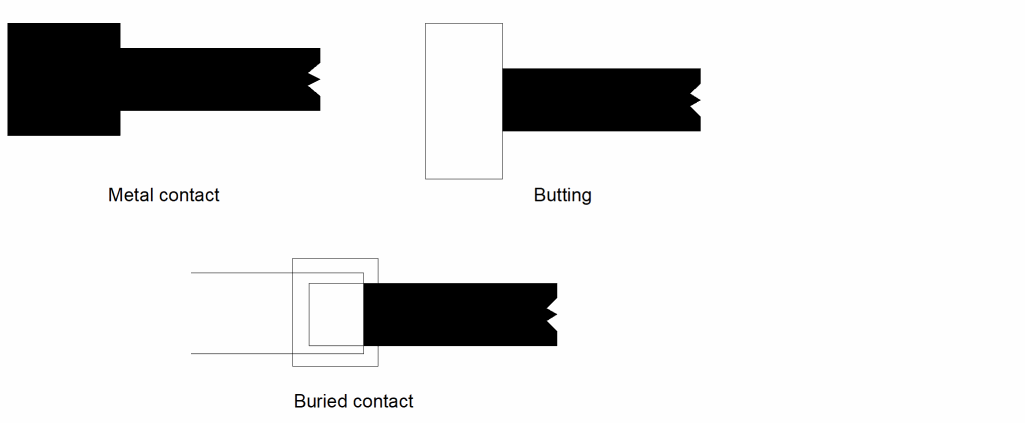
The first problem occurs because a resistor can be terminated in several ways, such as butting an interconnect layer of the same material as the resistor, contacting interconnect metal with a normal metal contact cut, and in the case of a polysilicon resistor, contacting diffusion with a buried contact. Any resistor can have any combination of these terminations, so specifying a “poly interconnect” terminal does not find both terminals of a resistor with one end contacted to metal.
The next example illustrates three ways of terminating a resistor.
The second problem involves the operation of the geomConnect statement. A terminal of a device must be an interconnect layer. This means it must have been defined in a geomConnect statement, which relates a series of interconnect layers by a contact layer, or by a command which propagates that connectivity. If a resistor is formed from the polysilicon layer, the shape forming that device must be removed from that layer to create the interconnecting polysilicon.
All resistors are shorted out by the layer that forms them. In this case, the contact has no polysilicon interconnect to connect to and is badly formed. In addition, there is no interconnect layer to form the terminal. If the metal was used, all metal crossing resistors is connected to the resistor.
The solution offered here is not necessarily the only one, but it does solve both problems at the same time.
The contact structures are separated from the resistor structure, where a dummy shape is generated on the interconnect layer to act as the resistor terminal. This is best described by an example. Consider the case of a resistor which can have its ends terminated by a metal contact or by butting polysilicon interconnect. The resistor is differentiated from the interconnect by a text string of res on the layer textlayer. This example does not consider “buried contacts.” The line numbers in the following commands are for reference only and are not part of the file.
1   resistor = geomGetTexted( polysilicon "textlayer"
               "res" )
2   polyr = geomAndNot( polysilicon resistor )
3   stubs =geomAnd( resistor contact )
4   polyi = geomOr( polyr stubs )
5   geomConnect( via( contact polyi metal ) )
6   extractDevice( resistor polyi ( "PLUS" "MINUS" )
      "resistor" )
Line 1 identifies the resistor from among the polysilicon shapes and line 2 removes it from that layer, leaving polyr. Line 3 copies all contacts that are over the resistor onto layer stubs. Line 4 merges these stubs with the main polysilicon, polyr, to form the final polysilicon interconnect layer, polyi.
The geomConnect statement in line 5 can now successfully make a connection through the contact that was over the resistor. The connection is from one part of the polyi, which was polyr to the other part of polyi which was stubs. The connectivity is now complete without involving the resistor. Both types of terminal on the resistor now relate to the polysilicon interconnect layer polyi, one through direct butting and one through overlap with the part of the interconnect that was derived from the contact.
Line 6 recognizes the device with just a single terminal type. If “buried contacts” had been involved also, additional lines can be added to treat that contact in exactly the same way as the metal contact, leaving the device statement exactly as shown.
The next example illustrates the layer relationships involved for the metal contact to the resistor.
Extraction Device Library Entries
The device recognition facility in Diva’s LPE program requires the definition of a device model. For each device recognized, an instance of that device is placed in the extracted cellview. The cellview type of the device instance is symbol by default. If that extracted cellview is going to be used within LVS, a cellview must be available for that device to correctly netlist. The choice of which cellviews to use for the netlist is achieved through the SI switching and stopping specifications. You might be able to use the SPICE cellviews for this purpose. In many cases, they netlist correctly for LVS; in some cases, they do not. In the case of schematics that contain the device “cap,” the switching is incorrect for LVS because a cap has a SPICE cellview but contains an instance of a capacitor, which also has a SPICE cellview.
The safest cellview type for LVS is lvs. Each of the low-level devices in the system device library has an lvs cellview. The netlisting properties of these cellviews are compatible with the LVS nlpglobals cellview (called lvs) and netlist correctly. The SI switching and stopping lists for the following cellviews needs to be defined.
simNlpGlobalLibName = "basic"
lvsLayoutViewList = list( "lvs" "schematic" "symbolic" )
lvsSchmaticViewList = list( "lvs" "schematic" "gate.sch"
                            "cmos.sch" )
lvsLayoutStopList = list( "lvs" )
lvsSchematicStopList = list( "lvs" )
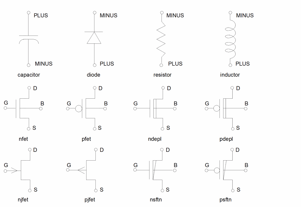
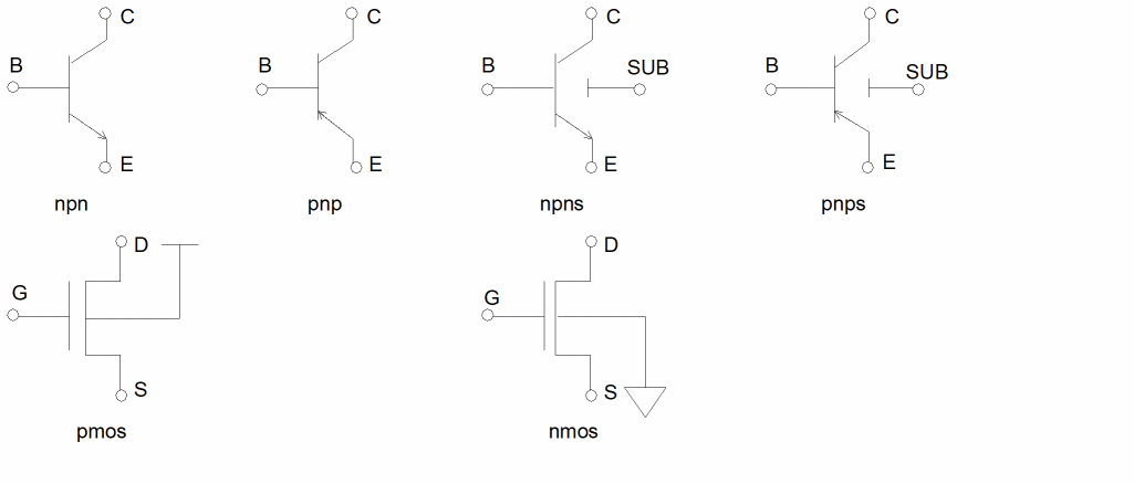
The next example illustrates the symbol representations for the devices having lvs cellviews. The pmos and nmos devices are schematics that reference the nfet and pfet devices, are shown here for clarity, and are considered low level. Note that they have their back-gate connected to ground and power respectively. They must not be used when their back-gate is connected to any other signal.
Substrate, Background, and Ground
This section clarifies the concepts of substrate, background, and ground with regard to the connectivity of a circuit being extracted.
Concepts
The graphics editor has a layer called bkgnd that identifies the complete area of the circuit. The layer color forms the background to the layout, and, when active, the layer can be used to select shapes on all layers. Diva’s LPE program uses the same name, bkgnd, to represent a single polygon whose size encompasses all other shapes in the layout. The background layer can be manipulated as any other graphics layer, but does not have to be created by you.
Substrate is used to represent the physical material underlying the circuitry of the chip. Generally, the substrate is considered to completely encompass the physical circuit and pass beneath all structures. In some technologies, the substrate is subdivided into different areas to represent different electrical functions. For example, in CMOS, the substrate can be divided into well and substrate.
Ground is a name applied to those parts of the circuit which conduct current at ground potential (which can be whatever potential you declare it to be).
Relationships
The main purpose of Diva’s LPE bkgnd layer is to represent the substrate of the circuit in cases where the substrate takes part in the electrical connectivity. It can be subdivided, as in the CMOS example, by the normal layer manipulation commands geomAnd, geomAndNot, and so forth. In some cases, the substrate can be connected to ground, so the bkgnd becomes part of the ground net. In this case, bkgnd, substrate, and ground are synonymous. Substrate can be connected instead to any other net or potential of the circuit. Except in those cases where commands are used to subdivide the bkgnd into separate pieces, any nets of the circuit connected to it (via a geomConnect statement) are shorted together.
A measureParasitic statement, generating parasitic devices can use bkgnd as a terminal for the parasitics. This is accomplished by using the layer bkgnd in this way.
cap = measureParasitic( area( polysilicon over bkgnd over
                       aluminum) two_net )
The bkgnd must be connected. Although both polysilicon and aluminum are interconnect layers, the polysilicon and the bkgnd are used as the device terminals because they are the first two interconnect layers from left to right in the statement. If the bkgnd is connected to the circuit by a contact (such as a substrate contact), then one terminal of the parasitic devices is connected to that net. If there is no real connection to bkgnd, then all the parasitics are connected together to a common net. This net has no connection to the remainder of the circuit and is totally independent of any net in the circuit.
This measureParasitic statement has a different result.
cap = measureParasitic( area (polysilicon) two_net )
In this example, there is no second interconnect layer to which the parasitic device can be connected, so the program generates a new, unique net to connect to one of the parasitic terminals. One terminal is connected to the polysilicon net and the other to a single net, which is common to all parasitic devices generated this way. This unique net is not, and cannot be, connected to the remainder of the circuit. It is independent of any net in the circuit.
Return to top