1
LEF Syntax
This chapter contains information about the following topics:
- About Library Exchange Format Files
-
LEF Statement Definitions
- Bus Bit Characters
- Clearance Measure
- Divider Character
- Extensions
- FIXEDMASK
- Layer (Cut)
- Layer (Implant)
- Layer (Masterslice or Overlap)
- Layer (Routing)
- Library
- Macro
- Layer Geometries
- Macro Obstruction Statement
- Macro Pin Statement
- Manufacturing Grid
- Maximum Via Stack
- Nondefault Rule
- Property Definitions
- Site
- Units
- Use Min Spacing
- Version
- Via
- Via Rule
- Via Rule Generate
About Library Exchange Format Files
A Library Exchange Format (LEF) file contains library information for a class of designs. Library data includes layer, via, placement site type, and macro cell definitions. The LEF file is an ASCII representation using the syntax conventions described in “Typographic and Syntax Conventions”.
General Rules
Note the following information about creating LEF files:
- Identifiers like net names and cell names are limited to 2,048 characters.
- Distance is specified in microns.
-
Distance precision is controlled by the
UNITSstatement. -
LEF statements end with a semicolon (
;). You must leave a space between the last character in the statement and the semicolon.
Character Information
For information, see Character Information in the DEF Syntax chapter.
Name Escaping Semantics for LEF/DEF Files
For information, see Name Escaping Semantics for Identifiers in the DEF Syntax chapter.
Managing LEF Files
You can define all of your library information in a single LEF file; however this creates a large file that can be complex and hard to manage. Instead, you can divide the information into two files, a “technology” LEF file and a “cell library” LEF file.
A technology LEF file contains all of the LEF technology information for a design, such as placement and routing design rules, and process information for layers. A technology LEF file can include any of the following LEF statements:
     [VERSION statement]
[BUSBITCHARS statement]
[DIVIDERCHAR statement]
[UNITS statement]
[MANUFACTURINGGRID statement]
[USEMINSPACING statement]
[CLEARANCEMEASURE statement ;]
[PROPERTYDEFINITIONS statement]
[FIXEDMASK ;]
[LAYER (Nonrouting) statement
 | LAYER (Routing) statement] ...
[MAXVIASTACK statement]
[VIA statement] ...
[VIARULE statement] ...
[VIARULE GENERATE statement] ...
[NONDEFAULTRULE statement] ...
[SITE statement] ...
[BEGINEXT statement] ...
[END LIBRARY]
A cell library LEF file contains the macro and standard cell information for a design. A library LEF file can include any of the following statements:
     [VERSION statement]
[BUSBITCHARS statement]
[DIVIDERCHAR statement]
[VIA statement] ...
[SITE statement]
[MACRO statement
  [PIN statement] ...
  [OBS statement ...] ] ...
[BEGINEXT statement] ...
[END LIBRARY]
When reading in LEF files, always read in the technology LEF file first.
Order of LEF Statements
LEF files can contain the following statements. You can specify statements in any order; however, data must be defined before it is used. For example, the UNITS statement must be defined before any statements that use values that are dependent on UNITS values, LAYER statements must be defined before statements that use the layer names, and VIA statements must be defined before referencing them in other statements. If you specify statements in the following order, all data is defined before being used.
     [VERSION statement]
[BUSBITCHARS statement]
[DIVIDERCHAR statement]
[UNITS statement]
[MANUFACTURINGGRID statement]
[USEMINSPACING statement]
[CLEARANCEMEASURE statement ;]
[PROPERTYDEFINITIONS statement]
[FIXEDMASK ;]
[  LAYER (Nonrouting) statement
 | LAYER (Routing) statement] ...
[MAXVIASTACK statement]
[VIARULE GENERATE statement] ...
[VIA statement] ...
[VIARULE statement] ...
[NONDEFAULTRULE statement] ...
[SITE statement] ...
[MACRO statement
  [PIN statement] ...
  [OBS statement ...]] ...
[BEGINEXT statement] ...
[END LIBRARY]
LEF Statement Definitions
The following definitions describe the syntax arguments for the statements that make up a LEF file. Statements are listed in alphabetical order, not in the order they should appear in a LEF file. For the correct order, see “Order of LEF Statements”.
Bus Bit Characters
[BUSBITCHARS"delimiterPair" ;]
Specifies the pair of characters used to specify bus bits when LEF names are mapped to or from other databases. The characters must be enclosed in double quotation marks. For example:
BUSBITCHARS "[]" ;
If one of the bus bit characters appears in a LEF name as a regular character, you must use a backslash (\) before the character to prevent the LEF reader from interpreting the character as a bus bit delimiter.
If you do not specify the BUSBITCHARS statement in your LEF file, the default value is “[]”.
Clearance Measure
[CLEARANCEMEASURE {MAXXY | EUCLIDEAN} ;]
Defines the clearance spacing requirement that will be applied to all object spacing in the SPACING and SPACINGTABLE statements. If you do not specify a CLEARANCEMEASURE statement, euclidean distance is used by default.
|
Uses the largest x or y distances for spacing between objects. |
|
|
Uses the euclidean distance for spacing between objects. That is, the square root of x2 + y2. |
Divider Character
[DIVIDERCHAR "character" ;]
Specifies the character used to express hierarchy when LEF names are mapped to or from other databases. The character must be enclosed in double quotation marks. For example:
DIVIDERCHAR "/" ;
If the divider character appears in a LEF name as a regular character, you must use a backslash (\) before the character to prevent the LEF reader from interpreting the character as a hierarchy delimiter.
If you do not specify the DIVIDERCHAR statement in your LEF file, the default value is “/”.
Extensions
[BEGINEXT “tag”extension
ENDEXT]
Adds customized syntax to the LEF file that can be ignored by tools that do not use that syntax. You can also use extensions to add new syntax not yet supported by your version of LEF/DEF, if you are using version 5.1 or later.
Specifies the contents of the extension.
Identifies the extension block. You must enclose tag in double quotation marks (“”).
Example 1-1 Extension Statement
BEGINEXT “1VSI Signature 1.0”
CREATOR “company name”
DATE “timestamp”
REVISION “revision number”
ENDEXT
Here, tag is 1VSI Signature 1.0 and extension is all the remaining text before ENDEXT, including any newline characters. In this example, the extension string is as follows:
CREATOR “company name”
DATE “timestamp”
REVISION “revision number”
FIXEDMASK
[FIXEDMASK ;]
Does not allow mask shifting. All the LEF macro pin mask assignments must be kept fixed and cannot be shifted to a different mask. The LEF macro pin shapes should all have MASK assignments, if FIXEDMASK is present. In addition, macro OBS should all have MASK assignments unless they have SPACING override. This statement should be included before the LAYER statements.
...
MANUFACTURINGGRID 0.001 ;
FIXEDMASK ;
LAYER xxx
Some technologies do not allow mask shifting for cells using multi-mask patterning. For example, the pin and routing shapes are all pre-colored and must not be shifted to other masks.
Layer (Cut)
Defines cut layers in the design. Each cut layer is defined by assigning it a name and design rules. You must define cut layers separately, with their own layer statements. For details, see the following chapter:
Layer (Implant)
Defines implant layers in the design. Each layer is defined by assigning it a name and simple spacing and width rules. For details, see the following chapter:
Layer (Masterslice or Overlap)
Defines masterslice (non-routing) or overlap layers in the design. For details, see the following chapter:
Layer (Routing)
Defines routing layers in the design. Each layer is defined by assigning it a name and design rules. You must define routing layers separately, with their own layer statements. For details, see the following chapter:
Library
Defining Library Properties to Create 32/28 nm and Smaller Nodes Rules
You can include library properties in your LEF file to create 32/28 nm and smaller nodes rules that currently are not supported by existing LEF syntax. The properties are specified inside the PROPERTYDEFINITIONS statements.
All properties use the following syntax within the LEF PROPERTYDEFINITIONS statement:
PROPERTYDEFINITIONS LAYERpropNameSTRING ["stringValue"] ;
END PROPERTYDEFINITIONS
The property definitions for the library properties are as follows:
PROPERTYDEFINITIONS
LIBRARY LEF58_ANTENNAMAXCUMAREA STRING ;
LIBRARY LEF58_ANTENNAMAXGATEAREA STRING ;
LIBRARY LEF58_ANTENNAMODELGROUP STRING ;
LIBRARY LEF58_CELLEDGESPACINGTABLE STRING ;
LIBRARY LEF58_CELLVARIANTS STRING ;
LIBRARY LEF58_CONSTRAINTLENGTH STRING ;
LIBRARY LEF58_CUTMASKTRACK STRING ;
LIBRARY LEF58_FINFET STRING ;
LIBRARY LEF58_IMPLANTGROUP STRING ;
LIBRARY LEF58_LAYERMASKSHIFT STRING ;
LIBRARY LEF58_MAXFLOATINGAREA STRING ;
LIBRARY LEF58_MAXVIASTACK STRING ;
LIBRARY LEF58_METALWIDTHTRACK STRING ;
LIBRARY LEF58_METALWIDTHVIAMAP STRING ;
LIBRARY LEF58_OALAYERMAP STRING ;
LIBRARY LEF58_PGVIATRACK STRING ;
LIBRARY LEF58_STACKVIALAYERRULE STRING ;
LIBRARY LEF58_STACKVIARULE STRING ;
LIBRARY LEF58_TAPDISTANCE STRING ;
LIBRARY LEF58_TAPDISTANCERULE STRING ;
LIBRARY LEF58_TRIMMETALTRACK STRING ;
LIBRARY LEF58_VOLTAGEMODE STRING ;
END PROPERTYDEFINITIONS
Antenna Maximum Cumulative Area Rule
You can create an antenna maximum cumulative area rule to specify the maximum cumulative area of all layers to gate, which is not connected to the diffusion diode.
You can define an antenna maximum cumulative rule by using the following PROPERTYDEFINITIONS statement:
PROPERTYDEFINITIONS
LIBRARY LEF58_ANTENNAMAXCUMAREA STRING
"ANTENNAMAXCUMAREAvalue[RANGEbottomLayer topLayer]
[CUTLAYERONLY]
;" ;
END PROPERTYDEFINITIONS
Antenna Maximum Cumulative Area Rule Example
-
The following rule means that the antenna is only measured on the cut layers,
VIA5 - VIA7, on the given layer range.PROPERTYDEFINITIONS
LIBRARY LEF58_ANTENNAMAXCUMAREA STRING
ANTENNAMAXCUMAREA 100.00 RANGE M5 M8 CUTLAYERONLY ; " ;
END PROPERTYDEFINITIONS
Antenna Maximum Gate Area Rule
You can create an antenna maximum gate area rule to specify the maximum total area of all the antenna gate areas connected on any routing layer on the given antenna model.
You can define an antenna maximum gate area rule by using the following PROPERTYDEFINITIONS statement:
PROPERTYDEFINITIONS
LIBRARY LEF58_ANTENNAMAXGATEAREA STRING
"ANTENNAMAXGATEAREA {OXIDE1 | OXIDE2 | OXIDE3 | OXIDE4 | OXIDE5
| ... | OXIDE32}max_area
; " ;
END PROPERTYDEFINITIONS
Antenna Model Group Rule
You can define an antenna model group rule by using the following PROPERTYDEFINITIONS statement:
PROPERTYDEFINITIONS
LIBRARY LEF58_ANTENNAMMODELGROUP STRING
   "ANTENNAMODELGROUP OXIDEx MODEL {OXIDEy}...[GATEONLY]
      ;" ;
END PROPERTYDEFINITIONS
Antenna Model Group Rule Examples
-
The following rule means that if two pins are electrically connected with pin1 having model
OXIDE1and pin2 having modelOXIDE2,OXIDE3by combiningOXIDE1andOXIDE2would be checked while the individualOXIDE1andOXIDE2models would be ignored.PROPERTYDEFINITIONS
LIBRARY LEF58_ANTENNAMODELGROUP STRING “
ANTENNAMODELGROUP OXIDE3 MODEL OXIDE1 OXIDE2 ; ” ;
END PROPERTYDEFINITIONS
-
The following rule indicates that if two pins are electrically connected with pin1 having model
OXIDE1and pin2 having modelOXIDE2,OXIDE1andOXIDE2would be checked separately whileOXIDE4would be ignored because not all of the models in the model group are connected.PROPERTYDEFINITIONS
LIBRARY LEF58_ANTENNAMODELGROUP STRING “
ANTENNAMODELGROUP OXIDE4 MODEL OXIDE1 OXIDE2 OXIDE3 ; ” ;
END PROPERTYDEFINITIONS
-
The following rule indicates that if three pins are electrically connected with pin1 having model
OXIDE1, pin2 having modelOXIDE2and pin3 having modelOXIDE3,OXIDE4by combiningOXIDE1andOXIDE2is checked along withOXIDE3, which does not belong to any model group. The individualOXIDE1andOXIDE2models are ignored.PROPERTYDEFINITIONS
LIBRARY LEF58_ANTENNAMODELGROUP STRING “
ANTENNAMODELGROUP OXIDE4 MODEL OXIDE1 OXIDE2 ; ” ;
END PROPERTYDEFINITIONS
-
The following rule indicates that if two pins are electrically connected with pin1 having model
OXIDE1andOXIDE3and pin2 having modelOXIDE2andOXIDE4,OXIDE5by combiningOXIDE1andOXIDE2andOXIDE6by combiningOXIDE3andOXIDE4would only be checked separately.PROPERTYDEFINITIONS
LIBRARY LEF58_ANTENNAMODELGROUP STRING “
ANTENNAMODELGROUP OXIDE5 MODEL OXIDE1 OXIDE2 ;
ANTENNAMODELGROUP OXIDE6 MODEL OXIDE3 OXIDE4 ; ” ;
END PROPERTYDEFINITIONS
-
The following illustration is an example of the rule below.
PROPERTYDEFINITIONS
LIBRARY LEF58_ANTENNAMODELGROUP STRING “
ANTENNAMODELGROUP OXIDE3 MODEL OXIDE1 OXIDE2 ; ” ;
END PROPERTYDEFINITIONS
Figure 1-1 Illustration of the Antenna Model Group Rule
Constraint Length Rule
You can create a constraint length rule to define the horizontal and vertical length of the concatenated constraint area. You can define a constraint length rule by using the following PROPERTYDEFINITIONS statement:
PROPERTYDEFINITIONS LIBRARY LEF58_CONSTRAINTLENGTH STRING "CONSTRAINTLENGTHlength{MAX|MIN} [HORIZONTAL|VERTICAL] [EXCEPTABUTTED] [WIDTHminWidth] CONSTRAINTAREATYPE {typeName| VERTICALCELLEDGESTACK | HORIZONTALCELLEDGESTACK} ;" ;
END PROPERTYDEFINITIONS
Figure 1-2 Illustration of Constraint Length Rule
Figure 1-3 Illustration of Constraint Length Rule with WIDTH
Cell Edge Spacing Table Rule
You can create a cell edge spacing table rule to define a spacing table between two macro edges having different edge types.
This cell edge spacing table must be defined before reading in the MACRO definition with defined EDGETYPE in cell LEF files.
You can define a cell edge spacing table rule by using the following PROPERTYDEFINITIONS statement:
PROPERTYDEFINITIONS
LIBRARY LEF58_CELLEDGESPACINGTABLE STRING
    "CELLEDGESPACINGTABLE [NODEFAULT]
      {EDGETYPE {edgeType1 | DEFAULT}
      {edgeType2 | DEFAULT} [EXCEPTABUTTED]
            [EXCEPTNONFILLERINBETWEEN]
            [OPTIONAL | SOFT | EXACT] spacing} ...
      ;...” ;
END PROPERTYDEFINITIONS
Cell Edge Spacing Table Rule Examples
-
The following rule indicates that:
-
0.1 µm is the spacing between a macro edge with type
GROUP1and a macro edge with typeGROUP2. Abutting the two macros is also allowed. -
0.2 µm is the optional spacing between two macro edges with type
GROUP1; a certain placement option controls whether or not it is honored. -
0.3 µm is the spacing between a macro edge with type
GROUP2and a macro edge without a type. -
0.4 µm is the soft spacing between two macro edges with type
GROUP2, which would be ignored if placement quality is impacted too much. -
0.5 µm spacing is not allowed between a macro edge with type
GROUP1and a macro edge without a type. -
The rest of the combination of edges,
DEFAULTtoDEFAULT, do not have any spacing constraint, or 0.0 µm.
PROPERTYDEFINITIONS
  LIBRARY LEF58_CELLEDGESPACINGTABLE STRING
    "CELLEDGESPACINGTABLE
        EDGETYPE GROUP1 GROUP2 EXCEPTABUTTED 0.1
        EDGETYPE GROUP1 GROUP1 OPTIONAL 0.2
        EDGETYPE GROUP2 DEFAULT 0.3
        EDGETYPE GROUP2 GROUP2 SOFT 0.4; ";
        EDGETYPE GROUP1 DEFAULT EXACT 0.5; ";
END PROPERTYDEFINITIONS
-
0.1 µm is the spacing between a macro edge with type
-
The following rule illustrates the cell edge spacing rule for the given macro definition:
PROPERTYDEFINITIONS
  LIBRARY LEF58_CELLEDGESPACINGTABLE STRING
    "CELLEDGESPACINGTABLE
        EDGETYPE GROUP1 GROUP1 0.001 ; “ ;
END PROPERTYDEFINITIONS
Figure 1-4 Illustration of Cell Edge Spacing Rule
-
The following rule illustrates a cell edge spacing rule with
EXCEPTNONFILLERINBETWEEN:PROPERTYDEFINITIONS LIBRARY LEF58_CELLEDGESPACINGTABLE STRING "CELLEDGESPACINGTABLE EDGETYPE E1 E1 EXCEPTNONFILLERINBETWEEN 1.5; " ; END PROPERTYDEFINITIONS
Figure 1-5 Illustration of Cell Edge Spacing Rule withEXCEPTNONFILLERINBETWEEN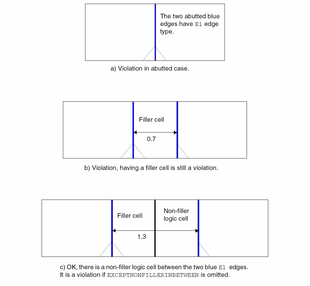
Cell Variants Rule
You can create a cell variants rule to specify the placement locations of electrically equivalent (EEQ) cells.
You can define a cell variants rule by using the following PROPERTYDEFINITIONS statement:
PROPERTYDEFINITIONS
LIBRARY LEF58_CELLVARIANTS STRING
"CELLVARIANTSvariantTotalNum
[STARTVARIANTstartVariant[XFLIPSTARTVARIANTstartVariant]]
YFLIPMAP {flippedVariantNumsiteVariantNum}...
[XFLIPMAP {cellVariantNum siteVariantNum}... ]
;" ;
END PROPERTYDEFINITIONS
-
The following example illustrates the cell variant rule:
PROPERTYDEFINITIONS
LIBRARY LEF58_CELLVARIANTS STRING "
CELLVARIANTS 3 YFLIPMAP 1 1 2 3 3 2 ; " ;
END PROPERTYDEFINITIONS
...
MACRO A
...
END A
MACRO A2
PROPERTY LEF58_EEQ " EEQ A VARIANT 2 ; " ;
...
END A2
MACRO A3
PROPERTY LEF58_EEQ " EEQ A VARIANT 3 ; " ;
...
END A3
Figure 1-6 Illustration of the Cell Variants Rule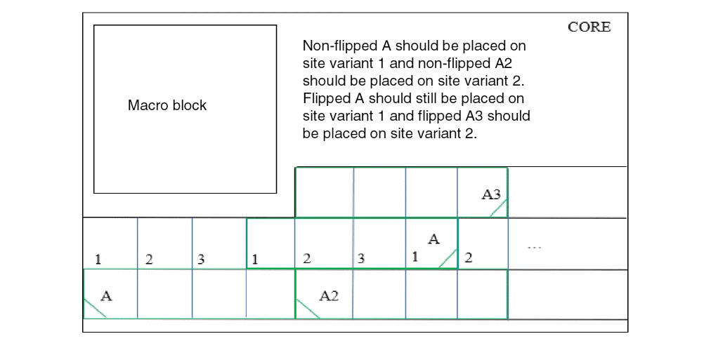
-
The following example illustrates a cell variant rule with
XFLIPMAP:LIBRARY LEF58_CELLVARIANTS STRING "
CELLVARIANTS 4 STARTVARIANT 1 XFLIPSTARTVARIANT 2
YFLIPMAP { 1 2 2 1 3 2 4 1 } XFLIPMAP { 1 0 2 0 3 1 4 2 } ; “ ;
END PROPERTYDEFINITIONS
Figure 1-7 Illustration of the Cell Variants Rule with XFLIPMAP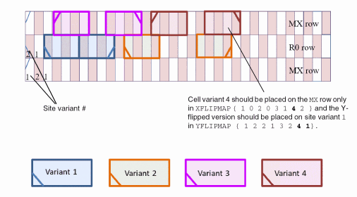
-
The following example illustrates a cell variant rule with
XFLIPMAP:LIBRARY LEF58_CELLVARIANTS STRING "
CELLVARIANTS 4 STARTVARIANT 1 XFLIPSTARTVARIANT 2
YFLIPMAP { 1 2 2 1 3 2 4 1 } XFLIPMAP { 1 0 2 0 3 1 4 2 } ; “ ;
END PROPERTYDEFINITIONS
Figure 1-8 Illustration of the Cell Variants Rule with XFLIPMAP
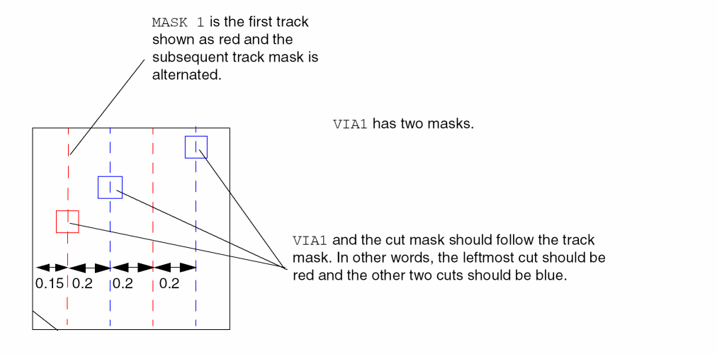
Cut Mask Track Rule
You can create a cut mask track rule to specify a preferred cut mask vertical track for the mask of the cell master cuts.
You can define a cut mask rule by using the following PROPERTYDEFINITIONS statement:
PROPERTYDEFINITIONS
LIBRARY LEF58_CUTMASKTRACK STRING
“CUTMASKTRACKcutLayerMASKmaskNumOFFSEToffsetPITCHpitch;” ;
END PROPERTYDEFINITIONS
The following example indicates that the preferred cut mask vertical track for the mask of the cell master cuts is mask 1:
PROPERTYDEFINITIONS
LIBRARY LEF58_CUTMASKTRACK STRING "
CUTMASKTRACK VIA1 MASK 1 OFFSET 0.15 PITCH 0.2
      ; ";
END PROPERTYDEFINITIONS
Figure 1-9 Illustration of the Cut Mask Track Rule
FinFET Rule
You can create a FinFET rule to specify the FinFET pitch to be pitch.
You can define a FinFET rule by using the following PROPERTYDEFINITIONS statement:
PROPERTYDEFINITIONS
LIBRARY LEF58_FINFET STRING
"FINFET
PITCHpitch[OFFSEToffset] {HORIZONTAL|VERTICAL}
[NOCORECELL]
;" ;
END PROPERTYDEFINITIONS
The following example indicates that the FinFET y pitch is 0.108 µm:
PROPERTYDEFINITIONS
LIBRARY LEF58_FINFET STRING "
FINFET
PITCH 0.108 HORIZONTAL ; ";
END PROPERTYDEFINITIONS
Implant Group Rule
You can create an implant group rule to specify rules that apply for all the shapes on an implant layer.
You can define an implant group rule by using the following PROPERTYDEFINITIONS statement:
PROPERTYDEFINITIONS
LIBRARY LEF58_IMPLANTGROUP STRING
"IMPLANTGROUPgroupName
LAYER {layerName}... BASEDLAYERbasedLayerName;" ;
END PROPERTYDEFINITIONS
PROPERTYDEFINITIONS
LIBRARY LEF58_IMPLANTGROUP STRING “
       IMPLANTGROUP GROUP1 LAYER VT1 VT2 BASEDLAYER VT1 ;
       IMPLANTGROUP GROUP2 LAYER VT1 VT3 BASEDLAYER VT1 ; “ ;
END PROPERTYDEFINITIONS
In this example, the combined shapes on VT1 and VT2 and the combined shapes on VT1 and VT3 must follow the rules on VT1.
Layer Mask Shift Rule
You can create a layer mask shift rule to specify that mask could be shifted on the given layers.
You can define a layer mask shift rule by using the following PROPERTYDEFINITIONS statement:
PROPERTYDEFINITIONS LIBRARY LEF58_LAYERMASKSHIFT STRING "LAYERMASKSHIFTlayer1[layer2...] [MACROCLASS { RING | BLOCK | PAD | CORE | ENDCAP }...] ;" ;
END PROPERTYDEFINITIONS
Layer Mask Shift Rule Examples
-
The following example indicates that mask-shifting is allowed on LEF layer
M1andVIA1but not on other layers:PROPERTYDEFINITIONSLIBRARY LEF58_LAYERMASKSHIFT STRING "LAYERMASKSHIFT M1 VIA1 ; " ;END PROPERTYDEFINITIONS -
The following example indicates that mask-shifting is allowed on the LEF layer
M1andVIA1onMACROwith classCOREorENDCAPbut not on other layers and macros with other classes. In addition,FIXEDMASKonMACRO Ameans that mask-shifting onMACRO Ais not allowed on all layers:PROPERTYDEFINITIONSLIBRARY LEF58_LAYERMASKSHIFT STRING "LAYERMASKSHIFT M1 VIA1 MACROCLASS CORE ENDCAP ; “ ;END PROPERTYDEFINITIONSMACRO ACLASS CORE ;FIXEDMASK ;...END A
Maximum Floating Area Rule
Maximum area rules exist for floating metal shapes that are not connected to a diffusion or polysilicon gate. Similar to process antenna rules, maximum floating area rules apply only to the current layer and any lower layers (that is, all layers that have been fabricated up to the layer of interest). Maximum floating area rules can be used to avoid shorts between floating and non-floating metal wires that are caused by arcing due to charge buildup during processing steps.
You can create a global maximum floating area rule by using the following PROPERTYDEFINITIONS statement:
PROPERTYDEFINITIONS
LIBRARY LEF58_MAXFLOATINGAREA STRING
"MAXFLOATINGAREAmaxArea
{SINGLELAYER | CONNECTED | ALLCONNECTED}minRoutingLayermaxRoutingLayer
[[LAYERSminRoutingLayermaxRoutingLayer]
SPACINGminSpacing[PARSPACINGminParSpacingminParallelLength...]] ... ;" ;
END PROPERTYDEFINITIONS
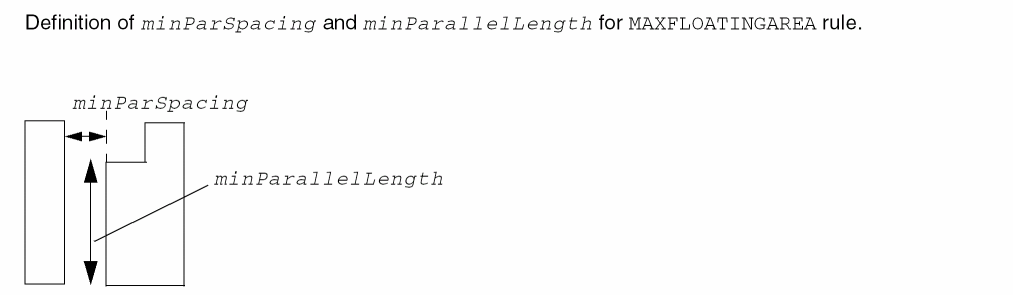
Maximum Floating Area Rule Examples
-
Example 1
Assume the following rule exists:PROPERTYDEFINITIONS LIBRARY LEF58_MAXFLOATINGAREA STRING “MAXFLOATINGAREA 1000 SINGLELAYER m1 m6 SPACING 1.0 ;” ; END PROPERTYDEFINITIONS
Every shape on layers m1 to m6 with maximum floating area greater than 1000 μm2 must have spacing of greater than or equal to 1.0 μm to any grounded metal. -
Example 2
Assume the following rule exists:PROPERTYDEFINITIONS LIBRARY LEF58_MAXFLOATINGAREA STRING “MAXFLOATINGAREA 1000 CONNECTED m1 m6 LAYERS m1 m1 SPACING 1.0 PARSPACING 0.5 0.8 0.2 2.0 LAYERS m2 m6 SPACING 0.6 PARSPACING 0.3 0.9 ;” ; END PROPERTYDEFINITIONS
For layer m1, any floating metal must be either greater than or equal to 1.0 μm distance from grounded metal, or:- If it is greater than or equal to 0.5 μm distance away, there must be at least 0.8 μm of parallel length at the minimum spacing.
- If it is greater than or equal to 0.2 μm distance away, there must be at least 2.0 μm of parallel length at the minimum spacing.
Spacing that is less than 0.2 μm is not allowed.
Any floating m2 through m6 shapes with area that is greater than 1000 μm2, must either be greater than or equal to 0.6 μm distance from grounded metal, or they must be greater than or equal to 0.3 μm distance away with greater than or equal to 0.9 μm of parallel length.
See Figure 1-9 for different layout examples using this rule.
Figure 1-10 Maximum Floating Area Rule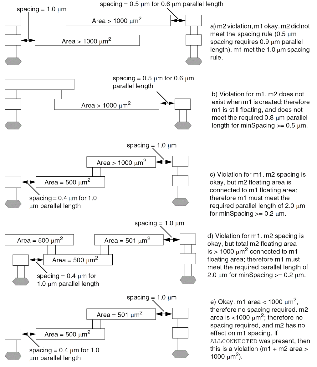
Maximum Via Stack Rule
You can create a maximum via stack rule to require a series of stacked vias to all be multi-cut vias. A via is considered to be in a stack with other vias if the cuts of all the vias partially overlap (the boolean AND of the cut layer shapes from every via in the stack is not empty). A multi-cut via interrupts the stack, unless the NOSINGLE keyword is specified.
If multiple MAXVIASTACK statements are defined, all of them must be fulfilled individually.
You can define a maximum via stack rule using the following PROPERTYDEFINITIONS statement:
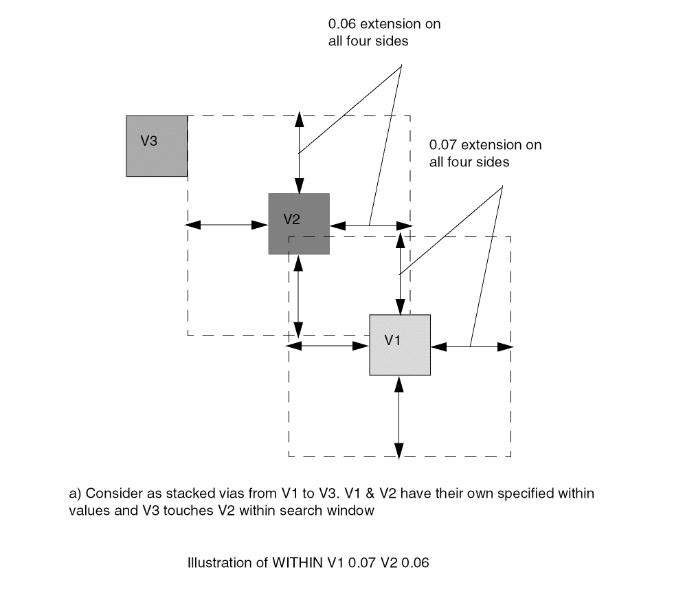
PROPERTYDEFINITIONS LIBRARY LEF58_MAXVIASTACK STRING "MAXVIASTACKmaxStack[SAMENET] [NOSINGLE] [IGNOREONESAMEMETALcutWithin] [MINMULTICUTnumCut] [WITHIN {LOWCUTSIZE | {cutLayerName within[CENTERTOCENTER]}...} | CENTERCUTWITHINcutLayerName belowCutWithin aboveCutWithin] [EXCEPTPGNET] [EXCEPTAREAindividualArea sumArea] [RANGEbottomLayer topLayer] [EXCEPTCUTCLASSLIST {cutLayer cutClassName}...] [[NOVIALIST {viaName}...]... |[NOCUTCLASSLIST {cutLayer cutClassName}...]...] ;" ;
END PROPERTYDEFINITIONS
|
Specifies that the maximum via stack rule applies only when all of the cuts below a cut on cutLayerName must be within belowCutWithin of that cut and all of the cuts above a cut on cutLayerName must be within aboveCutWithin of that cut. The maximum via stack rule must be defined such that having a cut on cutLayerName is the only way to violate the rule. For example, if a maximum via stack number of |
|
|
Specifies that the within distance between two cuts on adjacent cut layers is measured in the center-to-center style. |
|
|
Specifies that the rule does not apply if the metal shape containing the stacked vias has an area greater than or equal to individualArea on any layer except the bottommost and topmost metal layers of the stacked vias or the union sum of those metal areas is greater than or equal to sumArea.
If any stacked via larger than the specified maximum number in the rule does not qualify for the exemptions in |
|
|
Specifies that the rule is exempted for any vias belonging to the given cut class cutClassName on the given layer cutLayer. This means that those vias would interrupt a stack as if the vias did not exist for this max via stack rule. |
|
|
Specifies that the rule is exempted for power or ground net. |
|
|
Specifies that if the cuts within cutWithin have the same metal on at least one metal layer, they are considered multi-cuts, which interrupt the via stack. However, the bottommost stacked via can consider a same-metal cut only on the routing layer above, and the topmost stacked via can consider a same-metal cut only on the routing layer below. |
|
|
Specifies the maximum number of single-cut vias that are allowed on top of each other (that is, in one continuous stack). |
|
|
Specifies the minimum multi-cut number to be greater than or equal to numCut in order to be a multi-cut exemption to a stacked via violation with number of vias greater than or equal to maxStack. If |
|
|
Specifies that the given cut classes, which belong to the given cutClassName on the given cut layer cutLayer, are not allowed for stacking although the number of cut classes specified in |
|
|
Indicates that any single-cut via in a stack that is larger than maxStack is a violation, and multi-cut vias do not interrupt a stack. Therefore, any stack larger than maxStack must consist of all multi-cut vias. |
|
|
Specifies that the given list of vias in |
|
|
Specifies a range of routing layers for which the maximum stacked via rule applies. If you do not specify a range, the maxStack value applies for all routing layers. The bottomLayer and topLayer values are routing layer names. The specified topLayer layer must be above the layer specified for bottomLayer. |
|
|
Specifies that an object is considered as a stacked via if the upper adjacent layer cut is within the minimum cut size of multiple |
|
Maximum Via Stack Rule Examples
-
If the following rule exists:
Only three single-cut vias can be stacked between layers m1 and m6. See Figure 1-10 for different layout examples using this rule.PROPERTYDEFINITIONS LIBRARY LEF58_MAXVIASTACK STRING “MAXVIASTACK 3 RANGE m1 m6 ;” ; END PROPERTYDEFINITIONS
Figure 1-11 Max Via Stack Rule Examples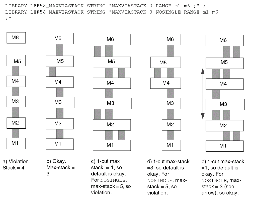
-
The following rule applies if metal shapes containing the stacked vias have an area less than the individual area of 0.1 on any layer:
PROPERTYDEFINITIONS
  LIBRARY LEF58_MAXVIASTACK STRING
    “MAXVIASTACK 2 EXCEPTAREA 0.1 0.15
        RANGE M2 M6 ; ” ;
END PROPERTYDEFINITIONS
Figure 1-12 Illustration of Max Via Stack Rule with EXCEPTAREA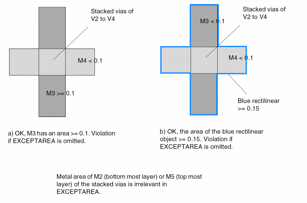
-
The following property rule illustrates
WITHINLOWCUTSIZEwithV1layer:PROERPTY LEF58_CUTCLASS “CUTCLASS ... WIDTH 0.06 ... ; CUTCLASS ... WIDTH 0.12 ... ; ” ;
Figure 1-13 Illustration of Max Via Stack Rule with WITHIN LOWCUTSIZEFigure 1-14 Illustration of Max Via Stack Rule with WITHIN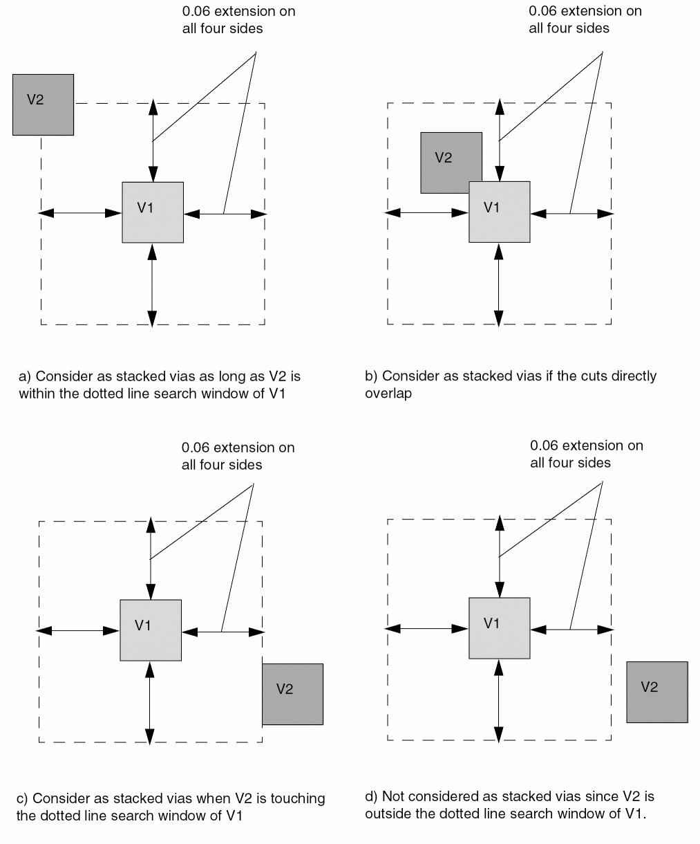
-
The following property rule illustrates the max via stack rule with
NOVIALIST:PROPERTYDEFINITIONS LIBRARY LEF58_MAXVIASTACK STRING “ MAXVIASTACK 3 NOVIALIST V1B V2C ; “ ; END PROPERTYDEFINITIONS
Figure 1-15 Illustration of Max Via Stack Rule with NOVIALIST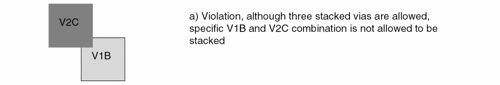
-
The following property rule illustrates multiple max via stack rules:
PROPERTYDEFINITIONS
     LIBRARY LEF58_MAXVIASTACK STRING “
          MAXVIASTACK 2 RANGE M1 M5 ;
          MAXVIASTACK 3 RANGE M3 M7 ; “ ;
END PROPERTYDEFINITIONS
Figure 1-16 Illustration of Multiple Max Via Stack Rules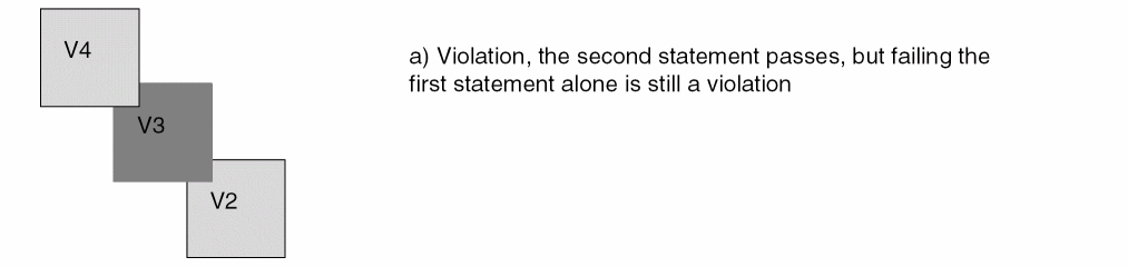
-
The following example illustrates the max via stack rule with
CENTERCUTWITHIN:PROPERTYDEFINITIONS LIBRARY LEF58_MAXVIASTACK STRING “ MAXVIASTACK 3 CENTERCUTWITHIN V3 0.000 0.020 RANGE M1 M5 ; ” ; END PROPERTYDEFINITIONS
Figure 1-17 Illustration of Max Via Stack Rule with CENTERCUTWITHIN
-
The following property rule illustrates a max via stack rule with
EXCEPTCUTCLASSLIST:PROPERTYDEFINITIONS LIBRARY LEF58_MAXVIASTACK STRING “ MAXVIASTACK 2 EXCEPTCUTCLASSLIST V2 V2C; ” ; END PROPERTYDEFINITIONS
Figure 1-18 Illustration of Max Via Stack Rule with EXCEPTCUTCLASSLIST
Metal Width Track Rule
You can create a metal width track rule to define the preferred routing direction for tracks on a specified layer.
You can define a metal width track rule by using the following PROPERTYDEFINITIONS statement:
PROPERTYDEFINITIONS
LIBRARY LEF58_METALWIDTHTRACK STRING
“METALWIDTHTRACKroutingLayerCOREOFFSEToffset{WIDTHwidthPITCHpitch[REPEATrepeat]}...
;” ;
END PROPERTYDEFINITIONS
Metal Width Track Rule Example
-
The following example is an illustration of the metal track width rule:
LAYER M1TYPE ROUTING ;DIRECTION HORIZONTAL ;...END M1...LIBRARY LEF58_METALWIDTHTRACK STRING“METALWIDTHTRACK M1 COREOFFSET 0.15WIDTH 0.2 PITCH 0.4WIDTH 0.1 PITCH 0.2 REPEAT 4WIDTH 0.1 PITCH 0.4 ; “ ;END PROPERTYDEFINITIONS
Figure 1-19 Illustration of Metal Track Width Rule
Metal Width Via Map Rule
You can create a metal width via map rule to specify the vias to be used based on the given width values of the below and above metal layers.
You can define a metal width via map rule by using the following PROPERTYDEFINITIONS statement:
PROPERTYDEFINITIONS
LIBRARY LEF58_METALWIDTHVIAMAP STRING
   "METALWIDTHVIAMAP
       [USEVIACUTCLASS]
       {VIA viaLayer
          {belowLayerWidth aboveLayerWidth
          |belowLayerLowWidth belowLayerHighWidth
             aboveLayerLowWidth aboveLayerHighWidth}
          viaName [PGVIA]}...
       ;..." ;
END PROPERTYDEFINITIONS
Metal Width Via Map Rule Examples
-
The following example indicates that
V1_SMALLshould be used on cut layerV1for below metal width of 0.05 and above metal width of 0.08 wires whileV1_LARGEshould be used for below metal width of 0.07 and above metal width of 0.08 wires:PROPERTYDEFINITIONS LIBRARY LEF58_METALWIDTHVIAMAP STRING “ METALWIDTHVIAMAP VIA V1 0.05 0.08 V1_SMALL VIA V1 0.07 0.08 V1_LARGE; ” ; END PROPERTYDEFINITIONS
OpenAccess Layer Map Rule
You can create an OpenAccess layer map rule to define equivalence between LEF and OpenAccess layers and also between the geometries and shapes placed on the layers.
You can define an OpenAccess layer map rule by using the following PROPERTYDEFINITIONS statement:
PROPERTYDEFINITIONS
LIBRARY LEF58_OALAYERMAP STRING
“OALAYERMAPoaLayer{ [PURPOSEoaPurpose] BLOCKAGElayer| LAYERlayer[MASKmaskNum] }
;...” ;
END PROPERTYDEFINITIONS
Here, LEF58_OALAYERMAP can contain multiple mapping statements, separated by ‘;’. The property syntax allows two variants of the statement:
OpenAccess Layer Map Rule Examples
-
The following example indicates that the LEF layer
M1is mapped to OpenAccess layerMetal1:PROPERTYDEFINITIONS LIBRARY LEF58_OALAYERMAP STRING “ OALAYERMAP Metal1 LAYER M1 ; “ ; END PROPERTYDEFINITIONS
-
The following example indicates that the LEF
MASK 1shapes onM1would go to OpenAccess layerMetal1AwhileMASK2 shapes onM1would go to OpenAccess layerMetal1B:PROPERTYDEFINITIONS
LIBRARY LEF58_OALAYERMAP STRING “
     OALAYERMAP Metal1A LAYER M1 MASK 1 ;
     OALAYERMAP Metal1B LAYER M1 MASK 2 ; “ ;
END PROPERTYDEFINITIONS
PG Via Track Rule
You can use a PG via track rule to define vertical tracks for aligning all of the power and ground cell vias on a specified layer of a cell macro with the ALIGNPGVIATOTRACK property.
You can define a PG via track rule by using the the following PROPERTYDEFINITIONS statement:
PROPERTYDEFINITIONS
LIBRARY LEF58_PGVIATRACK STRING
“PGVIATRACKcutLayerCOREOFFSEToffsetPITCHpitch; “ ;
END PROPERTYDEFINITIONS
The following example is an illustration of the PG via track rule:
PROPERTYDEFINITIONS
LIBRARY LEF58_PGVIATRACK STRING “
          PGVIATRACK VIA1 COREOFFSET 0.15
               PITCH 0.2 ; “ ;
END PROPERTYDEFINITIONS
Figure 1-20 Illustration of the PG Via Track Rule
Stack Via Layer Rule
You can use a stack via layer rule to define stack via rules on individual layers. These rules are combined to form a stack via rule.
You can define a stack via layer rule by using the following PROPERTYDEFINITIONS statement:
PROPERTYDEFINITIONS
LIBRARY LEF58_STACKVIALAYERRULE STRING
“STACKVIALAYERRULEruleNameLAYERcutLayerName[CUTCLASSclassName]
ROWCOLnumCutRows numCutCols[XPITCHxPitch[MAXXPITCHmaxXPitch]]
[YPITCHyPitch[MAXYPITCHmaxYPitch]]
[BELOWMINLENGTHbelowMinLength]
[ABOVEMINLENGTHaboveMinLength]
[MAXCELLEXTENSIONextensionPitch]
[OFFGRIDCUT]
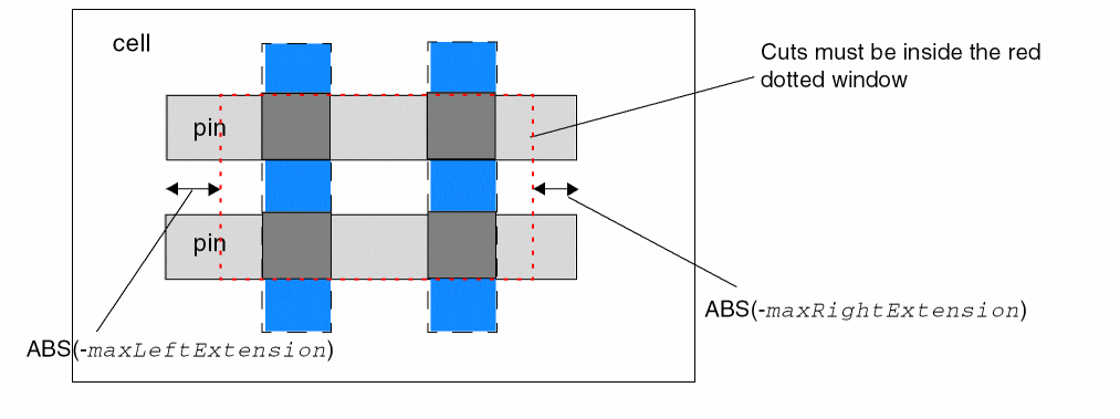
[MAXXLINEENDmaxLeftExtensiion maxRightExtension]
[MAXYLINEENDmaxBottomExtensiion maxTopExtension]
; “ ;
END PROPERTYDEFINITIONS
-
The following example is an illustration of the stack via layer rule:
PROPERTY LEF58_STACKVIALAYERRULE “STACKVIALAYERRULE SVLR1 LAYER VIA1 CUTCLASS VA1ROWCOL 2 3 XPITCH 2 YPITCH 3 ;STACKVIALAYERRULE SVLR2 LAYER VIA2 CUTCLASS VA2ROWCOL 2 2 XPITCH 3 YPITCH 3BELOWMINLENGTH 0.3 ; “ ;PROPERTY LEF58_STACKVIARULE “STACKVIARULE SVR1 SVLR1 SVLR2 ; “ ;
Figure 1-21 Illustration of Stack Via Layer RulesFigure 1-22 Illustration of MAXCELLEXTENSION extensionPitch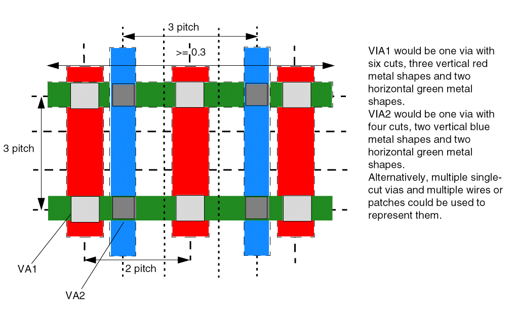 Figure 1-23 Illustration of OFFGRIDCUT
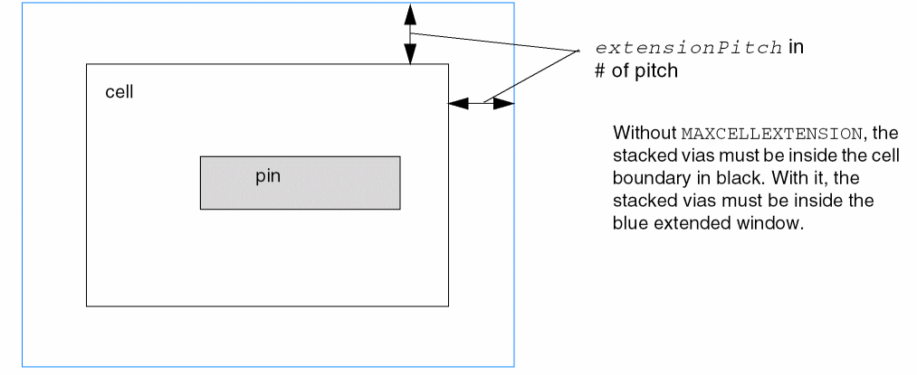 Figure 1-24 Illustration of MAXXLINEEND with Negative Values for maxLeftExtension and maxRightExtension
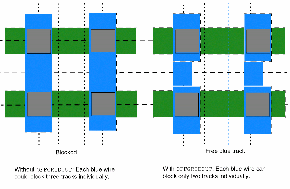
Stack Via Rule
You can create a stack via rule to specify a list of stack via rules for individual layers.
You can define a stack via rule by using the following PROPERTYDEFINITIONS statement:
PROPERTYDEFINITIONS
LIBRARY LEF58_STACKVIARULE STRING
“STACKVIARULEruleName{stackLayerRuleName}...[EMFACTORemFactor]
; “ ;
END PROPERTYDEFINITIONS
Tap Distance Rule
You can create a tap distance rule to specify distance between well tap cells.
You can define a tap distance rule by using the following PROPERTYDEFINITIONS statement:
PROPERTYDEFINITIONS
LIBRARY LEF58_TAPDISTANCE STRING
“TAPDISTANCE {distance| TAPDISTANCERULEruleName|{HALFROWrowNum[LEFT|RIGHT]{distance| TAPDISTANCERULEruleName}}...}
TAPTYPEtypeName; “ ;
END PROPERTYDEFINITIONS
-
The following example is an illustration of the tap distance rule:
PROPERTYDEFINITIONSLIBRARY LEF58_TAPDISTANCE STRING “ TAPDISTANCE HALFROW 1 2.4 HALFROW 2 2.0 TAPTYPE TAP1 TAPDISTANCE HALFROW 1 1.2 HALFROW 2 1.2 HALFROW 3 LEFT 0 HALFROW 3 RIGHT 0.8 HALFROW 4 LEFT 0 HALFROW 4 RIGHT 0.8 TAPTYPE TAP2 ; “ ; END PROPERTYDEFINITIONS
Figure 1-25 Illustration of Tap Distance Rule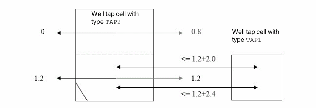
Tap Distance Rule Property
You can create a tap distance rule property to specify effective tap distance.
You can define a tap distance rule property by using the following PROPERTYDEFINITIONS statement:
PROPERTYDEFINITIONS
LIBRARY LEF58_TAPDISTANCERULE STRING
“TAPDISTANCERULEruleNameDEFAULTdistance[LAYERlayerName layerDistance]...
     ; ”;
END PROPERTYDEFINITIONS
Trim Metal Track Rule
You can create a trim metal track rule to define the trim metal tracks on a trim layer.
You can define a trim metal track rule by using the following PROPERTYDEFINITIONS statement:
PROPERTYDEFINITIONS LIBRARY LEF58_TRIMMETALTRACK STRING “TRIMMETALTRACKtrimLayer[GROUPgroupName] [ONTRACK [HALFINFILLER | HALFNONMERGED] [INCLUDELINEEND [TRIMCENTER]]] [MASKmaskNum|METALTRACKOFFSETtrackNumberMETALTRACKPITCHtrackPitch] COREOFFSEToffsetPITCHpitch;” ;
END PROPERTYDEFINITIONS
Trim Metal Track Rule Examples
-
Consider the following example:
LAYER TM1
     TYPE MASTERSLICE ;
     MASK 2 ;
     PROPERTY LEF58_TYPE “TYPE TRIMMETAL ; ” ;
     PROPERTY LEF58_TYPE “TYPE TRIMMEDMETAL M1 ; ” ;
... END TM1...LAYER M1 TYPE ROUTING ; DIRECTION VERTICAL ; ... END M1...
PROPERTYDEFINITIONS LIBRARY LEF58_TRIMMETALTRACK STRING “
The above example means that the trim metal layer ofTM1has two sets of horizontal tracks onMASK 1with starting y locations of0.01and0.12with respect to the origin of the core with repeatable pitch of0.2, and it has another two sets of horizontal tracks onMASK 2with starting y locations of0.08and0.19with respect to the origin of the core with repeatable pitch of0.2. -
The following example is an illustration of the trim metal track rule with
METALTRACKOFFSETandMETALTRACKPITCH:TRIMMETALTRACK TM1 METALTRACKOFFSET 1 METALTRACKPITCH 3 COREOFFSET O1 PITCH P ;TRIMMETALTRACK TM1 METALTRACKOFFSET 2 METALTRACKPITCH 3 COREOFFSET O2 PITCH P ;TRIMMETALTRACK TM1 METALTRACKOFFSET 3 METALTRACKPITCH 3 COREOFFSET O3 PITCH P ;
Figure 1-26 Illustration of Trim Metal Track Rule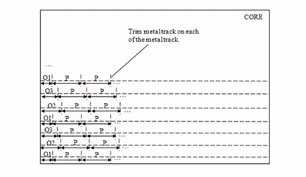
Voltage Mode Rule
You can create a voltage mode rule to define how voltage should be computed in VOLTAGESPACING spacing.
You can define a voltage mode rule by using the following PROPERTYDEFINITIONS statement:
PROPERTYDEFINITIONS
LIBRARY LEF58_VOLTAGEMODE STRING
“VOLTAGEMODE ABSOLUTE
     ; “ ;
END PROPERTYDEFINITIONS
|
Specifies that the absolute maximum voltage of a net is used to define which |
|
Macro
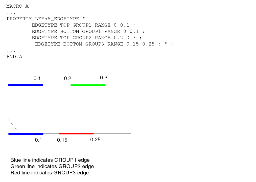
MACROmacroName[CLASS { COVER [BUMP] | RING | BLOCK [BLACKBOX | SOFT] | PAD [INPUT | OUTPUT |INOUT | POWER | SPACER | AREAIO] | CORE [FEEDTHRU | TIEHIGH | TIELOW | SPACER | ANTENNACELL | WELLTAP] | ENDCAP {PRE | POST | TOPLEFT | TOPRIGHT | BOTTOMLEFT | BOTTOMRIGHT} } ;] [FIXEDMASK ;] [FOREIGNforeignCellName[pt[orient]] ;] ... [ORIGINpt;] [EEQmacroName;] [SIZEwidthBYheight;] [SYMMETRY {X | Y | R90} ... ;] [SITEsiteName[sitePattern] ;] ... [PINstatement] ... [OBSstatement] ... [DENSITYstatement] ... [PROPERTYpropNamepropVal;] ... [PROPERTY LEF58_ACCESSAREA "ACCESSAREA {LAYERlayerNameRECTpt pt[CUTCLASSclassName] [EXCEPTEXTRACUT]}... ; " ;] [PROPERTY LEF58_ALIGNPGVIATOTRACK "ALIGNPGVIATOTRACK ; " ;] [PROPERTY LEF58_ALLPINSCONNECTED "ALLPINSCONNECTED ; " ;] [PROPERTY LEF58_CLASS "CLASS {COVER [BUMP | FILL] | RING | BLOCK [BLACKBOX | SOFT] | PAD [INPUT | OUTPUT | INOUT | POWER | SPACER | AREAIO] | CORE [FEEDTHRU | TIEHIGH | TIELOW | SPACER | ANTENNACELL | WELLTAP [TAPWALL] [TAPTYPEtypeName]] | ENDCAP {PRE | POST | TOPLEFT | TOPRIGHT | BOTTOMLEFT | BOTTOMRIGHT | TOPEDGE | BOTTOMEDGE | LEFTEDGE | RIGHTEDGE | LEFTEVENSITEEDGE | LEFTODDSITEEDGE | RIGHTEVENSITEEDGE | RIGHTODDSITEEDGE | LEFTTOPEDGE | RIGHTTOPEDGE | LEFTBOTTOMEDGE | RIGHTBOTTOMEDGE | LEFTTOPEVENSITEEDGE | LEFTTOPODDSITEEDGE | RIGHTTOPEVENSITEEDGE | RIGHTTOPODDSITEEDGE | LEFTBOTTOMEVENSITEEDGE | LEFTBOTTOMODDSITEEDGE | RIGHTBOTTOMEVENSITEEDGE | RIGHTBOTTOMODDSITEEDGE | LEFTTOPCORNER | RIGHTTOPCORNER | LEFTBOTTOMCORNER | RIGHTBOTTOMCORNER | LEFTTOPEVENSITECORNER | LEFTTOPODDSITECORNER | RIGHTTOPEVENSITECORNER | RIGHTTOPODDSITECORNER | LEFTBOTTOMEVENSITECORNER | LEFTBOTTOMODDSITECORNER | RIGHTBOTTOMEVENSITECORNER | RIGHTBOTTOMODDSITECORNER | LEFTEDGETOPBORDER | LEFTEDGEBOTTOMBORDER | RIGHTEDGETOPBORDER | RIGHTEDGEBOTTOMBORDER | LEFTTOPEDGENEIGHBOR | RIGHTTOPEDGENEIGHBOR | LEFTBOTTOMEDGENEIGHBOR | RIGHTBOTTOMEDGENEIGHBOR | LEFTTOPCORNERNEIGHBOR | RIGHTTOPCORNERNEIGHBOR | LEFTBOTTOMCORNERNEIGHBOR | RIGHTBOTTOMCORNERNEIGHBOR | LEFTCORNERTOPBORDER | RIGHTCORNERTOPBORDER | LEFTCORNERBOTTOMBORDER | RIGHTCORNERBOTTOMBORDER | TOPCORNEREDGENEIGHBOR | BOTTOMCORNEREDGENEIGHBOR | TSVTOPEDGE | TSVBOTTOMEDGE | TSVLEFTEDGE | TSVRIGHTEDGE | TSVLEFTTOPCORNER | TSVLEFTBOTTOMCORNER | TSVRIGHTTOPCORNER | TSVRIGHTBOTTOMCORNER | TSVLEFTTOPEDGE | TSVLEFTBOTTOMEDGE | TSVRIGHTTOPEDGE | TSVRIGHTBOTTOMEDGE | TSVLEFTTOPEDGENEIGHBOR | TSVRIGHTTOPEDGENEIGHBOR | TSVLEFTBOTTOMEDGENEIGHBOR | TSVRIGHTBOTTOMEDGENEIGHBOR | TSVLEFTTOPCORNERNEIGHBOR | TSVRIGHTTOPCORNERNEIGHBOR | TSVLEFTBOTTOMCORNERNEIGHBOR | TSVRIGHTBOTTOMCORNERNEIGHBOR} [TAPWALL] [TAPTYPEtypeName] } } ; " ;] [PROPERTY LEF58_CONSTRAINTAREATYPE "CONSTRAINTAREATYPEtypeName{RECTpt pt}... ;..." ;] [PROPERTY LEF58_EDGETYPE "EDGETYPE {RIGHT | LEFT | TOP | BOTTOM}edgeType| BOTHSOURCE | SOURCEDRAIN | DRAINSOURCE | BOTHDRAIN | BOTHFLOATING [CELLROWcellRow| HALFROWhalfRow| RANGExLowxHigh] ;..." ;] [PROPERTY LEF58_EEQ "EEQmacroName[VARIANTnum] ;... " ;] [PROPERTY LEF58_FOREIGN "FOREIGNforeignCellName[pt[orient]] [COMPORIENTforeignOrientName{compOrient}...]... ;... " ;] [PROPERTY LEF58_LAYERMASKSHIFT "LAYERMASKSHIFTlayer1[layer2...] ;... " ;] [PROPERTY LEF58_OBSPARTIAL "OBSPARTIAL {LAYER layerName WIDTHwidthSPACINGspacingRECTptpt}... ; " ;] [PROPERTY LEF58_OBSSPACING "OBSSPACING {FULLDRC | MIN |spacing} [LAYERlayerName]... ; " ;] [PROPERTY LEF58_PLACEWITHIN "PLACEWITHINwithinPRLprl{WITH|WITHOUT} LAYER {layerName}... ; " ;] [PROPERTY LEF58_REQ "REQmacroName; " ;] [PROPERTY LEF58_TAPCENTEROFFSET "TAPCENTEROFFSET {offset| {HALFROWrowNum[LEFT|RIGHT]offset}...} ; " ;]
END macroName
Note: The keywords must be specified in the given order. For example if ORIGIN and SITE are both defined, ORIGIN must be specified first.
Specifies the macro type. If you do not specify CLASS, the macro is considered a CORE macro, and a warning prints when the LEF file is read in. You can specify macros of the following types:
|
Macro with data that is fixed to the floorplan and cannot change, such as power routing (ring pins) around the core. The placers understand that A cover macro can be of the following sub-class:
|
|
|
Large macro that has an internal power mesh, and only exposes power-pin shapes that form a ring along the macro boundary. When power stripes are added across the macro, they connect to each side of the ring-pin but do not go inside the ring. The |
|
|
Predefined macro used in hierarchical design. A block macro can have one of the following sub-classes:
|
|
|
I/O pad. A pad can be one of the following types: For an example of a macro pad cell, see Example 1-2. |
|
|
A standard cell used in the core area. A core macro can be one of the following types:
|
|
|
A macro placed at the ends of core rows (to connect with power wiring).
If the library includes only one corner I/O macro, then appropriate
The |
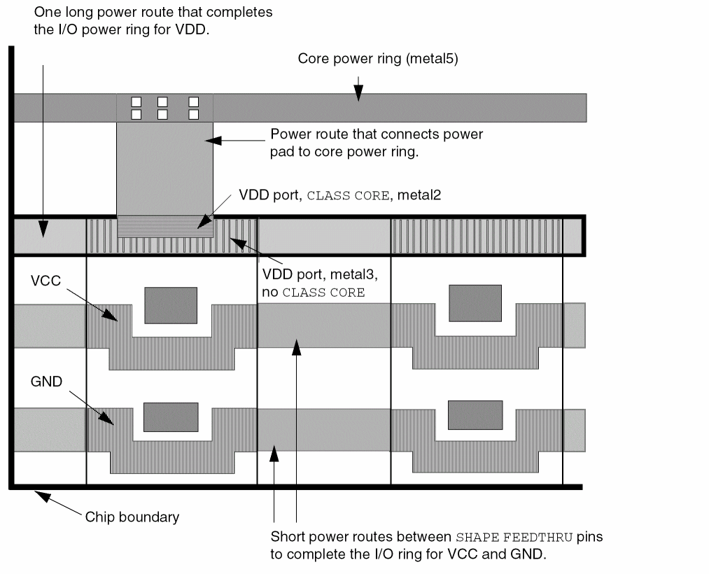
The following example defines a power pad cell that illustrates when to use the CLASS CORE keywords on power ports. For the VDD pin, there are two ports: one to connect to the interior core power ring, and one to complete the I/O power ring. Figure 1-26 illustrates this pad cell.
MACRO PAD_0
CLASS PAD ;
FOREIGN PAD_0 0.000 0.000 ;
ORIGIN 0.000 0.000 ;
SIZE 100.000 BY 300.000 ;
SYMMETRY X Y R90 ;
SITE PAD_SITE ;
# Define pin VDD with SHAPE ABUTMENT because there are no obstructions
# to block a straight connection to the pad rings. The port without
# CLASS CORE is used for completing the I/O power ring.
PIN VDD
DIRECTION INOUT ;
USE POWER ;
SHAPE ABUTMENT ;
PORT
LAYER metal2 ;
RECT 0.000 250.000 100.000 260.000 ;
LAYER metal3 ;
RECT 0.000 250.000 100.000 260.000 ;
END
# Define VDD port with PORT CLASS CORE to indicate that the port connects
# to the core area instead of to the pad ring.
PORT
CLASS CORE ;
LAYER metal2 ;
RECT 0.000 290.000 100.000 300.000 ;
LAYER metal3 ;
RECT 0.000 290.000 100.000 300.000 ;
END
END VDD
# Define pins VCC and GND with SHAPE FEEDTHRU because these pins
# cannot make a straight connection to the pad rings due to obstructions.
PIN VCC
DIRECTION INOUT ;
USE POWER ;
SHAPE FEEDTHRU ;
PORT
LAYER metal2 ;
RECT 0.000 150.000 20.000 160.000 ;
RECT 20.000 145.000 80.000 155.000 ;
RECT 80.000 150.000 100.000 160.000 ;
LAYER metal3 ;
RECT 0.000 150.000 20.000 160.000 ;
RECT 20.000 145.000 80.000 155.000 ;
RECT 80.000 150.000 100.000 160.000 ;
END
END VCC
PIN GND
DIRECTION INOUT ;
USE GROUND ;
SHAPE FEEDTHRU ;
PORT
LAYER metal2 ;
RECT 0.000 50.000 20.000 60.000 ;
RECT 80.000 50.000 100.000 60.000 ;
END
END GND
OBS
LAYER metal1 ;
RECT 0.000 0.000 100.000 300.000 ;
LAYER metal2 ;
RECT 25.000 50.000 75.000 60.000 ;
RECT 30.500 157.000 70.500167.000 ;
END
END PAD_0
Specifies the metal density for large macros.
The DENSITY rectangles on a layer should not overlap, and should cover the entire area of the macro. You can choose the size of the rectangles based on the uniformity of the density of the block. If the density is uniform, a single rectangle can be used. If the density is not very uniform, the size of the rectangles can be specified to be 10 to 20 percent of the density window size, so that any error due to non-uniform density inside each rectangle area is small.
For example, if the metal density rule is for a 100 μm x 100 μm window, the density rectangles can be 10x10 μm squares. Any non-uniformity will have little impact on the density calculation accuracy.
If two adjacent rectangles have the same or similar density, they can be merged into one larger rectangle, with one average density value. The choice between accuracy and abstraction is left to the abstract generator.
The DENSITY syntax is defined as follows:
[DENSITY
{LAYER layerName ;
{RECT x1 y1 x2 y2 densityValue ;} ...
} ...
END] ...
The following statement specifies the density for macro testMacro:
MACRO testMacro
CLASS ...
PIN ...
OBS ...
DENSITY
LAYER metal1 ;
RECT 0 0 100 100 45.5 ; #rect from (0,0) to (100,100), density of 45.5%
RECT 100 0 200 100 42.2 ; #rect from (100,0) to (200, 100), density of 42.2%
END
...
END testMacro
Specifies that the macro being defined should be electrically equivalent to the previously defined macroName. EEQ macros include devices such as OR-gates or inverters that have several implementations with different shapes, geometries, and orientations.
Electrically equivalent macros have the following requirements:
- Corresponding pins must have corresponding functionality.
- Pins must be defined in the same order.
- For each group of corresponding pins (one from each macro), pin function and electrical characteristics must be the same.
- The EEQ macroName specified must refer to a previously defined macro. If the EEQ macroName referenced is already electrically equivalent to other model macros, all referenced macros are considered electrically equivalent.
Indicates that the specified macro does not allow mask-shifting. All the LEF PIN MASK assignments must be kept fixed and cannot be shifted to a different mask to optimize routing density. All the LEF PIN shapes should have MASK assignments, if FIXEDMASK statement is present.
MACRO my_block
CLASS BLOCK ;
FIXEDMASK ;
...
FOREIGN foreignCellName [pt [orient]]
Specifies the foreign (GDSII) structure name to use when placing an instance of the macro. The optional pt coordinate specifies the macro origin (lower left corner when the macro is in north orientation) offset from the foreign origin. The FOREIGN statement has a default offset value of 0 0, if pt is not specified.
The optional orient value specifies the orientation of the foreign cell when the macro is in north orientation. The default orient value is N (North).
Example 1-4 Foreign Statements
The following examples show two variations of the FOREIGN statement. The negative offset specifies that the GDSII structure should be above and to the right of the macro lower left corner.
MACRO ABC ...
FOREIGN ABC -2 -3 ;
The positive offset specifies that the GDSII structure should be below and to the left of the macro lower left corner.
MACRO EFG ...
FOREIGN EFG 2 3 ;
Specifies the name of the library macro.
Defines obstructions on the macro. Obstruction geometries are specified using layer geometries syntax. See “Macro Obstruction Statement” for syntax information.
Specifies how to find the origin of the macro to align with a DEF COMPONENT placement point. If there is no ORIGIN statement, the DEF placement point for a North-oriented macro is aligned with 0, 0 in the macro. If ORIGIN is given in the macro, the macro is shifted by the ORIGIN x, y values first, before aligning with the DEF placement point. For example, if the ORIGIN is 0, -1, then macro geometry at 0, 1 are shifted to 0, 0, and then aligned to the DEF placement point.
Defines pins for the macro. See “Macro Pin Statement” for syntax information.
Specifies a numerical or string value for a macro property defined in the PROPERTYDEFINITIONS statement. The propName you specify must match the propName listed in the PROPERTYDEFINITIONS statement.
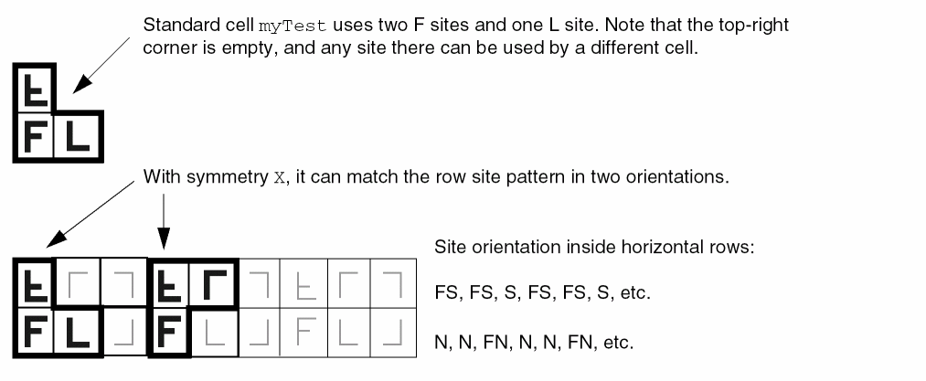
Specifies the site associated with the macro. Normal row-based standard cells only have a single SITE siteName statement, without a sitePattern. The sitePattern syntax indicates that the cell is a gate-array cell, rather than a row-based standard cell. Gate-array standard cells can have multiple SITE statements, each with a sitePattern.
The sitePattern syntax is defined as follows:
[xOrigin yOrigin siteOrient [stepPattern]]
|
Specifies the origin of the site inside the macro. |
|
|
Specifies the orientation of the site at that location. |
If the site is repeated, you can specify a stepPattern that defines the repeating pattern. The stepPattern syntax is defined as follows:
[DO xCount BY yCount STEP xStep yStep]
The following statement defines a macro that uses the sites created in Example 1-17:
MACRO myTest
CLASS CORE ;
SIZE 10.0 BY 14.0 ; #Uses 2 F and 1 L site, is F + L wide, and double height
SYMMETRY X ; #Can flip about the X axis
SITE Fsite 0 0 N ; #The lower left Fsite at 0,0
SITE Fsite 0 7.0 FS ; #The flipped south Fsite above the first Fsite at 0,7
SITE Lsite 4.0 0 N ; #The Lsite to the right of the first Fsite at 4,0
...
PIN ... ;
END myTest
Figure 1-27 illustrates the placement results of this definition.
The following statement includes the gate-array site pattern syntax. It uses two F sites in a row with N (North) orientation.
MACRO myTest
CLASS CORE ;
SIZE 8.0 BY 7.0 ; #Width = 2 * Fsite width, height = Fsite height
SITE Fsite 0 0 N DO 2 BY 1 STEP 4.0 0 ; #Xstep = 4.0 = Fsite width
...
END myTest
This definition produces a cell with the sites shown in Figure 1-28.

Specifies a placement bounding rectangle, in microns, for the macro. The bounding rectangle always stretches from (0, 0) to the point defined by SIZE. For example, given SIZE 10 BY 40, the bounding rectangle reaches from (0, 0) after adjustment due to the ORIGIN statement, to (100, 400).
Placers assume the placement bounding rectangle cannot overlap placement bounding rectangles of other macros, unless OBS OVERLAP shapes are used to create a non-rectangular area.
After placement, a DEF COMPONENTS placement pt indicates where the lower-left corner of the placement bounding rectangle is placed after any possible rotations or flips. The bounding rectangle width and height should be a multiple of the placement grid to allow for abutting cells.
For blocks, the placement bounding rectangle typically contains all pin and blockage geometries, but this is not required. For example, typical standard cells have pins that lie outside the bounding rectangle, such as power pins that are shared with cells in the next row above them.
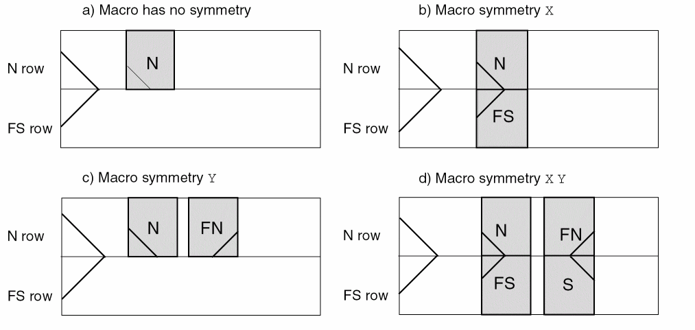
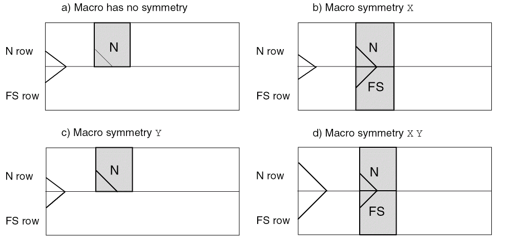
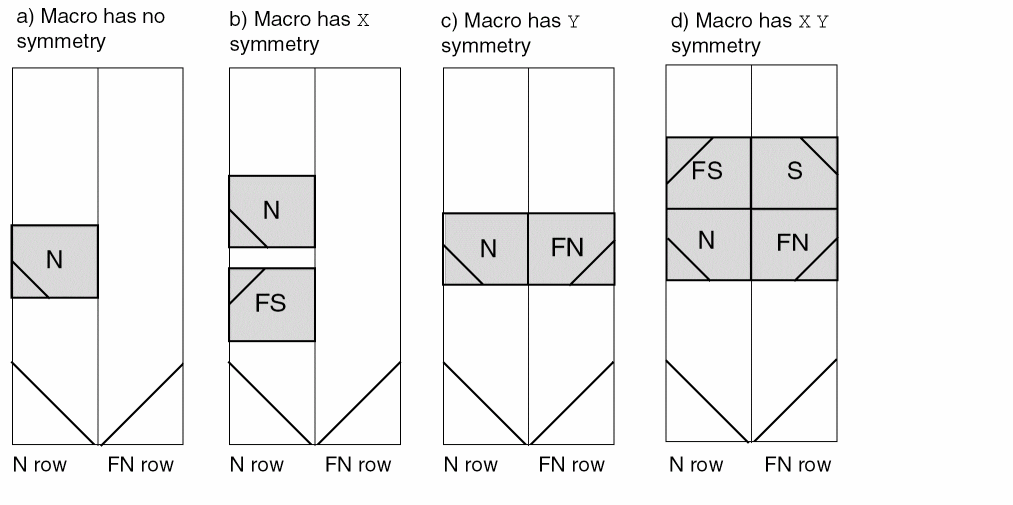
Specifies which macro orientations should be attempted by the placer before matching to the site of the underlying rows. In general, most standard cell macros should have symmetry X Y. N (North) is always a legal candidate. For each type of symmetry defined, additional orientations become legal candidates. For more information on defining symmetry, see “Defining Symmetry”.
Possible orientations include:
For corner I/O pads, if the library includes BOTTOMLEFT, BOTTOMRIGHT, TOPLEFT, and TOPRIGHT I/O corner cells, then they are placed in North orientation (no flipping). However, if the library includes only one type of corner I/O, then SYMMETRY in x and y are required to create the rows for all four of them.
Defining Macro Properties to Create 32/28 nm and Smaller Nodes Rules
You can include macro layer properties in your LEF file to create 32/28 nm and smaller nodes rules that currently are not supported by existing LEF syntax. The properties are specified inside the Macro statements where they can be seen with other rules.
Before you can reference them, properties must be defined at the beginning of the LEF file in the PROPERTYDEFINITIONS statement, immediately before the first Macro statement.
-
Properties belong to the
MACRO/PINobject and have a type ofSTRING. -
The property names used for these rules all start with
LEF58_.
All properties use the following syntax within the LEF PROPERTYDEFINITIONS statement:
PROPERTYDEFINITIONS
MACRO propName STRING ["stringValue"] ;
PIN propName STRING ["stringValue"] ;
END PROPERTYDEFINITIONS
The property definitions for the macro properties are as follows:
PROPERTYDEFINITIONS
MACRO LEF58_ACCESSAREA STRING ;
MACRO LEF58_ALIGNPGVIATOTRACK STRING ;
MACRO LEF58_ALLPINSCONNECTED STRING ;
MACRO LEF58_CLASS STRING ;
MACRO LEF58_CONSTRAINTAREATYPE STRING ;
MACRO LEF58_EDGETYPE STRING ;
MACRO LEF58_EEQ STRING ;
MACRO LEF58_FOREIGN STRING ;
MACRO LEF58_LAYERMASKSHIFT STRING ;
MACRO LEF58_OBSPARTIAL STRING ;
MACRO LEF58_OBSSPACING STRING ;
END PROPERTYDEFINITIONS
Access Area Rule
The access area rule can be used on the macro to specify a via access area on the specified layer.
You can specify the access area rule by using the following property definition:
PROPERTY LEF58_ACCESSAREA"ACCESSAREA {LAYERlayerNameRECTpt pt[CUTCLASSclassName] [EXCEPTEXTRACUT]}... ; " ;
-
The following example means that the cuts of
VIA1ofVAmust be inside1.0 1.0 2.0 2.0and the cuts ofVIA1of the other cut class must be inside1.5 1.5 2.2 2.2when connecting to aM1(below metal layer) pin shape that overlaps with the given area.PROPERTY LEF58_ACCESSAREA " ACCESSAREA LAYER VIA1 RECT 1.0 1.0 2.0 2.0 CUTCLASS VA LAYER VIA1 RECT 1.5 1.5 2.2 2.2 ; " ;
-
The following example means that the cuts of
VIA1ofVAmust be inside1.0 1.0 2.0 2.0when connect to aM1(below metal layer) pin shape that overlaps with the given area and the cuts ofVIA1of the other cut class does not have any restriction.PROPERTY LEF58_ACCESSAREA " ACCESSAREA LAYER VIA1 RECT 1.0 1.0 2.0 2.0 CUTCLASS VA ; " ;
-
The diagram below illustrates the following access area rule:
PROPERTY LEF58_ACCESSAREA “
     ACCESSAREA LAYER VIA1 RECT 1.0 1.0 3.5 1.8
          EXCEPTEXTRACUT
          LAYER VIA1 RECT 6.0 0.5 7.0 1.0
          LAYER VIA1 RECT 6.0 1.8 7.0 2.5 ; “ ;
Figure 1-30 Illustration of the Access Area Rule
Align PG Via to Track Rule
The align PG via to track attribute can be used on the macro to align the power or ground cell vias to the given tracks defined in the PG via track rule in PGTRACKVIA.
You can specify the align PG via to track attribute by using the following property definition:
PROPERTY LEF58_ALIGNPGVIATOTRACK
"ALIGNPGVIATOTRACK
   ;..." ;
|
Specifies that all the power or ground cell vias of this macro should be aligned to the tracks defined in |
||
All Pins Connected Rule
The all pins connected rule can be used to specify that all of the pins in the macro are strongly connected internally.
You can specify the all pins connected rule by using the following property definition:
PROPERTY LEF58_ALLPINSCONNECTED
   "ALLPINSCONNECTED
   ; " ;
|
Specifies that all of the pins in this macro are strongly connected internally. All of the pins should only have one port. This construct could be defined only in a |
||
Class Rule
You can use the class rule to define a macro as a special cover macro for metal filling purpose.
You can create class rule by using the following property definition:
PROPERTY LEF58_CLASS
"CLASS
     {COVER [BUMP | FILL]
     | RING
     | BLOCK [BLACKBOX | SOFT]
     | PAD [INPUT | OUTPUT | INOUT | POWER | SPACER | AREAIO]
     | CORE [FEEDTHRU | TIEHIGH | TIELOW | SPACER | ANTENNACELL
         | WELLTAP [TAPWALL] [TAPTYPE typeName]]
     | ENDCAP {PRE | POST | TOPLEFT | TOPRIGHT | BOTTOMLEFT
         | BOTTOMRIGHT
         | TOPEDGE | BOTTOMEDGE | LEFTEDGE | RIGHTEDGE
         | LEFTEVENSITEEDGE | LEFTODDSITEEDGE
         | RIGHTEVENSITEEDGE | RIGHTODDSITEEDGE
         | LEFTTOPEDGE | RIGHTTOPEDGE
         | LEFTBOTTOMEDGE | RIGHTBOTTOMEDGE
         | LEFTTOPEVENSITEEDGE | LEFTTOPODDSITEEDGE
         | RIGHTTOPEVENSITEEDGE | RIGHTTOPODDSITEEDGE
         | LEFTBOTTOMEVENSITEEDGE | LEFTBOTTOMODDSITEEDGE
         | RIGHTBOTTOMEVENSITEEDGE | RIGHTBOTTOMODDSITEEDGE
         | LEFTTOPCORNER | RIGHTTOPCORNER
         | LEFTBOTTOMCORNER | RIGHTBOTTOMCORNER
         | LEFTTOPEVENSITECORNER | LEFTTOPODDSITECORNER
         | RIGHTTOPEVENSITECORNER | RIGHTTOPODDSITECORNER
         | LEFTBOTTOMEVENSITECORNER
         | LEFTBOTTOMODDSITECORNER
         | RIGHTBOTTOMEVENSITECORNER
         | RIGHTBOTTOMODDSITECORNER
         | LEFTEDGETOPBORDER
         | LEFTEDGEBOTTOMBORDER
         | RIGHTEDGETOPBORDER
         | RIGHTEDGEBOTTOMBORDER
         | LEFTTOPEDGENEIGHBOR
         | RIGHTTOPEDGENEIGHBOR
         | LEFTBOTTOMEDGENEIGHBOR
         | RIGHTBOTTOMEDGENEIGHBOR}
         | LEFTTOPCORNERNEIGHBOR
         | RIGHTTOPCORNERNEIGHBOR
         | LEFTBOTTOMCORNERNEIGHBOR
         | RIGHTBOTTOMCORNERNEIGHBOR
         | LEFTCORNERTOPBORDER
         | RIGHTCORNERTOPBORDER
         | LEFTCORNERBOTTOMBORDER
         | RIGHTCORNERBOTTOMBORDER
         | TOPCORNEREDGENEIGHBOR
         | BOTTOMCORNEREDGENEIGHBOR
         | TSVTOPEDGE | TSVBOTTOMEDGE
         | TSVLEFTEDGE | TSVRIGHTEDGE
         | TSVLEFTTOPCORNER | TSVLEFTBOTTOMCORNER
         | TSVRIGHTTOPCORNER | TSVRIGHTBOTTOMCORNER
         | TSVLEFTTOPEDGE | TSVLEFTBOTTOMEDGE
         | TSVRIGHTTOPEDGE | TSVRIGHTBOTTOMEDGE
         | TSVLEFTTOPEDGENEIGHBOR
         | TSVRIGHTTOPEDGENEIGHBOR
         | TSVLEFTBOTTOMEDGENEIGHBOR
         | TSVRIGHTBOTTOMEDGENEIGHBOR
         | TSVLEFTTOPCORNERNEIGHBOR
         | TSVRIGHTTOPCORNERNEIGHBOR
         | TSVLEFTBOTTOMCORNERNEIGHBOR
         | TSVRIGHTBOTTOMCORNERNEIGHBOR}
         [TAPWALL] [TAPTYPE typeName]
     }
  ; " ;
All other keywords are same as the existing macro CLASS syntax.
-
The following example indicates that macro
Ais a cover macro for metal filling purpose:MACRO APROPERTY LEF58_CLASS “CLASS COVER FILL ; ” ;...END A -
The following example shows four different set of configurations for class rule:
Figure 1-31 Illustration of Class Rule
-
The following example shows the use of
RIGHTEDGE(RE),TOPEDGE(TE),LEFTOPEDGE(LTE)andLEFTTOPCORNER(LTC)endcap cells:-
RIGHTEDGEin N and FS orientation is used in start of rows -
RIGHTEDGEin FN and S orientation is used in end of rows -
TOPEDGEin N orientation is used in bottom row of the core or top row right above a block macro (the first row should have N orientation; otherwise, the bottom FS row would be wasted) -
TOPEDGEin FS orientation is used in top row of the core or bottom row right below a block macro -
LEFTTOPEDGEis used at the 4 outer corners in N (left-bottom corner), FN (right-bottom), S (right-top) and FS (left-top) orientation -
LEFTTOPCORNERis used at the 4 inner corners similarly. Hence, all the cells must haveSYMMETRY X Y.
Figure 1-32 Illustration of Class RuleFigure 1-33 Illustration of Class Rule Figure 1-34 Illustration of
LEFTEDGETOPBORDER,LEFTEDGEBOTTOMBORDER,RIGHTEDGETOPBORDERandRIGHTEDGEBOTTOMBORDERFigure 1-35 Illustration of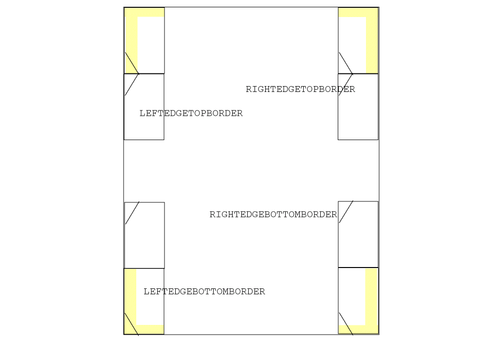
LEFTTOPEDGENEIGHBOR,RIGHTTOPEDGENEIGHBOR,LEFTBOTTOMEDGENEIGHBOR,RIGHTBOTTOMEDGENEIGHBOR, LEFTTOPCORNERNEIGHBOR, RIGHTTOPCORNERNEIGHBOR, LEFTBOTTOMCORNERNEIGHBORandRIGHTBOTTOMCORNERNEIGHBORFigure 1-36 Illustration of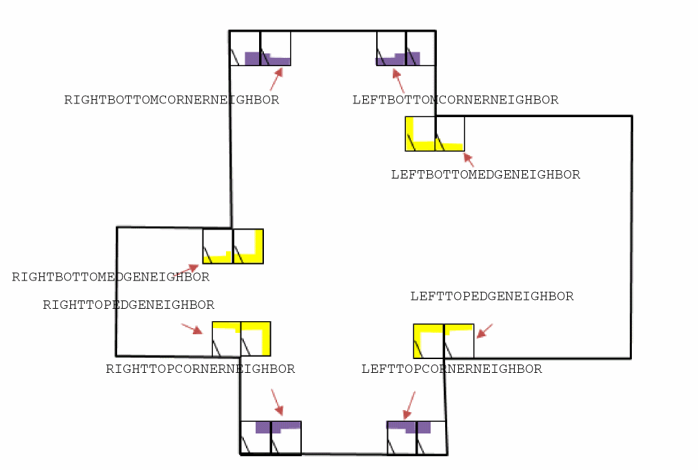
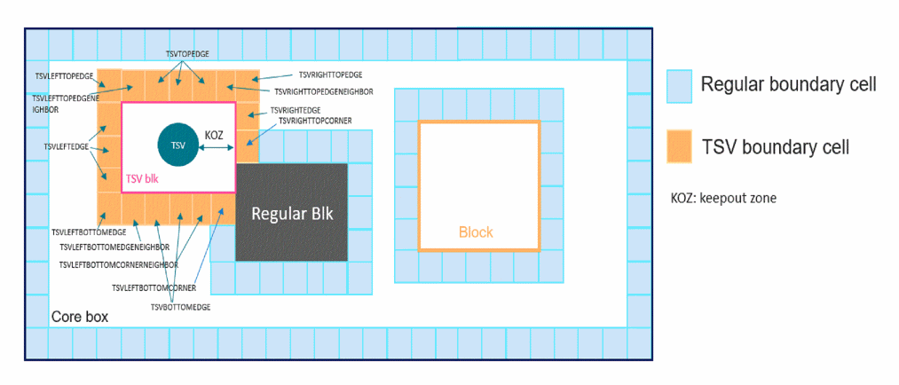
LEFTCORNERTOPBORDER,RIGHTCORNERTOPBORDER,LEFTCORNERBOTTOMBORDER,RIGHTCORNERBOTTOMBORDER,TOPCORNEREDGENEIGHBOR, andBOTTOMCORNEREDGENEIGHBORFigure 1-37 Illustration of TSV* End Cap Cells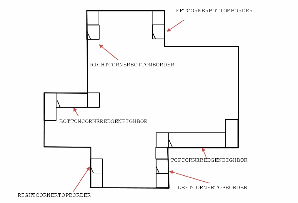
-
Constraint Area Type Rule
The constraint area type rule can be used to define a list of constraint rectangular areas.
You can create a constraint area type rule by using the following property definition:
PROPERTY LEF58_CONSTRAINTAREATYPE"“CONSTRAINTAREATYPEtypeName{RECTpt pt}... ;...” ;
Edge Type Rule
The edge type rule can be used to define edge types for right and left edges.
You can create an edge type rule by using the following property definition:
PROPERTY LEF58_EDGETYPE
"EDGETYPE {RIGHT | LEFT | TOP | BOTTOM}
    edgeType | BOTHSOURCE | SOURCEDRAIN | DRAINSOURCE | BOTHDRAIN
    | BOTHFLOATING
    [CELLROW cellRow  | HALFROW halfRow | RANGE xLow xHigh]
    ;..." ;
|
Defines which cell row, cellRow, the edgeType is defined on for multiple height cells, which can only be defined on |
||
|
|
||
|
Defines an edge type, edgeType, on the specified edge (
Edges of those special types may or may not have corresponding spacing defined in See Figure 1-39. |
||
|
Defines the edge type per half row, which can be defined only on the
Multiple height cells would have the same meaning and values of |
||
|
Defines a partial range of an edge that the type should be labeled. This can only be defined on |
||
You can define multiple EDGETYPE statements on an edge, including single height cells, such that different type of constraints can be defined on an edge.
-
The following statement indicates that edge type
GROUP1contains the right edge ofMACRO1andGROUP2contains the left edge ofMACRO1and right edge ofMACRO2:MACRO MACRO1
…
PROPERTY LEF58_EDGETYPE "
EDGETYPE RIGHT GROUP1 ;
EDGETYPE LEFT GROUP2 ; " ;
END MACRO1
MACRO MACRO2
…
PROPERTY LEF58_EDGETYPE "
EDGETYPE RIGHT GROUP2 ; " ;
END MACRO2
-
The following example indicates that
GROUP1andGROUP2are defined on the first and last (third) row, respectively, on the left edge for the triple-height cell:PROPERTY LEF58_EDGETYPE "
EDGETYPE LEFT GROUP1 CELLROW 1 ;
EDGETYPE LEFT GROUP2 CELLROW 3 ; " ;
Figure 1-38 Illustration of Macro with Cell Row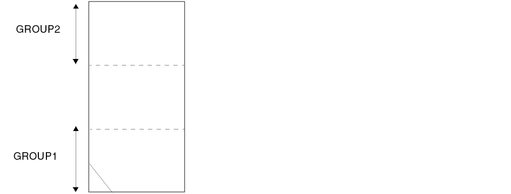
-
The following example indicates that
GROUP1andGROUP2are defined on the first and last (fourth) half row, respectively, on the right edge of the double-height cell:PROPERTY LEF58_EDGETYPE "
EDGETYPE RIGHT GROUP1 HALFROW 1 ;
EDGETYPE RIGHT GROUP2 HALFROW 4 ; " ;
Figure 1-39 Illustration of Macro with Half Row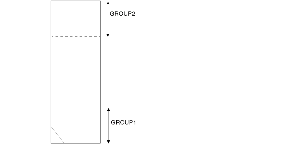
-
The following example illustrates the edge type rule with special edge type keywords:
MACRO A
...
PROPERTY LEF58_EDGETYPE
"EDGETYPE LEFT DRAINSOURCE ;
EDGETYPE RIGHT SOURCEDRAIN ; " ;
...
END A
MACRO B
...
PROPERTY LEF58_EDGETYPE "
EDGETYPE LEFT BOTHDRAIN ;
EDGETYPE RIGHT BOTHSOURCE ; " ;
...
END B
Figure 1-40 Illustration of Macro with special edge type keywordsFigure 1-41 Illustration of Macro with Range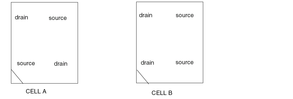
EEQ Rule
You can use the EEQ rule to specify the electrically equivalent (EEQ) variant for macros with class CORE standard cells.
You can create an EEQ rule by using the following property definition:
PROPERTY LEF58_EEQ
     "EEQ macroName [VARIANT num]
     ;... " ;
All other keywords are same as the existing macro EEQ syntax.
Foreign Rule
You can use the foreign rule to indicate that the foreign structure of the specified foreign orient should be used if a component of the macro matches one of the given component orientations.
You can create foreign rule by using the following property definition:
PROPERTY LEF58_FOREIGN
     "FOREIGN foreignCellName [pt [orient]]
          [COMPORIENT foreignOrientName {compOrient}...]...
     ;... " ;
All other keywords are same as the existing macro FOREIGN syntax.
The following example indicates that the foreign structure of foreign orient EFG should be applied if the instance is placed with orientation of S or FS, and all the other instances use the foreign orient ABC.
PROPERTY LEF58_FOREIGN
"FOREIGN ABC COMPORIENT EFG S FS ; " ;
Layer Mask Shift Rule
You can create a layer mask shift rule to specify that the mask could be shifted on the given layers.
You can define a layer mask shift rule by using the following property definition:
PROPERTY LEF58_LAYERMASKSHIFT "LAYERMASKSHIFTlayer1[layer2...] ;" ;
OBS Partial Rule
You can use the OBS partial rule to indicate a partially routing blockage.
You can create a OBS partial rule by using the following property definition:
PROPERTY LEF58_OBSPARTIAL
"OBSPARTIAL {LAYER layerName
WIDTH width SPACING spacing RECT pt pt}...
; " ;
MACRO A
...
PROPERTY LEF58_OBSPARTIAL
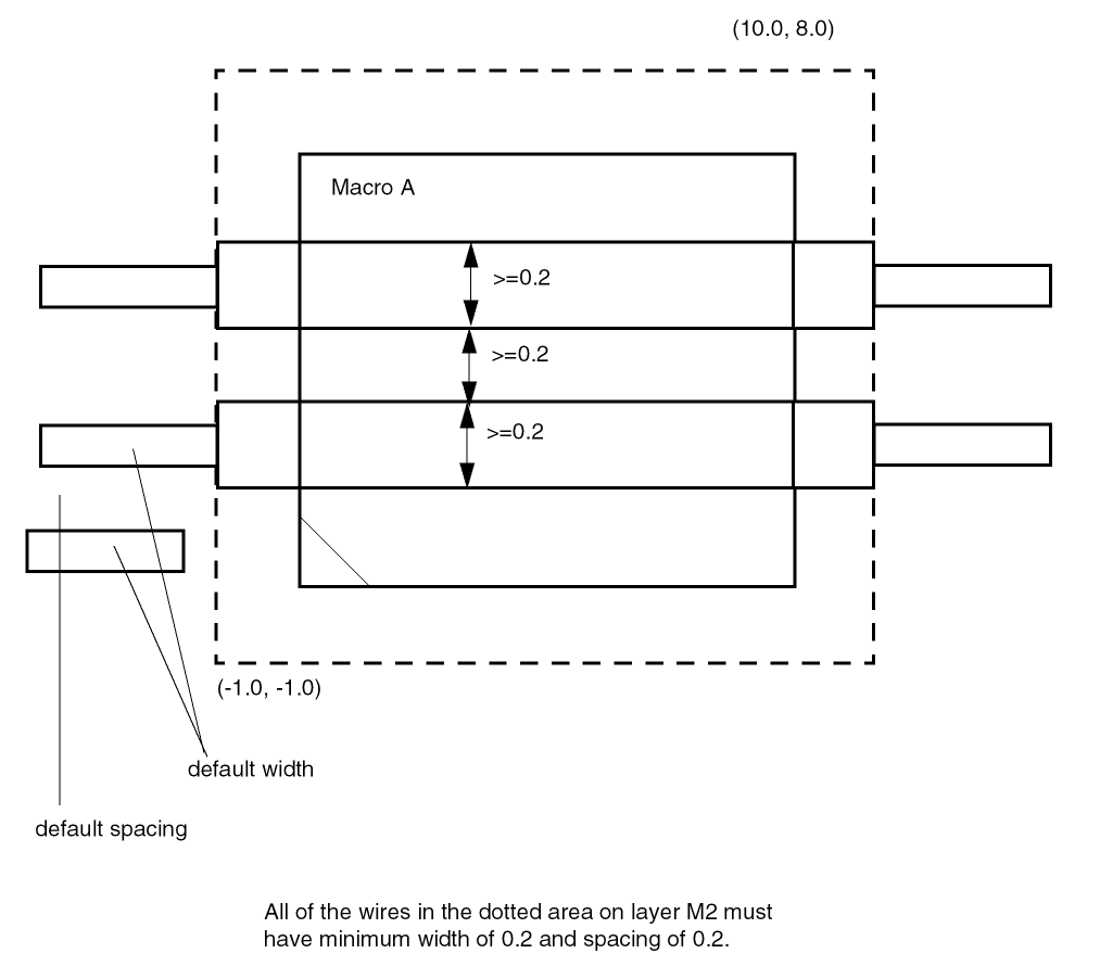
"OBSPARTIAL LAYER M2 WIDTH 0.2 SPACING 0.2
RECT -1.0 -1.0 10.0 8.0 ; " ;
Figure 1-42 Illustration of OBS Partial Rule
OBS Spacing Rule
You can use the OBS spacing rule to specify spacing for the OBS of the macro.
You can create a OBS spacing rule by using the following property definition:
PROPERTY LEF58_OBSSPACING
  "OBSSPACING {FULLDRC | MIN | spacing} [LAYER layer]...
  ; " ;
-
The following example indicates that all of the OBS on M3 would use 0.2 um while the rest of OBS uses min spacing.
PROPERTY LEF58_OBSSPACING “OBSSPACING MIN ;OBSSPACING 0.2 LAYER M3 ; ” ; -
The following example indicates that all of the OBS on M1 and M2 of this macro would use min spacing while M3 OBS would use 0.2um.
PROPERTY LEF58_OBSSPACING “OBSSPACING MIN LAYER M1 LAYER M2 ;OBSSPACING 0.2 LAYER M3 ;” ; -
The following example indicates that all of the OBS on M7 and M8 are real geometries that get full DRC checks, while the OBS on other layers are “abstract” blockages that only need min spacing checked.
PROPERTY LEF58_OBSSPACING “OBSSPACING MIN ;OBSSPACING FULLDRC LAYER M7 LAYER M8 ;” ;
Place Within Rule
You can use the OBS spacing rule to specify place within conditions for a filler cell.
You can create a place within rule by using the following property definition:
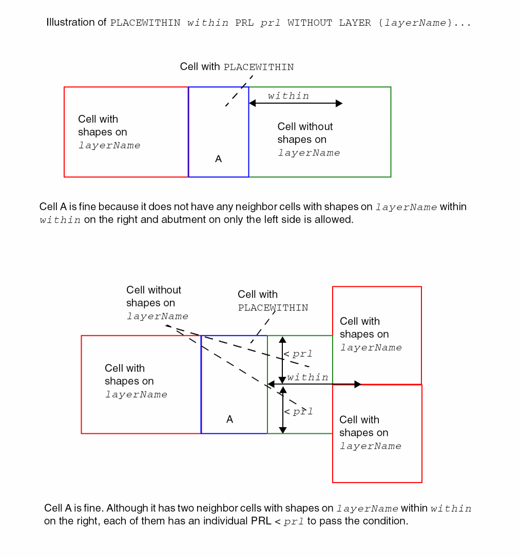
PROPERTY LEF58_PLACEWITHIN "PLACEWITHINwithinPRLprl{WITH|WITHOUT} LAYER {layerName}... ; " ;
Figure 1-43 Illustration of the Place Within Rule Using WITH
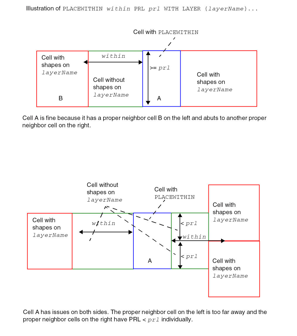
Figure 1-44 Illustration of the Place Within Rule Using WITHOUT
REQ Rule
You can define a REQ rule by using the following property definition:
PROPERTY LEF58_REQ
   "REQ macroName
    ; " ;
Tap Center Offset Rule
You can use the tap center offset rule to specify an offset value from the cell center from which the tap distance should be measured.
You can create a tap center offset rule by using the following property definition:
PROPERTY LEF58_TAPCENTEROFFSET
  "TAPCENTEROFFSET
    {offset | {HALFROW rowNum [LEFT|RIGHT] offset}...}
  ; " ;
Tap Center Offset Rule Example
MACRO A
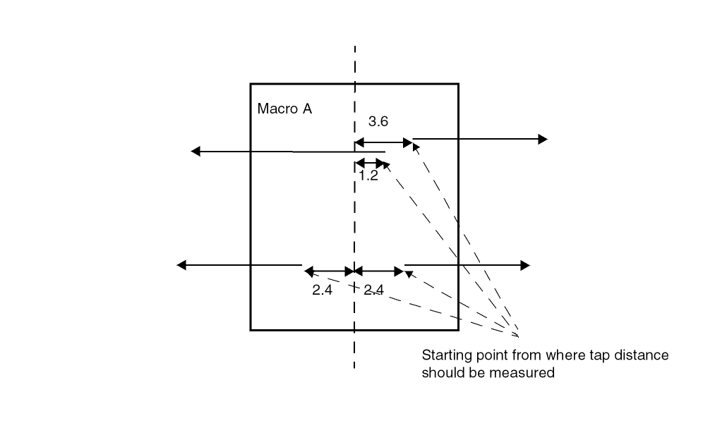
PROPERTY LEF58_TAPCENTEROFFSET “
TAPCENTEROFFSET HALFROW 1 2.4
HALFROW 2 LEFT -1.2 HALFROW 2 RIGHT 3.6 ; “ ;
...
END A
Figure 1-45 Illustration of Tap Center Offset Rule
Defining Cover Macros
If you define a cover macro with its actual size, some place-and-route tools cannot place the rest of the cells in your design because it uses the cell boundary to check for overlaps. You can resolve this in two ways:
- The easiest way to support a cover macro is to define the cover macro with a small size, for example, 1 by 1.
-
If you want to define the cover macro with its actual size, create an overlap layer with the non-routing
LAYERTYPEOVERLAPstatement. You define this overlap layer (cover macro) with the macro obstruction (OBS) statement.
Defining Symmetry
Symmetry statements specify legal orientations for sites and macros. Figure 1-45 illustrates the normal orientations for single-height, flipped and abutted rows with standard cells and sites.
Figure 1-46 Normal Orientations for Single-Height Rows
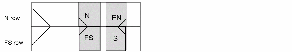
The following examples describe typical combinations of orientations for standard cells. Applications typically create only N (or FS for flipped) row orientations for horizontal standard cell rows; therefore, the examples describe these two rows.
Example 1-6 Single-Height Cells
Single-height cells for flipped and abutted rows should have SITE symmetry Y and MACRO symmetry X Y. These specifications allow N and FN macros in N rows, and FS and S macros in FS rows, see Figure 1-46. These symmetries work with flipped and abutted rows, as well as rows that are not flipped and abutted, so if the rows are all N orientation, the cells all have N or FN orientation. The extra MACRO symmetry of X is not required in this case, but causes no problems.
Figure 1-47 Legal Placements for Row Sites with Symmetry Y
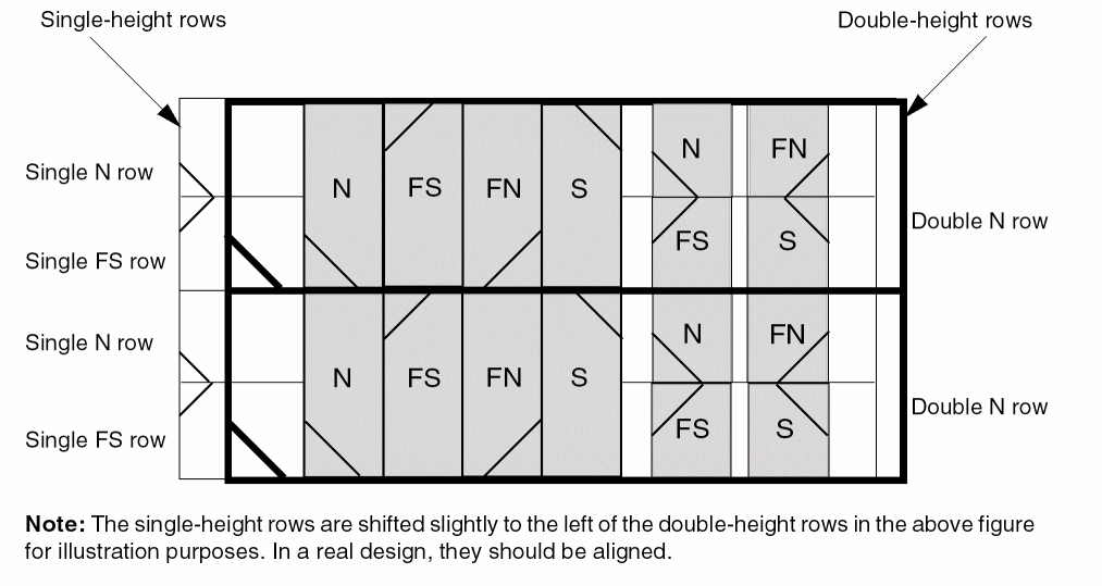
Example 1-7 Double-Height Cells
Double-height cells that are intended to align with flipped and abutted single-height rows should have SITE symmetry X Y and MACRO symmetry X Y. These symmetries allow all four cell orientations (N, FN, FS, and S) to fit inside the double-height row (see Figure 1-47). Usually, double-height rows are just N orientation rows that are abutted and aligned with a pair of single-height flipped and abutted rows.
Figure 1-48 Legal Placements for Single-Height Row Sites with Symmetry Y and Double-Height Row Sites with Symmetry X Y
Example 1-8 Special Orientations
Some single-height cells have special orientation needs. For example, the design requires flipped and abutted rows, but only N and FS orientations are allowed because of the special layout of well taps on the right side of a group of cells that borrow from the left side of the next cell. That is, you cannot place an N and FN cell against each other in one row because only N cells are allowed in an N row. In this case, the SITE symmetry should not be defined, and the MACRO symmetry should be X. A MACRO symmetry of X Y can also be defined because the Y-flipped macros (FN and S orientations) do not match the N or FS rows. See Figure 1-48 for the different combinations when the SITE has no symmetry.
Figure 1-49 Legal Placements for Row Sites with No Symmetry
Vertical rows use N or FN row and site orientations. The flipped, abutted vertical row orientation is N and FN, rather than the horizontal row orientation of N and FS. Otherwise, the meaning of the site symmetries and macro symmetries is the same as those for horizontal rows.
Single-height sites are normally given symmetry X, and single-height cells are normally given symmetry X Y. Example d in Figure 1-49 shows the legal placement for a site with symmetry X, and the typical standard cell MACRO symmetry X Y.
Figure 1-50 Legal Placements for Vertical Row Sites With Symmetry X
Layer Geometries
     { LAYER layerName
    [EXCEPTPGNET]
    [SPACING minSpacing | DESIGNRULEWIDTH value] ;
  [WIDTH width ;]
  { PATH [MASK maskNum] pt ... ;
  | PATH [MASK maskNum] ITERATE pt ... stepPattern ;
  | RECT [MASK maskNum] pt pt ;
  | RECT [MASK maskNum] ITERATE pt pt stepPattern ;
  | POLYGON [MASK maskNum] pt pt pt pt ... ;
  | POLYGON [MASK maskNum] ITERATE pt pt pt pt ... stepPattern ;
  } ...
| VIA [MASK viaMaskNum] pt viaName ;
| VIA ITERATE [MASK viaMaskNum] pt viaName stepPattern ;
} ...
Used in the macro obstruction (OBS) and pin port (PIN) statements to define layer geometries in the design.
|
Specifies the effective design rule width. If specified, the obstruction or pin is treated as a shape of this width for all spacing checks. If you specify |
||
|
Indicates that the obstruction shapes block signal routing, but do not block power or ground routing. This can be used to block signal routes that might cause noise, but allow connections to power and ground pins. |
||
|
Creates an array of the |
||
|
Specifies the spacing, in distance units, between the columns and rows of points. |
||
|
Specifies the layer on which to place the geometry. Note: For macro obstructions, you can specify cut, implant, or overlap layers. |
||
|
Specifies which mask from double- or triple-patterning to use for this shape. The maskNum variable must be a positive integer. Most applications only support values of 1, 2, or 3.
Shapes without any defined mask have no mask set (they are considered uncolored). The uncolored PIN shapes can be assigned to an arbitrary mask as long as they do not have a spacing conflict with neighbor objects. The meaning of uncolored OBS shapes depends on the cell. For standard cell MACROs (with a |
||
|
Specifies which mask for double- or triple-patterning lithography to be applied to via shapes on each layer. The viaMaskNum is a hex-encoded 3 digit value of the form: <
For example, MASK 113 means the top metal and cut layer maskNum is |
||
|
The topMaskNum and bottomMaskNum variables specify which mask the corresponding metal shape belongs to. The via-master metal mask values have no effect. For the cut-layer, the cutMaskNum defines the mask for the bottommost, and then the leftmost cut. For multi-cut vias, the via-instance cut masks are derived from the via-master cut mask values. The via-master must have a mask defined for all of the cut shapes and every via-master cut mask is "shifted" (1 to 2, 2 to 1 for two mask layers, and 1 to 2, 2 to 3, 3 to 1 for three mask layers) so the lower-left cut matches the cutMaskNum value. See Example 1-11 . Similarly, for the metal layer, the topMaskNum/bottomMaskNum would define the mask for the bottom-most, then leftmost metal shape. For multiple disjoint metal shapes, the via-instance metal masks are derived from the via-master metal mask values. The via-master must have a mask defined for all of the metal shapes, and every via-master metal mask is “shifted” (1->2, 2->1 for two mask layers, 1->2, 2->3, 3->1 for three mask layers) so the lower-left cut matches the topMaskNum/bottomMaskNum value. Shapes without any defined mask that need to be assigned, can be assigned to an arbitrary choice of mask by applications. |
||
|
Creates a path between the specified points, such as pt1 pt2 pt3. The path automatically extends the length by half of the current width on both endpoints to form a rectangle. (A previous You can also specify a path with a single coordinate, in which case a square whose side is equal to the current width is placed with its center at pt. |
||
|
Specifies a sequence of at least three points to generate a polygon geometry. Most fab DRC rules require each polygon edge to be parallel to the x or y axis, or at a 45-degree angle. However, odd-angles are allowed sometimes on a few layers, such as bump layers. Each |
||
|
Specifies a rectangle, where the two points specified are opposite corners of the rectangle. There is no functional difference between a geometry specified using |
||
|
Specifies the minimum spacing allowed between this particular
One common application is to put an
The minSpacing value cannot be larger than the maximum spacing defined in the |
||
|
Specifies the width that the |
||
The following example shows how to define a set of geometries, first by using ITERATE statements, then by using individual PATH, VIA and RECT statements.
The following two sets of statements are equivalent:
PATH ITERATE 532.0 534 1999.2 534
DO 1 BY 2 STEP 0 1446 ;
VIA ITERATE 470.4 475 VIABIGPOWER12
DO 2 BY 2 STEP 1590.4 1565 ;
RECT ITERATE 24.1 1.5 43.5 16.5
DO 2 BY 1 STEP 20.0 0 ;
PATH 532.0 534 1999.2 534 ;
PATH 532.0 1980 1999.2 1980 ;
VIA 470.4 475 VIABIGPOWER12 ;
VIA 2060.8 475 VIABIGPOWER12;
VIA 470.4 2040 VIABIGPOWER12;
VIA 2060.8 2040 VIABIGPOWER12;
RECT 24.1 1.5 43.5 16.5 ;
RECT 44.1 1.5 63.5 16.5 ;
Example 1-11 Layer Geometries - multi-mask patterns
The following example shows how to use multi-mask patterns:
LAYER M1 ;
RECT MASK 2 10 10 11 11 ;
LAYER M2 ;
RECT 10 10 11 11 ;
VIA 5 5 VIA1_1 ;
VIA MASK 031 15 15 VIA1_2 ;
-
M1rect shape belongs toMASK 2 -
M2rect shape has no mask set -
VIA1_1via has no mask set (all the metal and cut shapes have no mask) -
VIA1_2via will have:- No mask set for the top metal shape (topMaskNum is 0 in the 031 value)
-
MASK 1for the bottom metal shape (botMaskNum is 1 in the 031 value) -
The bottommost, and then the leftmost cut of the via-instance is
MASK 3. The mask for the other cuts of the via-instance are derived from the via-master by "shifting" the via-master cut masks to match. So if the via-master's bottom-left cut isMASK 1, then the via-master cuts onMASK 1becomeMASK 3for the via-instance, and similarly cuts on 2 to 1, and cuts on 3 to 2. See Figure 1-50.
LAYER M1 ;
RECT MASK 2 10 10 11 11 ;
LAYER M2 ;
RECT 10 10 11 11 ;
VIA 5 5 VIA1_1 ;
VIA MASK 031 15 15 VIA1_2 ;
Figure 1-51 Via-master multi-mask patterns
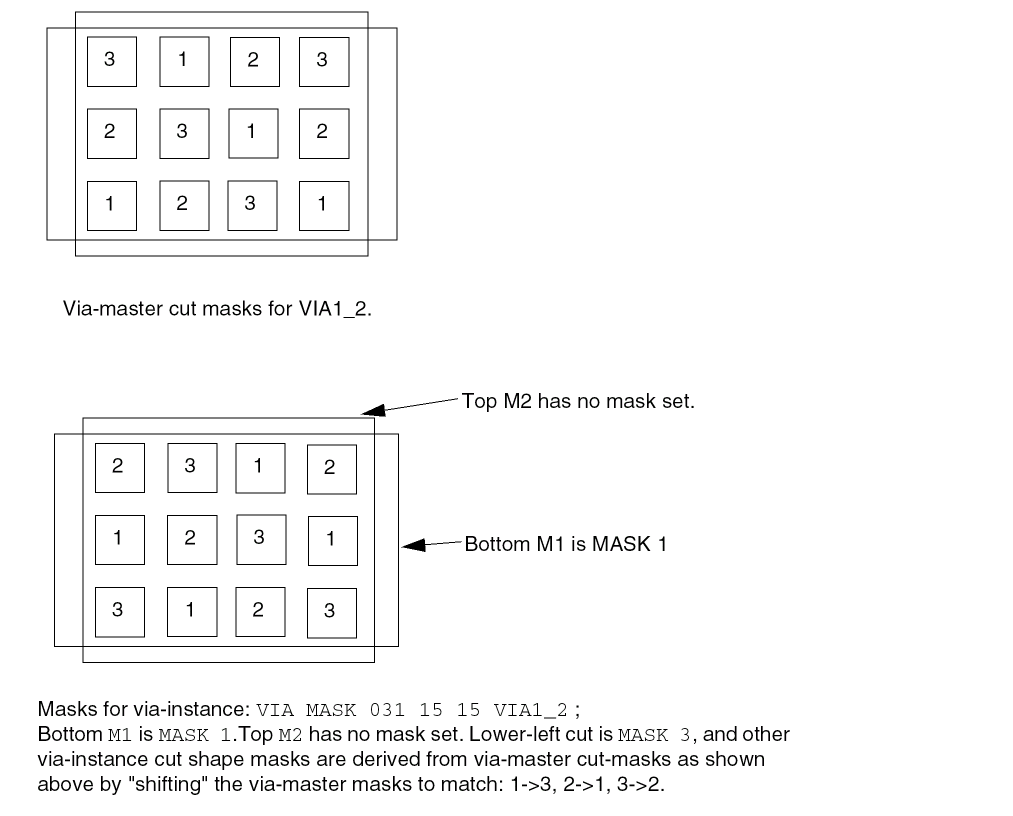
Macro Obstruction Statement
[OBS
{layerGeometries}...
END]
Defines a set of obstructions (also called blockages) on the macro. You specify obstruction geometries using the layer geometry syntax. See “Layer Geometries” for syntax information.
Normally, obstructions block routing, except for when a pin port overlaps an obstruction (a port geometry overrules an obstruction). For example, you can define a large rectangle for a metal1 obstruction and have metal1 port in the middle of the obstruction. The port can still be accessed by a via, if the via is entirely inside the port.
In Figure 1-51, the router can only access the metal1 port from the right. If the metal2 obstruction did not exist, the router could connect to the port with a metal12 via, as long as the metal1 part of the via fit entirely inside the metal1 port.
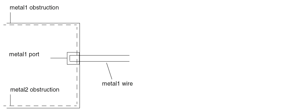
Routing can also connect to such a port on the same layer if the routing does not cross any obstruction by more than a distance of the total of minimum width plus minimum spacing before reaching the pin. This is because the port geometry is known to be “real,” and any obstruction less than a distance of minimum width plus minimum spacing away from the port is not a real obstruction. If the pin is more than minimum width plus minimum spacing away from the obstruction edge, the router can only route to the pin from the layer above or below using a via (see Figure 1-52).
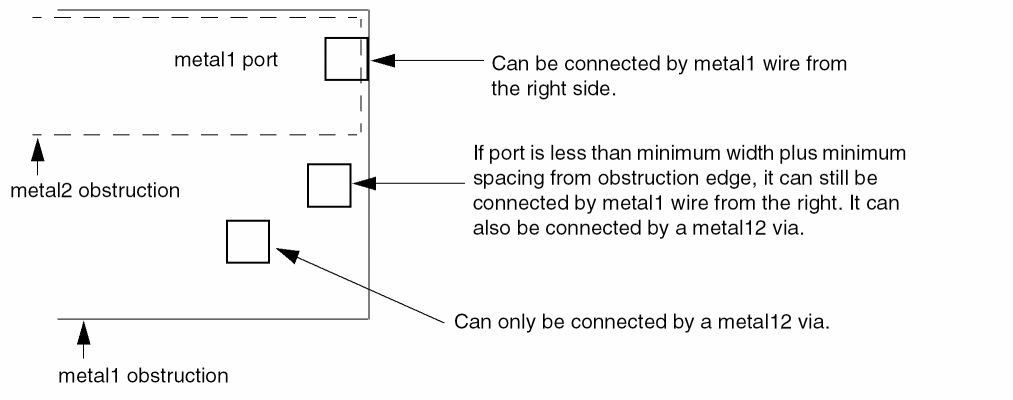
If a port is on the edge of the obstruction, a wire can be routed to the port without violations. Pins that are partially covered with obstructions or in apparent violation with nearby obstructions can limit routing options. Even though the violations are not real, the router assumes they are. In these cases, extend each obstruction to cover the pin. The router then accesses the pin as described above.
Benefits of Combining Obstructions
Significant routing time can be saved if obstructions are simplified. Especially in metal1, construct obstructions so that free tracks on the layer are accessible to the router. If most of the routing resource is obstructed, simplify the obstruction modeling by combining small obstructions into a single large obstruction. For example, use the bounding box of all metal1 objects in the cell, rather than many small obstructions, as the bounding box of the obstruction.
You must be sure to model via obstructions over the rest of the cell properly. A single, large cut12 obstruction over the rest of the cell can do this in some cases, as when metal1 resource exists within the cell outside the power buses.
Rectilinear Blocks
Normally, footprint descriptions in LEF are rectangular. However, it is possible to describe rectilinear footprints using an overlap layer. The overlap layer is defined specifically for this purpose and does not contain any routing.
Describe a rectilinear footprint by setting the SIZE of the macro as a whole to a rectangular bounding box, then defining obstructions within the bounding box on the overlap layer. The obstructions on the overlap layer indicate areas within the bounding box which no other macro should overlap. The obstructions should completely cover the rectilinear shape of the macro, but not the portion of the bounding box that might overlap with other macros during placement.
OBS statement. To do this, specify a layer of type OVERLAP and then give the overlap geometries, as shown in Figure 1-53.
Macro Pin Statement
[PIN pinName [TAPERRULEruleName;] [DIRECTION {INPUT | OUTPUT [TRISTATE] | INOUT | FEEDTHRU} ;] [USE { SIGNAL | ANALOG | POWER | GROUND | CLOCK } ;] [NETEXPR "netExprPropNamedefaultNetName" ;] [SUPPLYSENSITIVITYpowerPinName;] [GROUNDSENSITIVITYgroundPinName;] [SHAPE {ABUTMENT | RING | FEEDTHRU} ;] [MUSTJOINpinName;] {PORT[CLASS {NONE | CORE | BUMP} ;] {layerGeometries} ... END} ... [PROPERTYpropName propVal;] ... [PROPERTY LEF58_ACCESSAREA "ACCESSAREA {LAYERlayerNameRECTpt pt[CUTCLASSclassName] [EXCEPTEXTRACUT]}... ; " ;] [PROPERTY LEF58_ANTENNADIFFAREA "ANTENNADIFFAREA [BACKSIDE][PROTECTOR]value[LAYERlayerName] ; ..." ;] [PROPERTY LEF58_MUSTJOINALLPORTS "MUSTJOINALLPORTS ; " ;] [PROPERTY LEF58_VIAINMUSTJOIN "VIAINMUSTJOIN ; " ;] [PROPERTY LEF58_VIAINPINONLY "VIAINPINONLY ; " ;] [ANTENNAPARTIALMETALAREAvalue[LAYERlayerName] ;] ... [ANTENNAPARTIALMETALSIDEAREAvalue[LAYERlayerName] ;] ... [ANTENNAPARTIALCUTAREAvalue[LAYERlayerName] ;] ... [ANTENNADIFFAREAvalue[LAYERlayerName] ;] ... [ANTENNAMODEL {OXIDE1 | OXIDE2 | OXIDE3 | OXIDE4} ;] ... [ANTENNAGATEAREAvalue[LAYERlayerName] ;] ... [ANTENNAMAXAREACARvalueLAYERlayerName;] ... [ANTENNAMAXSIDEAREACARvalueLAYERlayerName;] ... [ANTENNAMAXCUTCARvalueLAYERlayerName;] ...
END pinName]
Defines pins for the macro. PIN statements must be included in the LEF specification for each macro. All pins, including VDD and VSS, must be specified. The first pin listed becomes the first pin in the database. List the pins in the following order:
ANTENNADIFFAREA value [LAYER layerName]
Specifies the diffusion (diode) area, in micron-squared units, to which the pin is connected on a layer. If you do not specify a layer name, the value applies to all layers. For more information on process antenna calculation, see Appendix C, “Calculating and Fixing Process Antenna Violations.”
ANTENNAGATEAREA value [LAYER layerName]
Specifies the gate area, in micron-squared units, to which the pin is connected on a layer. If you do not specify a layer name, the value applies to all layers. For more information on process antenna calculation, see Appendix C, “Calculating and Fixing Process Antenna Violations.”
ANTENNAMAXAREACAR value LAYER layerName
For hierarchical process antenna effect calculation, specifies the maximum cumulative area ratio value on the specified layerName, using the metal area at or below the current pin layer, excluding the pin area itself. This is used to calculate the actual cumulative antenna ratio on the pin layer, or the layer above it.
For more information on process antenna calculation, see Appendix C, “Calculating and Fixing Process Antenna Violations.”
ANTENNAMAXCUTCAR value LAYER layerName
For hierarchical process antenna effect calculation, specifies the maximum cumulative antenna ratio value on the specified layerName, using the cut area at or below the current pin layer, excluding the pin area itself. This is used to calculate the actual cumulative antenna ratio for the cuts above the pin layer.
For more information on process antenna calculation, see Appendix C, “Calculating and Fixing Process Antenna Violations.”
ANTENNAMAXSIDEAREACAR value LAYER layerName
For hierarchical process antenna effect calculation, specifies the maximum cumulative antenna ratio value on the specified layerName, using the metal side wall area at or below the current pin layer, excluding the pin area itself. This is used to calculate the actual cumulative antenna ratio on the pin layer or the layer above it.
For more information on process antenna calculation, see Appendix C, “Calculating and Fixing Process Antenna Violations.”
ANTENNAMODEL {OXIDE1 | OXIDE2 | OXIDE3 | OXIDE4}
Specifies the oxide model for the pin. If you specify an ANTENNAMODEL statement, the value affects all ANTENNAGATEAREA and ANTENNA*CAR statements for the pin that follow it until you specify another ANTENNAMODEL statement. The ANTENNAMODEL statement does not affect ANTENNAPARTIAL*AREA and ANTENNADIFFAREA statements because they refer to the total metal, cut, or diffusion area connected to the pin, and do not vary with each oxide model.
Default: OXIDE1, for a new PIN statement
Because LEF is often used incrementally, if an ANTENNA statement occurs twice for the same oxide model, the last value specified is used.
For most standard cells, there is only one value for the ANTENNAPARTIAL*AREA and ANTENNADIFFAREA values per pin; however, for a block with six routing layers, it is possible to have six different ANTENNAPARTIAL*AREA values and six different ANTENNAPINDIFFAREA values per pin. It is also possible to have six different ANTENNAPINGATEAREA and ANTENNAPINMAX*CAR values for each oxide model on each pin.
Example 1-12 Pin Antenna Model
The following example describes oxide model information for pins IN1 and IN2.
MACRO GATE1
PIN IN1
ANTENNADIFFAREA 1.0 ; #not affected by ANTENNAMODEL
...
ANTENNAMODEL OXIDE1 ; #OXIDE1 not required, but is good
#practice
ANTENNAGATEAREA 1.0 ; #OXIDE1 gate area
ANTENNAMAXAREACAR 50.0 LAYER m1 ; #metal1 CAR value
...
ANTENNAMODEL OXIDE2 ; #OXIDE2 starts here
ANTENNAGATEAREA 3.0 ; #OXIDE2 gate area
...
PIN IN2
ANTENNADIFFAREA 2.0 ; #not affected by ANTENNAMODEL
ANTENNAPARTIALMETALAREA 2.0 LAYER m1 ;
...
#no OXIDE1 specified for this pin
ANTENNAMODEL OXIDE2 ;
ANTENNAGATEAREA 1.0 ;
...
ANTENNAPARTIALCUTAREA value [LAYER layerName]
Specifies the partial cut area above the current pin layer and inside the macro cell on the layer. For a hierarchical design, only the cut layer above the I/O pin layer is needed for partial antenna ratio calculation. If you do not specify a layer name, the value applies to all layers.
For more information on process antenna calculation, see Appendix C, “Calculating and Fixing Process Antenna Violations.”
ANTENNAPARTIALMETALAREA value [LAYER layerName]
Specifies the partial metal area connected directly to the I/O pin and the inside of the macro cell on the layer. For a hierarchical design, only the same metal layer as the I/O pin, or the layer above it, is needed for partial antenna ratio calculation. If you do not specify a layer name, the value applies to all layers.
For more information on process antenna calculation, see Appendix C, “Calculating and Fixing Process Antenna Violations.”
Note: Metal area is calculated by adding the pin’s geometric metal area and the ANTENNAPARTIALMETALAREA value.
ANTENNAPARTIALMETALSIDEAREA value [LAYER layerName]
Specifies the partial metal side wall area connected directly to the I/O pin and the inside of the macro cell on the layer. For a hierarchical design, only the same metal layer as the I/O pin or the layer above is needed for partial antenna ratio calculation. If you do not specify a layer name, the value applies to all layers.
For more information on process antenna calculation, see Appendix C, “Calculating and Fixing Process Antenna Violations.”
DIRECTION {INPUT | OUTPUT [TRISTATE] | INOUT | FEEDTHRU}Specifies the pin type. Most current tools do not usually use this keyword. Typically, pin directions are defined by timing library data, and not from LEF.
Default: INPUT
Value: Specify one of the following:
|
Pin that drives signals out of the cell. The optional |
|
|
Pin that can accept signals going either in or out of the cell. |
|
GROUNDSENSITIVITY groundPinName
Specifies that if this pin is connected to a tie-low connection (such as 1’b0 in Verilog), it should connect to the same net to which groundPinName is connected.
groundPinName must match a pin on this macro that has a USE GROUND attribute. The ground pin definition can follow later in this MACRO statement; it does not have to be defined before this pin definition. For an example, see Example 1-13.
Note: GROUNDSENSITIVITY is useful only when there is more than one ground pin in the macro. By default, if there is only one USE GROUND pin, then the tie-low connections are already implicitly defined (that is, tie-low connections are connected to the same net as the one ground pin).
Specifies the name of another pin in the cell that must be connected with the pin being defined. MUSTJOIN pins provide connectivity that must be made by the router. In the LEF file, each pin referred to must be defined before the referring pin. The remaining MUSTJOIN pins in the set do not need to be defined contiguously.
Note: MUSTJOIN pin names are never written to the DEF file; they are only used by routers to add extra connection points during routing.
MUSTJOIN pins have the following restrictions:
Schematic and nonschematic MUSTJOIN pins are handled in slightly different ways. For schematic MUSTJOIN pins, the pins are added to the pin set for the (unique) net associated with the ring for each component instance of the macro. The net is routed in the usual manner, and routing data for the MUSTJOIN pins are included in routing data for the net.
The mustjoin routing is not necessarily performed before the rest of the net. Timing relations should not be given for MUSTJOIN pins, and internal mustjoin routing is modeled as lumped capacitance at the schematic pin.
Nonschematic MUSTJOIN pin sets get routed in the usual manner. However, when the DEF file is outputted, routing data is reported in the NETS section of the file as follows:
MUSTJOINcompNamepinName+regularWiring;
Here, compName is the component and pinName is an arbitrary pin in the set. You can also use the preceding to input prewiring for the MUSTJOIN pin, using FIXED or COVER.
NETEXPR "netExprPropName defaultNetName"
Specifies a net expression property name (such as power1 or power2) and a default net name. If netExprPropName matches a net expression property in the netlist (such as in Verilog, VHDL, or OpenAccess), then the property is evaluated, and the software identifies a net to which to connect this pin. If this property does not exist, defaultNetName is used for the net name.
netExprPropName must be a simple identifier in order to be compatible with other languages, such as Verilog and CDL. Therefore, it can only contain alphanumeric characters, and the first character cannot be a number. For example, power2 is a legal name, but 2power is not. You cannot use characters such as $ and !. The defaultName can be any legal DEF net name.
Example 1-13 Net Expression and Supply Sensitivity
The following statement defines sensitivity and net expression values for four pins on the macro myMac:
MACRO myMac
...
PIN in1
...
SUPPLYSENSITIVITY vddpin1 ; #If in1 is 1’b1, use net connected to vddpin1.
                           #Note that no GROUNDSENSITIVITY is needed
                           #because only one ground pin exists.
                           #Therefore, 1’b0 implicitly means net from
                           #pin gndpin.
...
END in1
PIN vddpin1
...
NETEXPR "power1 VDD1" ; #If power1 net expression is defined in the
                        #netlist, use it to find the net connection. If
                        #not, use net VDD1.
...
END vddpin1
PIN vddpin2
...
NETEXPR "power2 VDD2" ; #If power2 net expression is defined in the
                        #netlist, use it to find the net connection.If
                        #not, use net VDD2.
...
END vddpin2
PIN gndpin
...
NETEXPR "gnd1 GND" ; #If gnd1 net expression is defined in the
                     #netlist, use  it to find the net connection. If
                     #not, use net GND.
...
END gndpin
...
END myMac
Specifies the name for the library pin.
Starts a pin port statement that defines a collection of geometries that are electrically equivalent points (strongly connected). A pin can have multiple ports. Each PORT of the same PIN is considered weakly connected to the other PORTs, and should already be connected inside the MACRO (often through a resistive path).
Strongly connected shapes (that is, multiple shapes of one PORT) indicate that a signal router is allowed to connect to one shape of the PORT, and continue routing from another shape of the same PORT.
Weakly connected shapes (that is, separate PORTs of the same PIN) are assumed to be connected through resistive paths inside the MACRO that should not be used by routers. The signal router should connect to one or the other PORT, but not both.
Power routers should connect to every PORT statement, if there is more than one for a given PIN. For example, if a block has several PORTs on the boundary for the VSS PIN, each PORT should be connected by the power router.
The syntax for describing pin port statements is defined as follows:
{PORT
[CLASS {NONE | CORE | BUMP} ;]
{layerGeometries} ...
END} ...
|
Specifies the port type. A port can be one of the following:
|
|
|
Defines port geometries for the pin. You specify port geometries using layer geometries syntax. See “Layer Geometries” for syntax information. |
|
Specifies a numerical or string value for a pin property defined in the PROPERTYDEFINITIONS statement. The propName you specify must match the propName listed in the PROPERTYDEFINITIONS statement.
Specifies a pin with special connection requirements because of its shape.
Value: Specify one of the following:
|
Pin that goes straight through cells with a regular shape and connects to pins on adjoining cells without routing. |
|
|
Pin on a large block that forms a ring around the block to allow connection to any point on the ring. Cover macro special pins also typically have shape |
|
|
Pin with an irregular shape with a jog or neck within the cell. |
|
|
Figure 1-54 shows an example of an abutment and a feedthrough pin.
When you define feedthrough and abutment pins for use with power routing, you must do the following:
|
|
SUPPLYSENSITIVITY powerPinName
Specifies that if this pin is connected to a tie-high connection (such as 1’b1 in Verilog), it should connect to the same net to which powerPinName is connected.
powerPinName must match a pin on this macro that has a USE POWER attribute. The power pin definition can follow later in this MACRO statement; it does not have to be defined before this pin definition. For an example, see Example 1-13.
Note: SUPPLYSENSITIVITY is useful only when there is more than one power pin in the macro. By default, if there is only one USE POWER pin, then the tie-high connections are already implicitly defined (that is, tie-high connections are connected to the same net as the one power pin).
Specifies the nondefault rule to use when tapering wires to the pin.
USE {ANALOG | CLOCK | GROUND | POWER | SIGNAL}
Specifies how the pin is used. Pin use is required for timing analysis.
Default: SIGNAL
Value: Specify one of the following:
|
Pin is used for connectivity to the chip-level ground distribution network. |
|
|
Pin is used for connectivity to the chip-level power distribution network. |
|
Access Area Rule
The access area rule can be used to specify a via access area on the specified cut layer.
You can specify the access area rule by using the following property definition:
PROPERTY LEF58_ACCESSAREA"ACCESSAREA {LAYERlayerNameRECTpt pt[CUTCLASSclassName] [EXCEPTEXTRACUT]}... ; " ;
-
The diagram below illustrates a case where the access area rule is defined for the pin as well as macro:
MACRO Z
...
PROPERTY LEF58_ACCESSAREA "
ACCESSAREA LAYER VIA1 RECT 3.0 2.2 5.5 3.0 ; " ;
PIN A
...
PROPERTY LEF58_ACCESSAREA "
ACCESSAREA LAYER VIA1 RECT 1.0 1.0 3.5 1.8 ; " ;
...
END A
...
END Z
Figure 1-56 Illustration of the Access Area Rule on a Pin
Antenna Diff Area Rule
The antenna diff area rule can be used to specify the diffusion area to which the pin is connected on a layer.
You can specify the antenna diff area rule by using the following property definition:
PROPERTY LEF58_ANTENNADIFFAREA"ANTENNADIFFAREA [BACKSIDE][PROTECTOR]value[LAYERlayerName] ; ..." ;
Must Join All Ports Rule
You can use the must join all ports rule to specify that all ports must be connected individually.
You can create a must join all ports rule by using the following property definition:
PROPERTY LEF58_MUSTJOINALLPORTS
“MUSTJOINALLPORTS
; “ ;
Specifies that all of the ports must be connected individually. If there are multiple shapes per ports, at least one of the shapes of the port needs to be connected. However, tools typically would connect to only one of the shapes.
PROPERTY LEF58_MUSTJOINALLPORTS “
means that the router must connect to at least one of the two M1 shapes and to the M2 shape individually. However, tools typically would connect to exactly one of the two M1 shapes and to the M2 shape individually.
Via In Must Join Rule
You can create a via in must join rule by using the following property definition:
PROPERTY LEF58_VIAINMUSTJOIN
“VIAINMUSTJOIN
; “ ;
Specifies that two stacked vias must be used to connect to the must-join pins and all of the cuts of these two stacked vias must be within the boundary box of the must-join pins. For example, if the must-join pins have multiple M1 shapes, the cuts of the stacked vias to M3 must be within the boundary box formed by the M1 pin shapes.
Via In Pin Only Rule
You can use the via in pin only rule to specify that vias must be dropped inside the original pin shapes to connect to the pin.
You can create a via in pin only rule by using the following property definition:
PROPERTY LEF58_VIAINPINONLY
“VIAINPINONLY
; ” ;
Specifies that at least one cut of a via must be dropped inside the original pin shapes to connect to the pin, and a planar connection to the pin is not allowed. In some advanced nodes, the pin shapes can be extended for metal alignment purpose. For a single-cut via, it means that the cut would be in the original pin shapes. For a multiple-cut via, particularly with the via pillar having multiple fingers, only one cut needs to be in the original pin shapes and the rest of the via pillar structure can be outside the original pin shapes.
To support negative enclosure, for a square cut with size CS greater than the minimum width W on the below or above metal layer of a pin shape, the following method is used to determine whether the cut is inside the pin shape. From the cut center, extend CS/2 on any two opposite sides and W/2 on the other two opposite sides, if one of the two expanded sizes (one for extending CS/2 horizontally and another for extending CS/2 vertically) is completely covered by the pin metal shape, the cut is considered to be inside the pin shape.
Manufacturing Grid
[MANUFACTURINGGRID value ;]
Defines the manufacturing grid for the design. The manufacturing grid is used for geometry alignment. When specified, shapes and cells are placed in locations that snap to the manufacturing grid.
Specifies the value for the manufacturing grid, in microns. value must be a positive number.
Type: Float
Maximum Via Stack
[MAXVIASTACKvalue[RANGEbottomLayertopLayer] ;]
Specifies the maximum number of single-cut stacked vias that are allowed on top of each other (that is, in one continuous stack). A via is considered to be in a stack with another via if the cut of the first via overlaps any part of the cut of the second via. A double-cut or larger via interrupts the stack. For example, a via stack consisting of single via12, single via23, double-cut via34, and single via45 has a single-cut stack of height 2 for via12 and via23, and a single-cut stack of height 1 for via45 because the full stack is broken up by double-cut via34.
The MAXVIASTACK statement should follow the LAYER statements in the LEF file; however, it is not attached to any particular layer. You can specify only one MAXVIASTACK statement in a LEF file.
Specifies a range of layers for which the maximum stacked via rule applies. If you do not specify a range, the value applies for all layers.
Specifies the maximum allowed number of single-cut stacked vias.
Type: Integer
Example 1-14 Maximum Via Stack Statement
The following MAXVIASTACK statement specifies that only four stacked vias are allowed on top of each other. This rule applies to all layers.
LAYER metal9
...
END LAYER
MAXVIASTACK 4 ;
If you specify the following statement instead, the stacked via limit applies only to layers metal1 through metal7.
MAXVIASTACK 4 RANGE m1 m7 ;
Nondefault Rule
[NONDEFAULTRULEruleName[HARDSPACING ;]{LAYERlayerNameWIDTHwidth; [DIAGWIDTHdiagWidth;][SPACINGminSpacing;] [WIREEXTENSIONvalue;] ENDlayerName} ... [VIAviaStatement] ... [USEVIAviaName;] ... [USEVIARULEviaRuleName;] ... [MINCUTScutLayerNamenumCuts;] ... [PROPERTYpropNamepropValue;] ... [PROPERTY LEF58_USEVIACUTCLASS “USEVIACUTCLASScutLayerName className[ROWCOLnumCutRows numCutCols] ;... “ ;]
END ruleName]
Defines the wiring width, design rule spacing, and via size for regular (signal) nets. You do not need to define cut layers for the non-default rule.
Some tools have limits on the total number of non-default rules they can store. This limit can be as low as 30; however most tools that support 90 nanometer rules (that is, LEF 5.5 and newer) can handle at least 255.
Specifies the diagonal width for layerName, when 45-degree routing is used.
Default: The minimum width value (WIDTH minWidth)
Type: Float, specified in microns
Specifies that any spacing values that exceed the LEF LAYER spacing requirements are “hard” rules instead of “soft” rules. By default, routers treat extra spacing requirements as soft rules that are high cost to violate, but not real spacing violations. However, in certain situations, the extra spacing should be treated as a hard, or real, spacing violation, such as when the route will be modified with a post-process that replaces some of the extra space with metal.
LAYER layerName ... END layerName
Specifies the layer for the various width and spacing values. This layer must be a routing layer. Every routing layer must have a WIDTH keyword and value specified. All other keywords are optional.
Specifies the minimum number of cuts allowed for any via using the specified cut layer. Routers should only use vias (generated or predefined fixed vias) that have at least numCuts cuts in the via.
Type: (numCuts) Positive integer
Specifies a name for the new routing rule. The name DEFAULT is reserved for the default routing rule used by most nets. The default routing rule is constructed automatically from the LEF LAYER statement WIDTH, DIAGWIDTH, SPACING, and WIREEXTENSION values, from the LEF VIA statement (any vias with the DEFAULT keyword), and from the LEF VIARULE statement (any via rules with the DEFAULT keyword). If you specify DEFAULT for ruleName, the automatic creation is overridden, and the default routing rule is defined directly from this rule definition.
Specifies a numerical or string value for a non-default rule property defined in the PROPERTYDEFINITIONS statement. The propName you specify must match the propName listed in the PROPERTYDEFINITIONS statement.
Specifies the recommended minimum spacing for layerName of routes using this NONDEFAULTRULE to other geometries. If the spacing is given, it must be at least as large as the foundry minimum spacing rules defined in the LAYER definitions. Routers should attempt to meet this recommended spacing rule; however, the spacing rule can be relaxed to the foundry spacing rules along some parts of the wire if the routing is very congested, or if it is difficult to reach a pin.
Adding extra space to a non-default rule allows a designer to reduce cross-coupling capacitance and noise, but a clean route with no actual foundry spacing violations will still be allowed, unless the HARDSPACING statement is specified.
Type: Float, specified in microns
Specifies a previously defined via from the LEF VIA statement, or a previously defined NONDEFAULTRULE via to use with this routing rule.
Applications may treat USEVIA as a soft constraint by putting the given vias on the list of target vias to be used, and they may have a separate option to specify a hard constraint for vias.
Specifies a previously defined VIARULE GENERATE rule to use with this routing rule. You cannot specify a rule from a VIARULE without a GENERATE keyword.
Defines a new via. You define non-default vias using the same syntax as default vias. For syntax information, see “Via”. All vias, default and non-default, must have unique via names. If you define more than one via for a rule, the router chooses which via to use.
Note: Defining a new via is no longer recommended, and is likely to become obsolete. Instead, vias should be predefined in a LEF VIA statement, then added to the non-default rule using the USEVIA keyword.
Specifies the required minimum width for layerName.
Type: Float, specified in microns
Specifies the distance by which wires are extended at vias. Enter 0 (zero) to specify no extension. Values other than 0 must be greater than or equal to half of the routing width for the layer, as defined in the non-default rule.
Default: Wires are extended half of the routing width
Type: Float, specified in microns
WIREEXTENSION statement only extends wires and not vias. For 65nm and below, WIREEXTENSION is no longer recommended because it may generate some advance rule violations if wires and vias have different widths. See Illustration of WIREEXTENSION.Example 1-15 Nondefault Rule Statement
Assume two default via rules were defined:
VIARULE via12rule GENERATE DEFAULT
LAYER metal1 ;
...
END via12rule
VIARULE via23rule GENERATE DEFAULT
LAYER metal2 ;
...
END via23rule
- Assuming the minimum width is 1.0 μm, the following non-default rule creates a 1.5x minimum width wire using default spacing:
NONDEFAULTRULE wide1_5x
LAYER metal1
WIDTH 1.5 ; #metal1 has a 1.5 um width
END metal1
LAYER metal2
WIDTH 1.5 ;
END metal2
LAYER metal3
WIDTH 1.5 ;
END metal3
END wide1_5x
VIA, USEVIA, or USEVIARULE keyword would be required. Because there are none defined, the default via rules are implicitly inherited for this non-default rule; therefore, via12rule and via23rule would be used for this routing rule. - The following non-default rule creates a 3x minimum width wire using default spacing with at least two-cut vias:
NONDEFAULTRULE wide3x
LAYER metal1
WIDTH 3.0 ; #metal1 has 3.0 um width
END metal1
LAYER metal2
WIDTH 3.0 ;
END metal2
LAYER metal3
WIDTH 3.0 ;
END metal3
#viarule12 and viarule23 are used implicitly
MINCUTS cut12 2 ; #at least two-cut vias are required for cut12
MINCUTS cut23 2 ;
END wide3x
- The following non-default rule creates an “analog” rule with its own special vias, and with hard extra spacing:
NONDEFAULTRULE analog_rule
HARDSPACING ; #do not let any other signal close to this one
LAYER metal1
WIDTH 1.5 ; #metal1 has 1.5 um width
SPACING 3.0 ; #extra spacing of 3.0 um
END metal1
LAYER metal2
WIDTH 1.5
SPACING 3.0
END metal2
LAYER metal3
WIDTH 1.5
SPACING 3.0
END metal3
#Use predefined "analog vias"
#TheDEFAULTVIARULESwill not be inherited.
USEVIA via12_fixed_analog_via ;
USEVIA via_23_fixed_analog_via ;
END analog_rule
You can use the use via cut class only rule to specify the cut class to be used with the routing rule.
You can create a use via cut class rule by using the following property definition:
PROPERTY LEF58_USEVIACUTCLASS USEVIACUTCLASScutLayerName className[ROWCOLnumCutRows numCutCols] ;... “ ;
USEVIACUTCLASS cutLayerName className
[ROWCOL numCutRows numCutCols]
Specifies className cuts on cutLayerName, which must be a cut layer, to be used with this routing rule. ROWCOL specifies the number of cut rows and columns of a multiple-cut via of the cut class className to be used with this routing rule. By default, a single cut via or the given cut number defined in MINCUTS is used.
Applications may treat USEVIACUTCLASS as a hard constraint and apply the given cut class vias on the non-default rule.
Property Definitions
[PROPERTYDEFINITIONS [objectType propName propType[RANGEmin max] [value|"stringValue"] ;] ...
END PROPERTYDEFINITIONS]
Lists all properties used in the LEF file. You must define properties in the PROPERTYDEFINITIONS statement before you can refer to them in other sections of the LEF file.
Specifies the object type being defined. You can define properties for the following object types:
Specifies a unique property name for the object type.
Specifies the property type for the object type. You can specify one of the following property types:
Limits real number and integer property values to a specified range. That is, the value must be greater than or equal to min and less than or equal to max.
Assigns a numeric value or a name to a LIBRARY object type.
Note: Assign values to other properties in the section of the LEF file that describes the object to which the property applies.
Example 1-16 Property Definitions Statement
The following example shows library, via, and macro property definitions.
PROPERTYDEFINITIONS
LIBRARY versionNum INTEGER 12;
LIBRARY title STRING "Cadence96";
VIA count INTEGER RANGE 1 100;
MACRO weight REAL RANGE 1.0 100.0;
MACRO type STRING;
END PROPERTYDEFINITIONS
Site
SITEsiteNameCLASS {PAD | CORE} ; [SYMMETRY {X | Y | R90} ... ;] [ROWPATTERN {previousSiteNamesiteOrient} ... ;] SIZEwidthBYheight;
END siteName
Defines a placement site in the design. A placement site gives the placement grid for a family of macros, such as I/O, core, block, analog, digital, short, tall, and so forth. SITE definitions can be used in DEF ROW statements.
|
Specifies whether the site is an I/O pad site or a core site. |
||
|
Specifies a set of previously defined sites and their orientations that together form siteName. The height of each previously defined site must be the same as the height specified for siteName, and the sum of the widths of the previously defined sites is equal to the width specified for siteName. |
||
|
Specifies the name of a previously defined site. The sites in previousSiteName have to be basic sites with no pattern. |
||
|
Specifies the orientation for the previously defined site. This value must be one of |
||
|
Specifies the dimensions of the site in normal (or north) orientation, in microns. |
||
|
Indicates which site orientations are equivalent. The sites in a given row all have the same orientation as the row. Generally, site symmetry should be used to control the flipping allowed inside the rows. For more information on defining symmetry, see “Defining Symmetry”. |
||
|
Site is symmetric about the x axis. This means that N and FS sites are equivalent, and FN and S sites are equivalent. A macro with an orientation of N matches N or FS rows. |
||
|
Site is symmetric about the y axis. This means that N and FN sites are equivalent, and FS and S sites are equivalent. A macro with an orientation of N matches N or FN rows. |
||
|
Site is symmetric about the x and y axis. This means that N, FN, FS, and S sites are equivalent. A macro with orientation N matches N, FN, FS, or S rows. |
||
|
Site is symmetric when rotated 90 degrees. Typically, this value is not used. |
||
The following example defines three sites: Fsite; Lsite; and mySite, which consists of a pattern of Fsite and Lsite sites:
SITE Fsite
CLASS CORE ;
SIZE 4.0 BY 7.0 ; #4.0 um width, 7.0 um height
END Fsite
SITE Lsite
CLASS CORE ;
SIZE 6.0 BY 7.0 ; #6.0 um width, 7.0 um height
END Lsite
SITE mySite
ROWPATTERN Fsite N Lsite N Lsite FN ; #Pattern of F + L + flipped L
SIZE 16.0 BY 7.0 ; #Width = width(F + L + L)
END mySite
The figure below illustrates some DEF rows made up of mySite sites.
Figure 1-57 Site Row Pattern Example
Units
[UNITS [TIME NANOSECONDSconvertFactor;] [CAPACITANCE PICOFARADSconvertFactor;] [RESISTANCE OHMSconvertFactor;] [POWER MILLIWATTSconvertFactor;] [CURRENT MILLIAMPSconvertFactor;] [VOLTAGE VOLTSconvertFactor;] [DATABASE MICRONSLEFconvertFactor;] [FREQUENCY MEGAHERTZconvertFactor;]
END UNITS]
Defines the units of measure in LEF. The values tell you how to interpret the numbers found in the LEF file. Units are fixed with a convertFactor for all unit types, except database units and capacitance. For more information, see “Convert Factors”. Currently, other values for convertFactor appearing in the UNITS statement are ignored.
The UNITS statement is optional and, when used, must precede the LAYER statements.
Database Units Information
Database precision is relative to Standard International (SI) units. LEF values are converted to integer values in the library database as follows.
| SI unit | Database precision |
|---|---|
Convert Factors
LEF supports values of 100, 200, 400, 800, 1000, 2000, 4000, 8000, 10,000, and 20,000 for LEFconvertFactor. The following table illustrates the conversion of LEF distance units into database units.
| LEFconvertFactor | LEF | Database Units |
|---|---|---|
The DEF database precision cannot be more precise than the LEF database precision. This means the DEF convert factor must always be less than or equal to the LEF convert factor. The LEF convert factor must also be an integer multiple of the DEF convert factor so no round-off of DEF database unit values is required (e.g., a LEF convert factor of 1000 allows DEF convert factors of 100, 200, 1000, but not 400, 800). The following table shows the valid pairings of the LEF convert factor and the corresponding DEF convert factor.
| LEFconvertFactor | Legal DEFconvertFactors |
|---|---|
An incremental LEF should have the same value as a previous LEF. An error message warns you if an incremental LEF has a different value than what is recorded in the database.
Use Min Spacing
[USEMINSPACING OBS { ON | OFF } ;]
Defines how minimum spacing is calculated for obstruction (blockage) geometries.
Version
VERSION number ;
Specifies which version of the LEF syntax is being used. number is a string of the form major.minor[.subMinor], such as 5.8.
5.8 is not formally part of the language definition; therefore, you cannot be sure that all applications use this default value. Also, because the default value varies with the latest version, you should not depend on this. Via
VIAviaName[DEFAULT] { VIARULEviaRuleName; CUTSIZExSizeySize; LAYERSbotMetalLayercutLayertopMetalLayer; CUTSPACINGxCutSpacingyCutSpacing; ENCLOSURExBotEncyBotEncxTopEncyTopEnc; [ROWCOLnumCutRowsnumCutCols;] [ORIGINxOffsetyOffset;] [OFFSETxBotOffsetyBotOffsetxTopOffsetyTopOffset;] [PATTERNcutPattern;] } | {[RESISTANCEresistValue;] {LAYERlayerName; { RECT [MASKmaskNum]ptpt; | POLYGON [MASKmaskNum]ptptpt...;} ... } ... } [PROPERTYpropNamepropVal;] ...
END viaName
Defines two types of vias: fixed vias and generated vias. All vias consist of shapes on three layers: a cut layer and two routing (or masterslice) layers that connect through that cut layer.
A LEF fixed via is defined using rectangles or polygons, and does not use a VIARULE. The fixed via name must mean the same via in all associated LEF and DEF files.
A LEF generated via is defined using VIARULE parameters to indicate that it was derived from a VIARULE GENERATE statement. The parameterized via name must mean the same via in all LEF files.
Note that unlike LEF, a DEF parameterized VIA can have its name changed as long as the parameters are kept the same (see DEF Vias section), but LEF VIAs are assumed to be “common library data” that can be used by other LEF files, such as LEF MACROs, so all LEF VIA definition names should be defined only once in all the LEF files that are loaded.
If a LEF MACRO block needs its own locally defined VIA definition that is not already defined, it should use a unique via name. One way to do so is to use the MACRO name in the VIA definition name. For example, MACRO my_block1 might have a unique via named VIA my_block1_via1 inside the same LEF file.
Specifies the required width (xSize) and height (ySize) of the cut layer rectangles.
Type: Float, specified in microns
CUTSPACING xCutSpacing yCutSpacing
Specifies the required x and y spacing between cuts. The spacing is measured from one cut edge to the next cut edge.
Type: Float, specified in microns
Identifies the via as the default via between the defined layers. Default vias are used for default routing by the signal routers.
If you define more than one default via for a layer pair, the router chooses which via to use. You must define default vias between metal1 and masterslice layers if there are pins on the masterslice layers.
All vias consist of shapes on three layers: a cut layer and two routing (or masterslice) layers that connect through that cut layer. There should be at least one RECT or POLYGON on each of the three layers.
ENCLOSURE xBotEnc yBotEnc xTopEnc yTopEnc
Specifies the required x and y enclosure values for the bottom and top metal layers. The enclosure measures the distance from the cut array edge to the metal edge that encloses the cut array.
Type: Float, specified in microns
Note: It is legal to specify a negative number, as long as the resulting metal size is positive.
Specifies the layer on which to create the rectangles that make up the via. All vias consist of shapes on three layers: a cut layer and two routing (or masterslice) layers that connect through that cut layer. There should be at least one RECT or POLYGON on each of the three layers.
LAYERS botMetalLayer cutLayer topMetalLayer
Specifies the required names of the bottom routing (or masterslice) layer, cut layer, and top routing (or masterslice) layer. These layer names must be previously defined in layer definitions, and must match the layer names defined in the specified LEF viaRuleName.
Specifies which mask for double- or triple-patterning lithography is to be applied to the shapes defined in RECT or POLYGON of the via master. The maskNum variable must be a positive integer. Most applications only support values of 1, 2, or 3. For a fixed via made up of RECT or POLYGON statements, the cut-shapes should either be all colored or not colored at all. It is an error to have partially colored cuts for one via. Uncolored cut shapes should be automatically colored if the layer is a multi-mask layer.
The metal shapes with a shape per layer of the via-master do not need colors because the via instance has the mask color, but some readers will color them as mask 1 for internal consistency (see Figure 1-62 ). So a writer may write out MASK 1 for the metal shapes even if they are read in with no MASK value.
OFFSET xBotOffset yBotOffset xTopOffset yTopOffset
Specifies the x and y offset for the bottom and top metal layers. By default, the 0,0 origin of the via is the center of the cut array, and the enclosing metal rectangles. These values allow each metal layer to be offset independently. After the non-shifted via is computed, the metal layer rectangles are offset by adding the appropriate values—the x/y BotOffset values to the metal layer below the cut layer, and the x/ y TopOffset values to the metal layer above the cut layer. These offsets are in addition to any offset caused by the ORIGIN values.
Default: 0, for all values
Type: Float, specified in microns
Specifies the x and y offset for all of the via shapes. By default, the 0,0 origin of the via is the center of the cut array, and the enclosing metal rectangles. After the non-shifted via is computed, all cut and metal rectangles are offset by adding these values.
Default: 0, for both values
Type: Float, specified in microns
Specifies the cut pattern encoded as an ASCII string. This parameter is only required when some of the cuts are missing from the array of cuts, and defaults to “all cuts are present,” if not specified.
For information on and examples of via cut patterns, see Creating Via Cut Patterns.
The cutPattern syntax uses “_” as a separator, and is defined as follows:
numRows_rowDefinition [_numRows_rowDefinition] ...
|
Specifies a hexadecimal number that indicates how many times to repeat the following row definition. This number can be more than one digit. |
|
The rowDefinition syntax is defined as follows:
{[RrepeatNumber]hexDigitCutPattern} ...
For parameterized vias (with + VIARULE ...), the cutPattern has an optional suffix added to allow three types of mask color patterns. The default mask color pattern (no suffix) is a checker-board defined as an alternating pattern starting with MASK 1 at the bottom left. Then the mask cycles left-to-right, and from bottom-to-top, as shown in Figure 1-60.The other two patterns supported are alternating rows, and alternating columns, see Figure 1-61.
<cut_pattern>_MR alternating rows
<cut_pattern>_MC alternating columns
Specifies a sequence of at least three points to generate a polygon geometry. Most fab DRC rules require each polygon edge to be parallel to the x or y axis, or at a 45-degree angle. However, odd-angles are allowed sometimes on a few layers, such as bump layers. Each POLYGON statement defines a polygon generated by connecting each successive point, and then by connecting the first and last points.
The pt syntax corresponds to an x y coordinate pair, such as -0.2 1.0.
Type: Float, specified in microns
The following via rule describes a non-shifted via (that is, a via with no OFFSET or ORIGIN parameters). There are two rows and three columns of via cuts. Figure 1-57 illustrates this via rule.
VIA myVia
VIARULE myViaRule ;
CUTSIZE 20 20 ; #xCutSize yCutSize
LAYERS metal1 cut12 metal2 ;
CUTSPACING 30 30 ; #xCutSpacing yCutSpacing
ENCLOSURE 20 50 50 20 ; #xBotEnc yBotEnc xTopEnc yTopEnc
ROWCOL 2 3 ;
END myVia
The same via rule with the following ORIGIN parameter shifts all of the metal and cut rectangles by 10 in the x direction, and by -10 in the y direction (see Figure 1-58):
ORIGIN 10 -10 ;
Figure 1-59 Via Rule With Origin
If the same via rule contains the following ORIGIN and OFFSET parameters, all of the rectangles shift by 10, -10. In addition, the top layer metal rectangle shifts by 20, -20, which means that the top metal shifts by a total of 30, -30.
ORIGIN 10 -10 ;
OFFSET 0 0 20 -20 ;
Figure 1-60 Via Rule With Origin and Offset
The following via definition creates a polygon geometry used by X-routing applications:
VIA myVia23
LAYER metal2 ;
POLYGON -2.1 -1.0 -0.1 1.0 2.1 1.0 0.1 -1.0 ;
LAYER cut23 ;
RECT -0.4 -0.4 0.4 0.4 ;
LAYER metal3 ;
POLYGON -0.1 -1.0 -2.1 1.0 0.1 1.0 2.1 -1.0 ;
END myVia23
Example 1-20 Generated Via Rule
The following via definition defines a generated via that is used only in this LEF file.
VIA myBlockVia
VIARULE DEFAULT ;                   #Use existing VIARULE GENERATE rule with
                                     #the DEFAULT keyword
CUTSIZE 0.1 0.1 ; #Cut is 0.1 x 0.1 um
LAYERS metal1 via12 metal2 ; #Bottom metal, cut, and top metal layers
CUTSPACING 0.1 0.1 ; #Space between cut edges is 0.1 um
ENCLOSURE 0.05 0.01 0.01 0.05 ; #metal1 enclosure is 0.05 in x, 0.01 in y
                                 #metal2 enclosure is 0.01 in x, 0.05 in y
ROWCOL 1 2 ; #1 row, 2 columns = 2 cuts
END myBlockVia
Example 1-21 Parameterized via cut-mask pattern
The following example shows a VIARULE parameterized via:
VIA myParamVia1
VIARULE myGenVia1 CUTSIZE 0.4 0.4
LAYERS M1 VIA1 M2 CUTSPACING 0.4 0.4
ENCLOSURE 0.4 0 0 0.4 ROWCOL 3 4 #3 rows, 4 columns
PATTERN 2_F_1_D; #1 cut in top row is missing
Example of a parameterized via checker-board cut-mask pattern for a 3-mask layer with 2 missing cuts. For parameterized vias (with VIARULE ...), the mask of the cuts are pre-defined as an alternating pattern starting with MASK 1 at the bottom left. The mask cycles from left-to-right and bottom-to-top are shown.
Figure 1-61 Parameterized via cut-mask pattern using PATTERN
- The following examples show a parameterized via with cut-mask patterns for a 3-mask layer and 2-mask layer using _MC and _MR suffixes:
Figure 1-62 Parameterized via cut-mask pattern using Suffixes
Example 1-22 Fixed-via with pre-colored cut shapes
The following example shows a fixed-via with pre-colored cut shapes:
VIA myVia1
LAYER m1 ;
RECT -0.4 -0.2 1.2 0.2 ; #no mask, some readers will set to mask 1
LAYER via1 ;
RECT MASK 1 -0.2 -0.2 0.2 0.2 ; #first cut on mask 1
RECT MASK 2 0.6 -0.2 1.0 0.2 ; #second cut on mask 2
LAYER m2 ;
RECT -0.2 -0.4 1.0 0.4 ; #no mask, some readers will set to mask 1
END myVia1
For a fixed via made up of RECT or POLYGON statements, the cut shapes must all be colored or not colored at all. If the cuts are not colored, they will be automatically colored in a checkerboard pattern as described above for parameterized vias. Each via-cut with the same lower-left Y value is considered one row, and each via in one row is a new column. For common "array" style vias with no missing cuts, this coloring is a good one. For vias that do not have a row and column structure, or are missing cuts this coloring may not be good (see Figure 1-62). If the metal layers having only one shape per layer are not colored, some applications will color them to MASK 1 for internal consistency, even though the via-master metal shape colors are not really used by LEF/DEF via instances. For multiple disjoint metal shapes, it is highly recommended to provide proper color.
Figure 1-63 Fixed-via with pre-colored cut shapes
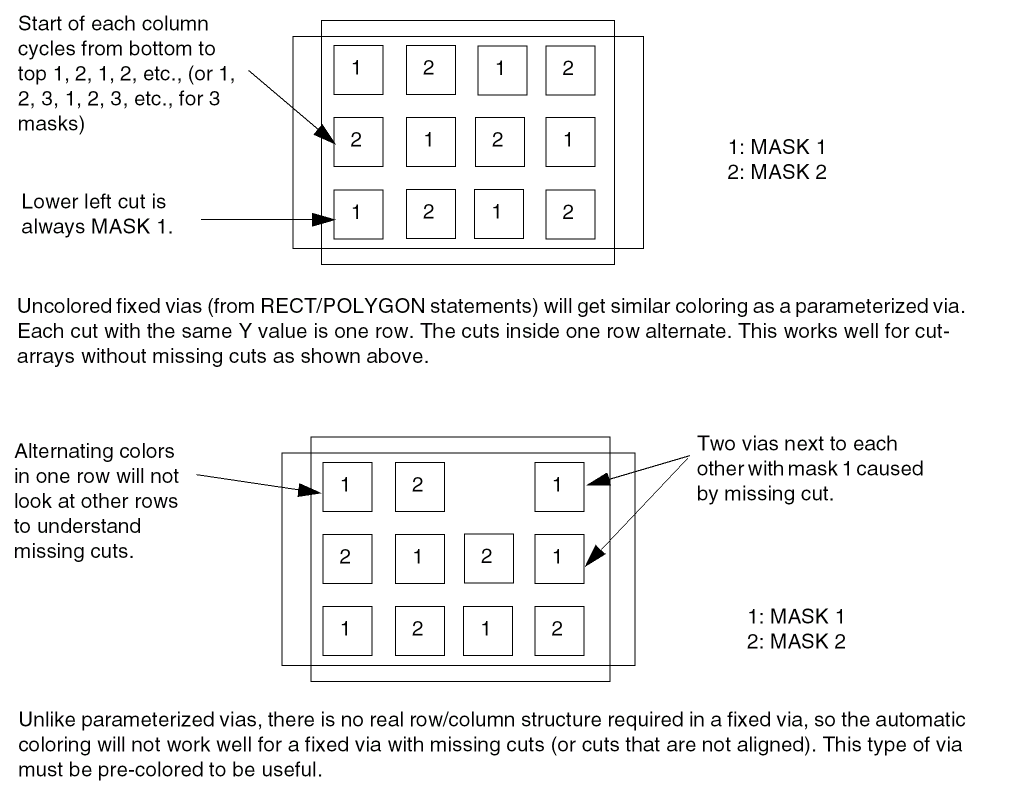
See the MACRO Layer Geometries statement to see how a via-instance uses these via-master mask values.
Via Rule
VIARULEviaRuleNameLAYERlayerName; DIRECTION {HORIZONTAL | VERTICAL} ; [WIDTHminWidthTOmaxWidth;] LAYERlayerName; DIRECTION {HORIZONTAL | VERTICAL} ; [WIDTHminWidthTOmaxWidth;] {VIAviaName;} ... [PROPERTYpropName propVal;] ...
END viaRuleName
Defines which vias to use at the intersection of special wires of the same net.
VIARULE GENERATE statements to create a via for the intersection of two special wires. In earlier versions of LEF, VIARULE GENERATE was not complete enough to cover all situations. In those cases, a fixed VIARULE (without a GENERATE keyword) was sometimes used. This is no longer required.Example 1-23 Via Rule Statement
In the following example, whenever a metal1 wire with a width between 0.5 and 1.0 intersects a metal2 wire with a width between 1.0 and 2.0, the via generation code attempts to put a via12_1 at the intersection first. If the via12_1 causes a DRC violation, a via12_2 is then tried. If both fail, the default behavior from a VIARULE GENERATE statement for metal1 and metal2 is used.
VIARULE viaRule1
LAYER metal1 ;
DIRECTION HORIZONTAL ;
WIDTH 0.5 TO 1.0 ;
LAYER metal2 ;
DIRECTION VERTICAL ;
WIDTH 1.0 TO 2.0 ;
VIA via12_1 ;
VIA via12_2 ;
END viaRule1
Via Rule Generate
VIARULEviaRuleNameGENERATE [DEFAULT] LAYERroutingLayerName; ENCLOSUREoverhang1overhang2; [WIDTHminWidthTOmaxWidth;] LAYERroutingLayerName; ENCLOSUREoverhang1overhang2; [WIDTHminWidthTOmaxWidth;] LAYERcutLayerName; RECTptpt; SPACINGxSpacingBYySpacing; [RESISTANCEresistancePerCut;]
END viaRuleName
Defines formulas for generating via arrays. You can use the VIARULE GENERATE statement to cover special wiring that is not explicitly defined in the VIARULE statement.
Rather than specifying a list of vias for the situation, you can create a formula to specify how to generate the cut layer geometries.
VIARULE GENERATE rule that appear in the DEF NETS or SPECIALNETS sections must also appear in the DEF VIA section.
Specifies that the via rule can be used to generate vias for the default routing rule. There can only be one VIARULE GENERATE DEFAULT for a given routing-cut-routing (or masterslice-cut-masterslice) layer combination.
Example 1-24 Via Rule Generate Default
The following example defines a rule for generating vias for the default routing or masterslice rule:
VIARULE via12 GENERATE DEFAULT
LAYER m1 ;
ENCLOSURE 0.03 0.01 ; #2 sides need >= 0.03, 2 other sides need >= 0.01
LAYER m2 ;
ENCLOSURE 0.05 0.01 ; #2 sides need >= 0.05, 2 other sides need >= 0.01
LAYER cut12 ;
RECT -0.1 -0.1 0.1 0.1 ; # cut is .20 by .20
SPACING 0.40 BY 0.40 ; #center-to-center spacing
RESISTANCE 20 ; #ohms per cut
END via12
Specifies that the via must be covered by metal on two opposite sides by at least overhang1, and on the other two sides by at least overhang2 (see Figure 1-63). The via generation code then chooses the direction of overhang that best maximizes the number of cuts that can fit in the via.
ENCLOSURE rules for the cut layer that apply to a given via, the via generation code will choose the ENCLOSURE rule with values that match the ENCLOSURE in VIARULE GENERATE. If there is no such match, the via generation code will ignore the ENCLOSURE in VIARULE GENERATE and choose which ENCLOSURE rule is best in LAYER ENCLOSURE values that apply to the same width via being generated. This means that only ENCLOSURE statements in LAYER CUT are honored, and one of them will be used.
For example, VIARULE GENERATE ENCLOSURE 0.2 0.0 combined with a LAYER CUT rule of ENCLOSURE 0.2 0.0, ENCLOSURE 0.1 0.1 and ENCLOSURE 0.15 0.15 WIDTH 0.5, would mean that any via inside a wire with width that is greater than or equal to 0.5 wide, 0.15 0.15 enclosure values are used. Otherwise, 0.2 0.0 enclosure values are used. See the LAYER CUT ENCLOSURE statement for more information on handling multiple enclosure rule.
Type: Float, specified in microns
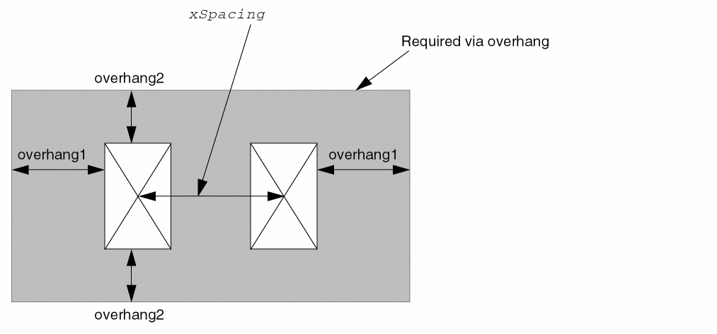
Example 1-25 Via Rule Generate Enclosure
The following example describes a formula for generating via cuts:
VIARULE via12 GENERATE
LAYER m1 ;
ENCLOSURE 0.05 0.01 ; #2 sides must be >=0.05, 2 other sides must be >=0.01
WIDTH 0.2 TO 100.0 ; #for m1, between 0.2 to 100 microns wide
LAYER m2 ;
ENCLOSURE 0.05 0.01 ; #2 sides must be >=0.05, 2 other sides must be >=0.01
WIDTH 0.2 TO 100.0 ; #for m2, between 0.2 to 100 microns wide
LAYER cut12
RECT -0.07 -0.07 0.07 0.07 ; #cut is .14 by .14
SPACING 0.30 BY 0.30 ; #center-to-center spacing
END via12
The cut layer SPACING ADJACENTCUTS statement can override the VIARULE cut layer SPACING statements. For example, assume the following cut layer information is also defined in the LEF file:
LAYER cut12
...
SPACING 0.20 ADJACENTCUTS 3 WITHIN 0.22 ;
...
The 0.20 μm edge-to-edge spacing in the ADJACENTCUTS statement is larger than the VIARULE GENERATE example spacing of 0.16 (0.30 − 0.14). Whenever the VIARULE GENERATE rule creates a via that is larger than 2x2 cuts (that is, 2x3, 3x2, 3x3 and so on), the 0.20 spacing from the ADJACENTCUTS statement is used instead.
VIARULE GENERATE is center-to-center spacing, whereas the spacing in ADJACENTCUTS is edge-to-edge. Defines a formula for generating the appropriate via.
Specifies the cut layer for the generated via.
Specifies the routing (or masterslice) layers for the top and bottom of the via.
Specifies the location of the lower left contact cut rectangle.
Specifies the resistance of the cut layer, given as the resistance per contact cut.
Default: The resistance value in the LAYER (Cut) statement
Type: Float
Defines center-to-center spacing in the x and y dimensions to create an array of contact cuts.The number of cuts of an array in each direction is the most that can fit within the bounds of the intersection formed by the two special wires. Cuts are only generated where they do not violate stacked or adjacent via design rules.
Note: This value can be overridden by the SPACING ADJACENTCUTS value in the cut layer statement.
Specifies the name for the rule.
The name DEFAULT is reserved and should not be used for any via rule name. In the LEF and DEF VIA definitions that use generated via parameters, the reserved DEFAULT name indicates the via rule with the DEFAULT keyword.
Specifies a wire width range to use for this VIARULE. This VIARULE can be used for wires with a width greater than or equal to (>=) minWidth, and less than or equal to (<=) maxWidth for the given routing (or masterslice) layer. If no WIDTH statement is specified, the VIARULE can be used for all wire widths on the given routing (or masterslice) layer.
Return to top