Benefits of Defining Pin Connectivity
The ability to define connection types for pins can be useful if:
- You are a library developer designing a library device for use in a block or circuit design and need to provide layout designers with maximum flexibility by defining some connections internally and leaving other connections to be completed at the next level of design.
- You are a layout designer using a device designed by others in a layout and need to specify, later in the layout cycle, which pins to connect externally.
The following examples show how the ability to define pins as must connects, strongly connected, weakly connected, or pseudo parallel connects can make the design process more efficient for both these job functions.
For Library Developers
If you are working as a library developer, a typical device might be a multi-fingered FET as shown in the following figure.
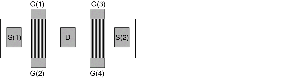
- G(1) and G(2) are weakly connected (inside the device)
- G(3) and G(4) are weakly connected (inside the device)
- The pair G(1)/G(2) must be externally connected to the pair G(3)/G(4)
- S(1) must be externally connected to S(2)
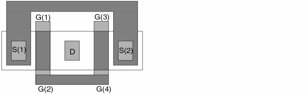
To use this device in a design, if no external (must-connect) connections are defined, you must make internal (strongly connected) connections so the cell looks like this:
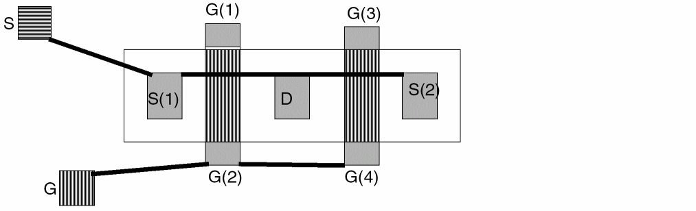
Then, when this device is used in a design, the flight lines look as shown in the following figure:
If the layout designer makes connections between G and G(2) or G(4), the layout editor accepts the connection as complete. If the layout designer makes connections between S and S(1) or S(2), the layout editor accepts the connection as complete.
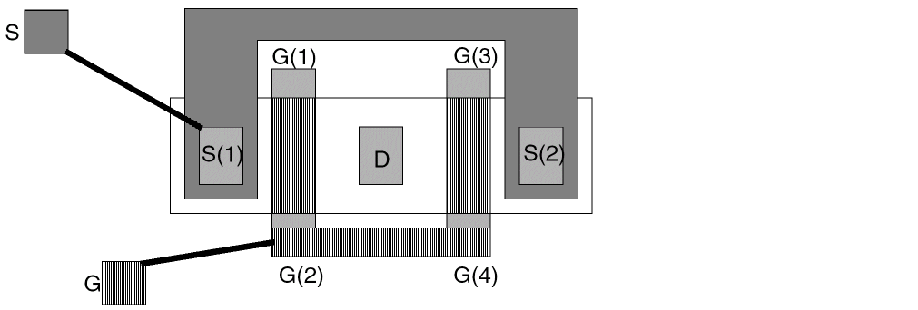
If you, as a library developer, do not want to complete the connections to the source or gate inside the device, but want the connections made at the next level of hierarchy, you do not wire internal connections. Then, when the cell is used in a design, the flight lines look as shown in the following figure:
If the layout designer makes a connection between S and S(1), the software does not accept the connection as complete and displays a flight line to S(2). If the layout designer makes a connection between G and G(2), the software does not accept the connection as complete and displays a flight line to G(4).
If you make a connection between G and G(2) and G(4), the software accepts the connection as complete and displays no more flight lines on this net, because G(1) and G(3) are weakly connected to G(2) and G(4) respectively.
If you make a connection between G and G(2), and between G(1) and G(3), this is considered an error and is indicated by a marker. The software would not accept the internal weak connection between G(1) and G(2) to complete the net.
For Layout Designers
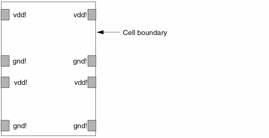
If you are working as a layout designer, a typical design might be a two-row-high standard cell layout as shown below.
Floorplanning information regarding external connections is provided on the boundary of the design by an outside source, such as a circuit designer or library. Given that information early, you can identify which pins must be must connects, strong connects, or weak connects, and can use that information for device placement and wiring.
If you define no external connections, the flight lines look as shown below:
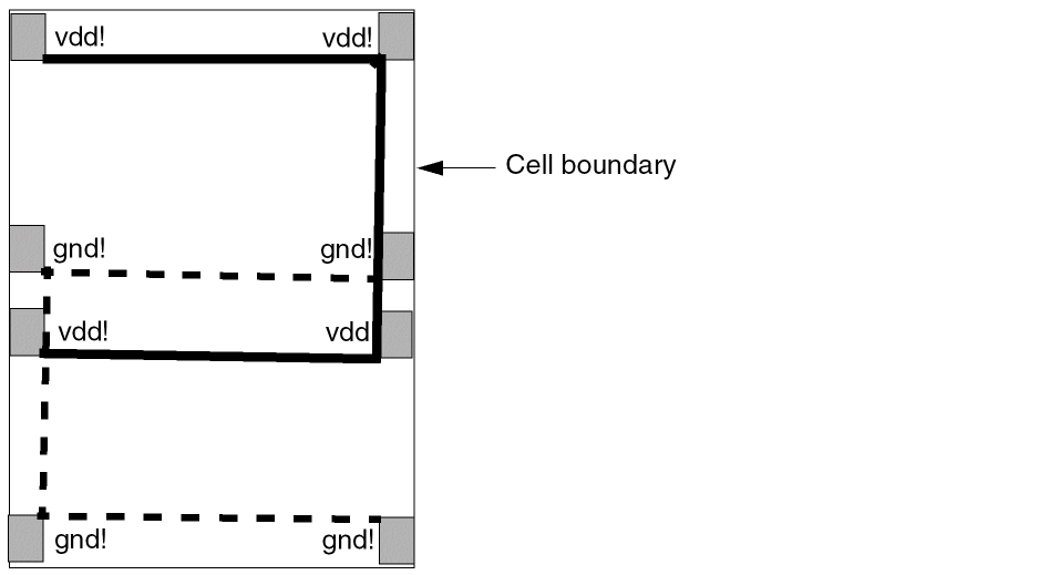
The library developer usually does not connect the top two vdd! pins to the bottom two vdd! pins but does connect the top two vdd! pins together. The same is true for the gnd! pins. So, the library developer defines the top two vdd! pins as being externally connected to the bottom two vdd! pins and the same for the gnd! pins. Then, when you are working inside the cell, the flight lines look as shown below:
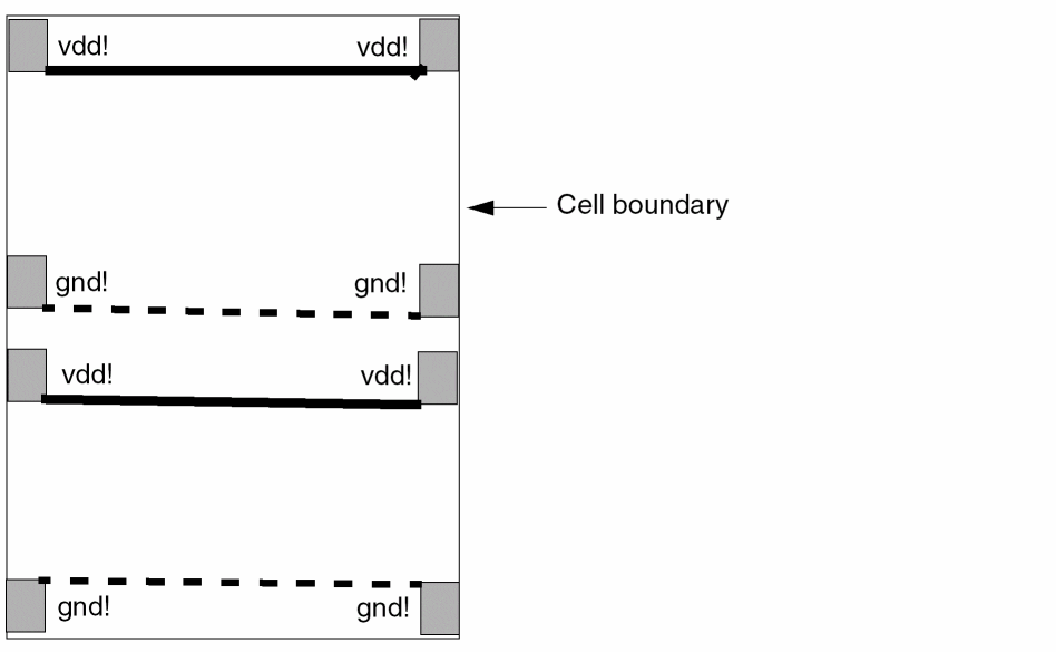
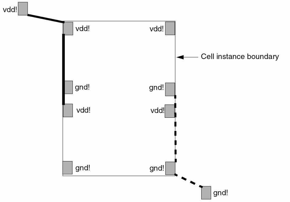
When you use the cell in the next level of hierarchy, the flight lines look as shown in the following image. You must make the connections as shown by the flight lines. You are provided information regarding pin connections by an outside source, such as a circuit designer or library.
Related Topics
Return to top