|
Keyword
|
Option Set
|
Explanation
|
Default Value
|
|
net
|
name=[instance1.net1instance1.net2....]
|
Defines the nets for which the analysis is performed. instance defines the instance of the subcircuit containing the net. net defines the net name inside the subcircuit instance as it is defined in the DSPF *| NET definition. If the DSPF file is included on the top level, the instance name is not required. Wildcarding is supported for net names but not instance names.
|
none
|
|
analysis=[imax iavg iavgpos iavgneg iavgabs iacpeak irms vmax vavg]
|
peakEM, avgEM, avgEM for i>0, avgEM for i<0, avgabsEM, rmsEM, peakIR, avgIR
Note: To perform AC-Peak analysis in Voltus-Fi-XL, ensure that the imax and iavg options are specified in the control file.
|
iavg, vmax
|
|
|
pwrgate=[powernet1 powernet2...]
|
Enables power gate handling. You need to specify the power supply net driving the power gate and the internal power supply net driven by the powergate. If one power supply net drives multiple power gates, then you need to specify one statement with all internal power supply nets. For example:
If the internal and external net names are as follows and XTOP is the top cell name:
pair1 ->[VDD VSS]
pair2 ->[VDDM VDDM1]
pair3 ->[VDDM VDDM2]
Then the following settings can be specified where the second setting will not override the first:
pwrgate=[XTOP.VDD XTOP.VSS]
pwrgate=[XTOP.VDDM XTOP.VDDM1 XTOP.VDDM2]
|
none
|
|
|
analysis=[sigvmax sigvavg] reftype=[avg max]
[findsrc=yes]
|
sigvmax - max signal net IR drop.
sigvavg - avg signal net IR drop.
avg - reference voltage for IR drop is the average voltage of all subnodes at every time point.
max - reference voltage for IR drop is the maximum voltage of all subnodes at every time point.
findsrc=yes - Use voltage from subnode which is connected to vsource. The feature automatically traces through the design or source resistors.
|
none
|
|
|
For versions before MMSIM/SPECTRE15.1 ISR2, the syntax is as follows:
design_res_models=[name=<cell_name> w=<width parameter name> l=<length parameter name> layer=<layer name> unit=<multiplier to get length/width * geounit in um>]
For MMSIM/SPECTRE15.1 ISR2 and later versions, the syntax is as follows:
design_res_models=[name=<cell_name> w=<width parameter name> l=<length parameter name> layer=<layer name> unit=<multiplier to get length/width in m>]
|
Specifies the design resistor models for which EMIR analysis will be performed.
Note: The design resistor models are specified for cells and not for the instances of the cell.
For example, for the design resistor provided in the xDSPF file as:
XR1 XR1#PLUS XR1#MINUS r_user wr=1e-06 lr=5e-06
In this example, width (wr) and length (lr) are in meters.
The design resistor models will be specified in the following manner:
Before MMSIM/SPECTRE15.1 ISR2,
design_res_models=[name=r_user w=wr l=lr layer=mt1 unit=1e6]
MMSIM/SPECTRE15.1 ISR2 and later:
design_res_models=[name=r_user w=wr l=lr layer=mt1 unit=1]
where,
r_user is the design resistor model name
lr is the length parameter name specified in the xDSPF
wr is the width parameter name specified in the xDSPF
mt1 is the layer for the EM rules. The tool will apply mt1 layer rules from the ICT file for this resistor
|
none
|
|
|
|
Before MMSIM/SPECTRE15.1 ISR2
1e6 is the unit that is calculated as design resistor W/L in netlist * unit/geounit. For example:
For lr=5e-06 and unit=1e6, the length value of design resistor in um is as follows:
l=5e-06*1e06=5um
MMISM15.1ISR2 and later
1 is the unit that is calculated as design resistor W/L in netlist * unit. For example:
For lr=5e-06 and unit=1, the length value of design resistor in meters is as follows:
l=5e-06*1=5e-06m
|
|
|
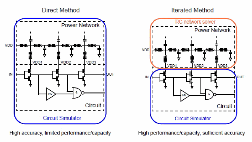
solver
|
method=[auto | direct | iterated | profonly | iteronly]
|
auto - direct for APS, iterated for XPS (default)|
direct - forced direct method, not available for XPS
iterated - forced iterated approach, available for APS and XPS
profonly - iterated flow - circuit profile generation
iteronly - iterated flow - RC network iteration
|
auto
|
|
|
speed=[1|2|3|4|5|6|7|8]
|
Defines the speed/accuracy trade-off for PN and SN RC network solver.
1 - highest accuracy, lowest speed
8 - lowest accuracy, highest speed
|
5
|
|
|
inputwf=file_name
|
Specifies the waveform file that contains the results from circuit simulation when method=iteronly is used.
|
none
|
|
|
report_tapi=on
|
Specifies to generate tap current reports. When this option is specified, outputs the rms, avg, and max tap currents in the .emir#_bin simulation result file.
|
none
|
|
static
|
ifile=”filename”
|
Enables static EMIR analysis. The file defines the subckt instance port currents.
Note: Static EMIR analysis cannot be combined with the dynamic EMIR analysis.
|
none
|
|
|
analysis=[ipwc] pwc_threshold=1e-6
|
Enables pulse-wise EM current calculation for violation visualization. The pwc_threshold option defines the current threshold for finding the start of the pulse. Any value below pwc_threshold is considered as zero. The emirutil_dump_pwc_info=1 option generates an ascii report in the <name>.pwc0_raw file for debugging purpose only.
|
none
|
|
|
vref
|
Defines the optional voltage reference value for vmax and vavg analyses.
|
none
|
|
emirutil
|
techfile="emDataFile"
|
Specifies the EM rule file in the emdatafile, qrctechfile, or ictfile format. Layer names that are not case-sensitive are supported, allowing easier match between the DSPF and emData file.
The EM rule file can be predefined in the configuration file using the EMTECHFILE environment variable or in the .cdsinit file as follows:
envSetVal("spectre.envOpts" "emTechFile" string <path to the file>
The rule file defined in the configuration file has a higher priority followed by the rule file specified in .cdsinit.
Alternatively, you can use the emdatafile="emDataFile" option to specify the techfile in the emdata format, qrctechfile="qrcTechFile" to specify the Quantus tech files, and ictfile="ictfile" to specify the file in the ICT format.
The EM rule file in emdatafile format can be predefined using the EMDATAFILE environment variable, or emRuleFile in cdsenv. The EM rule file defined in cdsenv has a higher priority.
|
none
|
|
|
|
The layermap file provides the mapping between the xDSPF and the layout database. It is applicable only for qrcTechfile and ictfile.
|
|
|
|
EMOnlyICTFile=”emOnlyICTFile”
|
Specifies the process and EM models to be used for EM analysis.
Note: This file can only be provided with the qrcTechFile flow.
|
none
|
|
|
res_pdata_sw=[on]
|
When the bounding box coordinates are included in the xDSPF file and this option is set to on, prints the coordinates of resistor bounding box in the electromigration report. If this option is not specified in the EMIR conf file or the coordinates are not included in xDSPF, the node coordinates of resistors are printed instead of the bounding box coordinates.
|
none
|
|
|
rcIrcxFile=[./RC_your_file.ircx]
|
Specifies the RC iRCX file provided by the foundry to be used for EM analysis.
|
none
|
|
|
emirIrcxFile=[./EMIR_your_file.ircx]
|
Specifies the EMIR iRCX file provided by the foundry to be used for EM analysis.
|
none
|
|
|
ir_in_em=[true | false]
|
When set to true, reports the maximum IR drop value for each metal resistor/via in the EM current report. It adds a “Max IR” column in the EM report.
|
false
|
|
|
tap_model_report=yes | no
|
When set to yes, the software reports the device model names for all the tap devices in the dynamic and static analysis report files – *.rpt_ir and *.spgs.
|
none
|
|
|
layerSetupFile=filename
|
Specifies the name of the layer setup file to be used for the Voltus-Fi Quantus shape server flow.
By default, the Voltus-Fi Quantus shape server flow reads the “layer_setup” file from the path specified in the "_qrc_tech_dir" file of the qrc run dir.
Use this option to specify a file other than the default file.
For example:
emirutil layerSetupFile=layer_setup_1
|
none
|
|
|
mdLayers=”mdlayer1 mdlayer2 mdlayer#”
|
Specifies the list of metal diffusion layers that need to be combined for EM analysis. For example, to calculate the distance between terminal vias (Lv2v), for thermal analysis (SHE) and so on.
The default value is shown below.
emirutil mdLayers=”MD_STI MD_OD MD_STI_SRM MD_OD_SRM M0_OD M0_STI MD_STI_CPP85 MD_OD_CPP85”
|
MD_STI MD_OD MD_STI_SRM MD_OD_SRM M0_OD M0_STI MD_STI_CPP85 MD_OD_CPP85
|
|
|
mergeMDLayers=[true | false]
|
Enables combining of metal diffusion layers that are specified using the variable, mdLayers, for calculating the effective Blech length. When set to false, no merging of metal diffusion layers is done for the Blech length calculation.
emirutil mergeMDLayers=true
|
true
|
|
|
mt=8
|
Specifies the number of CPUs used by clients for multithreading.
emirutil mt=8
|
8
|
|
|
postTclCmdFile=[conf.tcl]
|
Specifies the Tcl file that contains user-specified commands for querying specific resistor and node information and creating customized EM and IR drop analysis reports.
For details about the commands that can be written in the file (conf.tcl), see the “Batch Mode Execution” chapter.
|
none
|
|
|
layermapfile=”mapfile”
|
Specifies the layer map file that provides the mapping between the layer names in the simulation database to the layer names in the technology file.
|
none
|
|
|
layermap=[(rcxLayer=rcx_layer_name1 ictLayer=ict_layer_name1) (rcxLayer=rcx_layer_name2 ictLayer=ict_layer_name2)]
|
Specifies the mapping between the layer names in the simulation database to those specified in the technology files (qrcTechFile and ICT file) for the EM analysis flow. It maps the layer names in the xDSPF file to the ICT layer names.
rcxLayer is the layer name in the simulation database.
ictLayer is the layer name in the ICT EM file.
Example:
emirutil layermap=[(rcxLayer=M1 ictLayer=T1) (rcxLayer=M2 ictLayer=T2)]
|
none
|
|
|
autorun=[true | false]
|
true - run emirutil automatically to generate a text report.
false - manually run emirutil.
|
true
|
|
|
reportCurrentAmp=[true | false]
|
true - reports the current of the resistor in ampere (A).
false - reports the current of the resistor in milliampere (mA).
|
true
|
|
|
report=[text | html | csv]
|
Defines the type of report created by emirutil.
text - creates a report in text format.
html - creates the report in HTML format.
csv - creates the report in CSV format.
Note: Multiple entries are supported.
|
text
|
|
|
report_voltage=[true | false]
|
When set to true, IR reports display the absolute voltage value instead of the IR drop value and in the GUI, the Virtuoso layout displays the absolute voltage plots instead of the voltage drop plots.
emirutil report_voltage=true
|
false
|
|
|
notation=[s | e]
|
Notation for the text and html reports.
e - engineering scale number (for example, 5.02m)
s - scientific notation (for example, 5.02e-3)
|
e
|
|
|
sort_by_net=yes|no
|
Report IR and EM results per net, or all nets.
yes - report EMIR results per net
no - combine EMIR results or all nets into one report.
|
yes
|
|
|
power_gate_extra_report
|
When specified, adds additional information in the rpt_pwg file about power gates.
This option is used only for power-gated designs.
|
none
|
|
|
filter_ir_
threshold=
value
|
Defines the IR voltage drop threshold for the node being reported.
filter_ir_threshold=0.01 reports all nodes with IR drop above 0.01V.
|
no filter
|
|
|
filter_ir_
percent=
value
|
Defines the percentage of nodes being reported starting from the biggest IR drop. For example, filter_ir_percent=5 reports the top 5 percent IR drop nodes in the report.
|
no filter
|
|
|
filter_em_threshold=value
|
Defines the EM analysis threshold value for the resistors being reported. The value for filter_em_threshold is the J/Jlimit value.
filter_em_threshold=1 reports only those resistors that have a J/Jlimit value above 1.
Note: Specifying this option is equivalent to filtering all passed resistors.
|
none
|
|
|
filter_resistance=0.001
|
Specifies that the shorting via resistors with the resistance value equal to or less than 0.001 ohm (1 mohm) are to be filtered out from the EMIR and SHE analysis reports.
|
none
|
|
|
geounit=value
|
Defines the scaling of all DSPF geometry parameters (W, L, X, Y). It applies only to the *|NET section, and not to the instance section.
|
1um
|
|
|
geounit_XY
|
Defines the scaling of DSPF geometry parameters X and Y. It applies only to the *|NET section, and not to the instance section.
Note: If the geounit_XY and geounit options are specified together, the geounit_XY option takes precedence over the geounit option.
|
1um
|
|
|
geounit_WL
|
Defines the scaling of DSPF geometry parameters W and L. It applies only to the *|NET section, and not to the instance section.
Note: If the geounit_WL and geounit options are specified together, the geounit_WL option takes precedence over the geounit option.
|
1um
|
|
|
enableDesignResistorPeakFactor= [true | false]
|
Specifies the addition of the factor, 1/(r)1/2, in the current limit calculation for the AC-Peak analysis of the design resistor.
The software, by default, calculates the current limit for the AC-Peak analysis of the design resistor using the following equation:
Ipeak_ac(limit)= Ipeak_dc(limit)
To apply the factor, 1/(r)1/2, in your calculation, set this variable to true. The current limit will then be calculated in the following manner:
Ipeak_ac(limit)= Ipeak_dc(limit)/(r)1/2
|
false
|
|
|
enableDesignResistorScaling=[true | false]
|
Enables the scaling of the width and length values based on the layout_scale factor specified in the technology file before the EM rules are applied for EM analysis of design resistors.
By default, the scaling of design resistors is enabled.
|
true
|
|
|
enableResShape true | false
|
When set to true, enables tagging of shapes on the layout based on full resistor shapes and terminal nodes. This option is enabled by default. To disable tagging of shapes, set the variable to false.
emirutil enableResShape false
|
true
|
|
|
enableRMSHotSpotWaiving=[true | false]
|
Enables the RMS EM hot spot waiving analysis. By default, this feature is disabled.
|
false
|
|
|
extendPWLMatch=[true | false]
|
When the EM rules are specified in terms of PWL and the width of metal or the area of via does not match with any width/area of the PWL, the EM limit will not be calculated for this metal resistor/via.
When set to true, the software interpolates the limit value for the resistor/via from the selected rule PWL as follows:
minimum of PWL ith value * (metal's width or via's area) / (PWL ith width or PWL area).
|
false
|
|
|
enablePWLDensityInterpolation=[true | false]
|
Enables the current density calculation from the given PWL using current density and width, or current density and area linear interpolation for either the metal's width or the via's area. The calculation is only done when the metal’s width or the via’s area does not match the PWL width or area values.
emirutil enablePWLDensityInterpolation=true
|
false
|
|
|
viaCountResistance=[true | false]
|
This option is set to true when third-party DSPF with missing via count ($N) is used for EM analysis.
|
false
|
|
|
process_scale=value
|
Specifies the value by which the width and length values will be multiplied before the EM rules are applied.
|
1.0
|
|
|
prioritizedPwlRulesLayers=[all | none | list_layers]
|
Specifies the list of layers for which area-based PWL search is performed first. When no match is found, then non-PWL rules are used. The default value of this variable is “all”, which means that this behavior is enabled for all layers.
To enable the behavior for specific layers, you can specify a list of layers.
To disable this behavior for all layers, set the value of this variable to none. In the GUI, you can set this variable in the Variables form.
Example rules:
em_jmax_dc_avg 10 jmax_factor 90 2.384 95 2.078 - non-PWL baseline rule
em_jmax_dc_avg PWL 0.3582 0.001444 0.5694 0.003364 0.7164 0.0038 jmax_factor 90 2.384 - PWL rule
When both the above rules are specified, the second rule is given priority over the first.
|
all
|
|
|
via_count=[useR | useArea]
|
Defines the method used for calculating the via count.
useR - calculation based on via resistance (emdatafile_via_resistance/dspf_via_resistance).
useArea - calculation based on via area (dspf_via_area/emdatafile_via_area).
|
useR
|
|
|
idirn=[true|false]
|
Prints the current direction in the EM report (Current Direction column). For metal resistors, the current direction is printed. That is, W means that the current is flowing from east to west. For via resistors, the direction from/to layer is printed.
|
false
|
|
|
recovery_factor
|
Defines the recovery factor for iavg calculation with recovery factor. If specified, then iavg=max(|iavgpos|,|iavgneg|)-recovery_factor*min(|iavgpos|,|iavgneg|).
If not specified, then iavg=iavgpos+iavgneg
|
|
|
|
Tlife=”hours” | “years”
|
Specifies the lifetime for which the EM analysis will be performed. You can specify the value in either years or hours. For example:
emirutil Tlife=”20000hours”
|
“10 years”
|
|
|
emLimitScale=scale_factor_value | “scale_factor_netfile”
|
Scales the EM limits of the parasitic resistors in the design before generating the EM reports. You can either apply the same scale factor to all the nets or specify different scale factors for different nets.
To apply the same scale factor to the parasitic resistors of all the nets in the design, provide the value of the scale factor.
emirutil emLimitScale=scale_factor_value
For example,
emirutil emLimitScale=0.04
Note: This is applicable to avg, avg abs, and rms analyses. For the avg and avg abs analyses, the limit is directly multiplied by this factor. For rms analysis, the limit is multiplied by the root of this factor.
To apply different scale factors to different nets in the design, provide the name of the file that contains information about the net names and the corresponding scale factors to be applied to these nets.
emirutil emLimitScale=”scale_factor_netfile”
For example,
emirutil emLimitScale=“scaleLimitFile”
|
none
|
|
|
rmsMetalLineNumberPower=number
|
Specifies the value of power on the metal lines for RMS EM analysis of power nets.
If this option is not specified, the default value of 0 is considered, which means the software uses the em_dc_rms_metal_line_num value specified in the ICT file.
If, however, this option is specified, it overrides the em_dc_rms_metal_line_num value specified in the ICT file.
|
0
|
|
|
rmsMetalLineNumberSignal=number
|
Specifies the value of power on the metal lines for RMS EM analysis of signal nets.
If this option is not specified, the default value of 0 is considered, which means the software uses the em_ac_rms_metal_line_num value specified in the ICT file.
However, if this option is specified, it overrides the em_ac_rms_metal_line_num value specified in the ICT file.
|
0
|
|
|
print_em_report
|
Defines the EM analysis report file to be generated in the Voltus-Fi-XL flow.
filename: create report with specified filename
net: create report for specified nets - all power nets (all_power), all signal nets (all_signal), all nets (all_nets), or net (netname).
threshold - create report for resistors or nodes that have a threshold value of EM ratio above the specified value
type - create report for specified analysis type; javg, jmax, jabsavg, jacpeak, jacrms, rc, rcavg, rcrms, tc, tcavg, or tcrms.
rule - specifies the custom EM rule for which the report should be generated
|
|
|
|
extendedreport=true | false
|
Specifies that the following information should be included in the EM analysis report file:
-
Td: time duration in micro second or total ‘On Time’ period -
dutyR: duty ratio -
Ilimit: current limit
|
false
|
|
|
extendedRMSReport=true | false
|
When set to true, the following parameters are reported in the RMS EM report:
-
rmsT: Delta temperature value -
Lv2v: Distance between terminal vias -
rmsMetalLineNumRelaxFactor: It specifies the rating factor corresponding to the number of power on metal lines
In addition, the following is added in the header section of the report:
-
rmsMetalLineNumber: Specifies the value of power on the metal lines for RMS EM analysis
|
false
|
|
|
reportUnmatchedRuleResistor=true | false
|
When set to true, specifies that while generating the EM analysis reports, the resistors that do not match any EM rule for the specified analysis in the ICT file should be reported in the “#.rpt_unmatch” file.
|
true
|
|
|
reportAllResistor=true | false
|
When set to true, reports all resistors of the specified nets in the “#.rpt_all” file.
|
false
|
|
|
consolidatedReport=true
|
Specifies that consolidated EM and IR reports for multiple bin files will be generated in Voltus-Fi-XL.
|
false
|
|
|
worstResult=true
|
Specifies that the worst result will be reported in the consolidated EM and IR reports. This option is enabled by default when the consolidatedReport parameter is set to true.
For example,
consolidatedReport=true
worstResult=true
|
true
|
|
|
layer_filter=[layer1 layer2...]
|
Specifies the layers that are to be filtered out from the EMIR analysis reports.
For example,
emirutil layer_filter=[cont odcont]
|
none
|
|
|
violation_columns=[column_names]
|
Specifies the columns to be displayed in the Violation Browser. You can specify multiple columns separated by a space from the following list of columns:
LENGTH_COLUMN
RESISTANCE_COLUMN
VIA_AREA__COLUMN
NEEDED_NUM_VIA_COLUMN
NET_COLUMN
WIDTH_COLUMN
MIN_WIDTH_COLUMN
DENSITY_COLUMN
CURRENT_LIMIT_COLUMN
CURRENT_COLUMN
PEAK_TIME_COLUMN
TAP_NAME_COLUMN
For example,
emirutil violation_columns=[LENGTH_COLUMN RESISTANCE_COLUMN]
|
All columns are displayed
|
|
|
disableLayoutScale=true
|
When set to true, disables the layout scale factor defined in the ICT file for Voltus-Fi-XL EM analysis. The layout_scale factor is the ratio of the scaled dimensions divided by the drawn dimensions.
The ICT file is defined based on the scaled dimensions. Quantus applies the layout_scale factor to the input design during extraction so that the design dimensions and the ICT file dimensions are consistent.
|
false
|
|
|
simpleSingleViaDefinition=true | false
|
The keyword, single is used to differentiate between a single square cut via and square via array. It is applicable to square via, with width equal to 'vc_width/min_width', only.
To support the single keyword for all via sizes, set the simpleSingleViaDefinition parameter to true.
|
false
|
|
|
cdf_percentage=value
|
The variable holds the value which is mapped to the cdf_percentage keyword in the EM rules specified in the ICT file or the technology file.
The value of the cdf_percentage should be between 0 and 100.
For example,
emirutil cdf_percentage=”10.0”
|
none
|
|
|
device_temp_file=filename
|
Specifies the file that includes information about resistor names and their corresponding temperature values. The EM analysis for these resistors is performed at their corresponding temperatures.
For example,
emirutil device_temp_file=resistor_temp.txt
|
none
|
|
|
toggleNetFrequency=”(net1, frequency1) (net2, frequency2) (net#, frequency#)”
|
Specifies the frequency of the nets so that the tool can derive the Td (total on-time period) for multiple clock cycles. You can specify frequencies for different nets as shown below. Wild cards are also supported.
For example,
emirutil toggleNetFrequency=”(CLK*,2.3e9) (NET1,4.6e9)”
|
none
|
|
|
toggleNetFrequencyFile=filename
|
Specifies the name of the file that contains the net names and their corresponding frequency values. This file is used to specify the frequency of nets to compute the Td (total on-time period) for multiple clock cycles. This file contains net names separated by commas and the frequency values.
For example,
emirutil toggleNetFrequencyFile=freq_file
A sample freq_file is shown below.
VDD, 2e08
D*, 4e08
GSS, 3e08
|
none
|
|
|
multiplePeakPercentThreshold=value
|
Specifies the threshold percentage for the peak current above which the Td (total on-time period) for a particular peak is added to the final Td.
For example,
emirutil multiplePeakPercentThreshold=7
|
5
|
|
|
deltaT=temp_value
|
Specifies the maximum rise in temperature in degree Celsius, caused due to Joule heating. It must be a positive value.
If the rise in temperature is not specified, Voltus-Fi-XL considers a default temperature of 5 degrees Celsius. This is an ideal condition wherein the design must be EM free.
Example:
emirutil deltaT=4.0
This option can also be specified in the Variables form and in the command file by using the set_variable command.
|
5.0 degree Celsius
|
|
|
deltaTLayers=[(layer=layer_name deltaT=temp_value) (layer=layer_name deltaT=temp_value)]
|
Specifies layer-specific deltaT values. For layers that do not have deltaT value specified for them, global deltaT value will be used.
Example:
emirutil deltaTLayers=[(layer=rhim hi_em=1 deltaT=25) (layer=rhim hi_em=0 deltaT=5) (layer=M7 deltaT=10)]
In the above example, hi_em=1 indicates high current carrying design resistor for which the deltaT value is 25 degree Celsius while hi_em=0 indicates general design resistor for which the deltaT value is 5 degree Celsius. The deltaT value for M7 layer is 10 degree Celsius.
This option can also be specified in the Variables form and in the command file by using the set_variable command.
|
none
|
|
|
resistor_filter=[resistor_names]
|
Filters the specified resistors in the plot. You can specify multiple resistors separated by a space. These resistors will not be displayed in the plot. Wildcards are supported.
Example:
emirutil resistor_filter=[rx ry]
or
emirutil resistor_filter=[rx*]
|
All resistors are displayed
|
|
|
exclusion_resistor_filter=[resistor_names]
|
Filters all resistors in the plot except those that are specified. This option is used to view plots for specific resistors. Wildcards are supported.
Example:
emirutil exclusion_resistor_filter=[rx ry]
or
emirutil exclusion_resistor_filter=[rx*]
|
All resistors are displayed
|
|
|
removeBulkShorting=true | false
|
When set to true, this option removes bulk-shorting in the design. Bulk-shorting in the design results in an increase in the EM analysis runtime.
This variable is only used as a troubleshooting option.
Example:
emirutil removeBulkShorting=true
|
false
|
|
|
emVariableValues=[(variable=configA value=#) (variable=configB value=#)]
|
Specifies the EM variable values for current density limit calculation in the EMIR configuration file.
Example:
emirutil emVariableValues=[(variable=configA value=20) (variable=configB value=10)]
Where the values of configA and configB are 20 and 10, respectively.
|
none
|
|
|
enableContextAwareSrmsRelaxation=true | false
|
When set to true, this option enables the context-aware RMS Relaxation flow.
Example:
emirutil enableContextAwareSrmsRelaxation=true
|
false
|
|
time
|
window=[start1 stop1 start2 stop2 ...]
|
Time window to which the EMIR analysis is applied. Multiple none-overlapping windows are supported.
|
[0 tend]
|
|
spf
|
aliasterm="alias library_terminal name"
|
Alias used when DSPF instance terminal names do not match the cell terminal name in the libraries.
|
none
|
|
spgs
|
net=[net1 net2 …]
|
Enables static power grid solver, and defines power nets to be analyzed.
|
none
|
|
|
pwrgate=[powernet1 powernet2 …]
|
Defines power gates to be analyzed in static power grid solver.
|
none
|
|
|
rshort=value
|
Resistors with R<rshort are shorted during static power grid analysis.
|
0
|
|
|
tap2sub net=<net_name> include=[<tap_name>] exclude=[<tap_name>]
|
Converts tap to subnode.
|
none
|
|
|
tap2pin net=<net_name> include=[<tap_name>] exclude=[<tap_name>]
|
Converts tap to pin.
|
none
|
|
|
sub2tap net=<net_name> include=[<node_name>] exclude=[<node_name>]
|
Converts subnode to tap.
|
none
|
|
|
sub2pin net=<net_name> include=[<node_name>] exclude=[<node_name>]
|
Converts subnode to pin.
|
none
|
|
|
pin2sub net=<net_name> include=[<pin_name>] exclude=[<pin_name>]
|
Converts pin to subnode.
|
none
|
|
|
pin2tap net=<net_name> include=[<pin_name>] exclude=[<pin_name>]
|
Converts pin to tap.
|
none
|