8
Technology File Devices
This chapter contains the following topics pertaining to technology file devices:
- devices
- tcCreateDeviceClass
- tcDeclareDevice
- tcDeleteDevice
- tfcDefineDeviceProp
- tcCreateCDSDeviceClass
- cdsViaDevice
- ruleContactDevice
- multipartPathTemplates
- waveguideTemplates
- extractMOS
- extractRES
- extractCAP
- extractDIODE
devices
devices()
Description
Is the technology file devices section enclosure. It is used to activate the Cadence predefined device types, declare devices of those types, and specify multipart path templates.
After activating the Cadence predefined device classes with tcCreateCDSDeviceClass, you can specify the following in the devices section of the technology file:
-
cdsViaDevice declares a
viadevice. -
ruleContactDevice declares a
rule contactdevice. - multipartPathTemplates defines a template or a set of templates that specify relative object design (ROD) multipart paths (MPPs).
- waveguideTemplates defines a template or a set of templates that help generate waveguides.
Additionally, you can specify the following extract devices:
tcCreateDeviceClass
tcCreateDeviceClass(
t_viewName
t_className
l_classParam
l_formalParam
geometry
) ;tcCreateDeviceClass
Description
Defines a custom device type. The class parameters define the physical characteristics of the device; for example layer-purpose pairs for source, drain, or gate and enclosure values. The formal parameters are those that you want to be able to modify when you place the device. The geometry portion of the device type definition is SKILL code that defines the rectangles, lines, nets, terminals, and pins that make up the device type.
tcDeclareDevice statements that use the device type. Moreover, you must use a new tcCreateDeviceClass subclass for every custom device type that you create.Arguments
Example 1
; Create "syMGEnhancement" device class
;
tcCreateDeviceClass("symbolic" "syMGEnhancement"
; class parameters
   ( (sdLayer "hilite") (gateLayer "hilite")
     (sdExt 0.0) (gateExt 0.0)
     (sdImpLayer nil) (sdImpEnc 0.0) )
; formal parameters
   ( (width 0.0) (length 0.0) )
; geometry
    W2 = width/2  L2 = length/2
    netId = dbMakeNet(tcCellView "G")
    dbId = dbCreateDot(tcCellView gateLayer -W2-gateExt:0)
    dbId = dbCreatePin(netId dbId "gl")
    dbSetq(dbId list("left") accessDir)
    dbId = dbCreateDot(tcCellView gateLayer W2+gateExt:0)
    dbId = dbCreatePin(netId dbId "gr")
    dbSetq(dbId list("right") accessDir)
    dbId = dbCreateRect(tcCellView gateLayer
        list(-W2-gateExt:-L2 W2+gateExt:L2))
    dbAddFigToNet(dbId netId)
    ;
    netId = dbMakeNet(tcCellView "S")
    dbId = dbCreateDot(tcCellView sdLayer 0:L2)
    dbId = dbCreatePin(netId dbId "s")
    dbSetq(dbId list("top") accessDir)
    dbId = dbCreateRect(tcCellView sdLayer list(-W2:0 W2:L2+sdExt))
    dbAddFigToNet(dbId netId)
) ; end of syMGEnhancement
Shows a customized device type. When you declare a device of this type with tcDeclareDevice, you specify the values used in a device.
Example 2
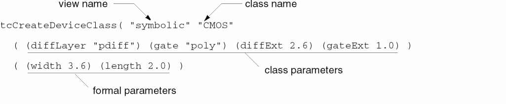
Creates a class called CMOS. The SKILL functions are described in small groups. The entire device class definition appears at the end of this example.
The first line in the following example names the class CMOS and assigns it the view name symbolic (that is, all devices in this class are saved as symbolic cellviews). The closing parenthesis for the tcCreateDeviceClass statement appears at the end of the entire device class definition.
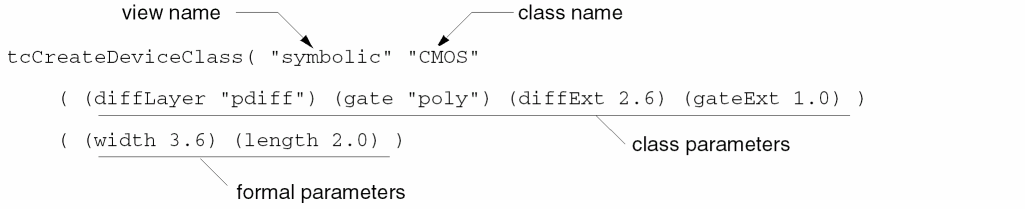
The second line in the figure above lists the class parameters. You can create any parameter name you want and assign it a default value. In this example, the class parameters diffLayer and gate assign the layers on which the device is constructed. The diffExt and gateExt parameters define the amount of extension on the diffusion and gate layers, in microns.
The third line in the figure above lists the formal parameters. Again, you can create any parameter name you wish. The formal parameters appear in the options window when you place instances for this class. You should assign the parameters meaningful names that make sense to the person placing the device. In this example, the formal parameters width and length assign the width and length of the transistor (the area where diffusion and gate intersect), in microns.
The formal and class parameters are followed by the SKILL code that describes how to construct the device. You can use the SKILL database access commands (db commands) for describing database objects to define the rectangles, lines, nets, terminals, and pins required by each device in the class.
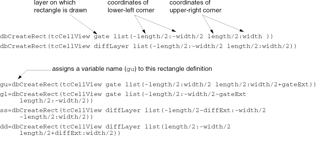
The first line in the following example defines a rectangle on the gate layer. The second line defines a rectangle of the same size on the diffusion layer. Together, these two rectangles make up the active area of the transistor.
In this example, tcCellView is a previously defined global variable that assigns the view name, symbolic. The global variable is defined only while the SKILL code is being run. The remaining four lines define the diffusion and gate extensions, assigning variable names (gu, gl, ss, and dd) to some of the rectangles for use later in this device class definition.
Each succeeding dbCreateRect function call creates a new device variant, a rectangle with tcCellView as the master cellview of the variant. All of the rectangles are defined in relation to the origin (0,0) of the device. For example, given the default length and width values of 2.0 and 3.6, the coordinates of the first rectangle are (-1, -1.8) and (1, 1.8). The resulting rectangle is 2.0 microns wide (the length value) by 3.6 microns high (the width value) and is centered around the origin of the transistor.
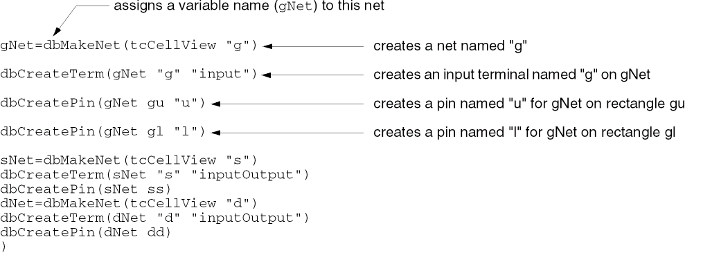
The final section of the SKILL code defines the nets, terminals, and pins required by this device. The first line in the following example defines a new net named g and assigns that net the variable name gNet. The next three lines define one terminal and two pins on this net.
-
The terminal name is
gand its direction isinput. -
The first pin is assigned to the rectangle named
guand given the nameu. -
The second pin is assigned to the rectangle named
gland given the namel.
The last lines define two more nets with a terminal and a pin each. The final parenthesis closes this device class definition.
The resulting default transistor for this class appears as follows:
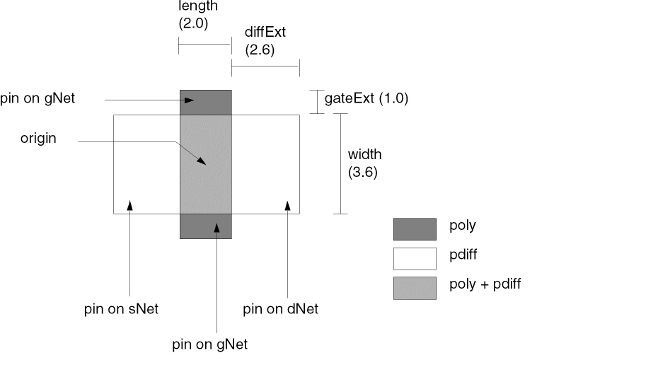
You can change the dimensions and layers for the individual devices in this class as you define devices in the technology file.
The entire set of SKILL functions for this device class is repeated below:
;Section 1
tcCreateDeviceClass(  "symbolic" "CMOS"
  ( (diffLayer "pdiff") (gate "poly")
    (diffExt 2.6) (gateExt 1.0) )
  ( (width 3.6) (length 2.0) )
;
;Section 2
;draw the rectangles for the device
dbCreateRect(tcCellView gate list(-length/2:-width/2 length/2:width/2))
dbCreateRect(tcCellView diffLayer list(-length/2:-width/2 length/2:width/2))
gu=dbCreateRect(tcCellView gate list(-length/2:width/2
     length/2:width/2+gateExt))
gl=dbCreateRect(tcCellView gate list(-length/2:-width/2-gateExt
     length/2:-width/2))
ss=dbCreateRect(tcCellView diffLayer list(-length/2-diffExt:-width/2
     -length/2:width/2))
dd=dbCreateRect(tcCellView diffLayer list(length/2:-width/2
     length/2+diffExt:width/2))
;
;Section 3
;Define nets, pins, and terminals
;Assign pins to previously defined rectangles
gNet=dbMakeNet(tcCellView "g")
dbCreateTerm(gNet "g" "inputOutput")
dbCreatePin(gNet gu "u")
dbCreatePin(gNet gl "l")
sNet=dbMakeNet(tcCellView "s")
dbCreateTerm(sNet "s" "inputOutput")
dbCreatePin(sNet ss)
dNet=dbMakeNet(tcCellView "d")
dbCreateTerm(dNet "d" "inputOutput")
dbCreatePin(dNet dd)
)
tcDeclareDevice
tcDeclareDevice(t_viewName t_className t_deviceName(('s_classParam g_value) …) (('s_formalParam g_value) …)
=> t / nil
Description
Creates the device defined by tcCreateDeviceClass.
Arguments
Example
tcDeclareDevice( "symbolic" "syEnhContact" "myEnhCont"
    ( (viaLayer "Via1") (layer2ImpEnc 0.000000) (layer2ImpLayer (quote nil))
    (layer1ImpEnc 0.450000) (layer1ImpLayer "Nimp") (encByLayer2 0.350000)
    (encByLayer1 0.310000) (layer2 "Metal2") (layer1 "Metal1") )
    ( (w 0.300000) (myProp2 "net2") (myProp1 "net1")
    (yBias "center") (xBias "center") (yPitch 0.800000)
    (xPitch 0.700000) (column 1) (row 2)(l 0.300000) )
)
tcDeleteDevice
tcDeleteDevice(t_viewName t_className t_deviceName[d_techfileID]
)
Description
Deletes a device defined using tcCreateDeviceClass and tcDeclareDevice. This subclass must be placed in the devices class of the technology file after the tcCreateDeviceClass and tcDeclareDevice declarations of the device being deleted.
Arguments
tfcDefineDeviceProp
tfcDefineDeviceProp(
(viewName deviceName propName propValue)
…
)
=> t/nil
Description
Arguments
Example
tfcDefineDeviceProp(
    (symbolic POLYS_M1 res      1.000000 )
    (symbolic M1_M2    res      1.500000 )
    (symbolic M3_M2    viaType  "default")
)
tcCreateCDSDeviceClass
tcCreateCDSDeviceClass()
Description
Activates the Cadence predefined device classes—cdsViaDevice and ruleContactDevice. You can also specify multipartPathTemplates. After the Cadence predefined device classes are activated, you can declare specific devices of these types with the appropriate device specification.
You must place tcCreateCDSDeviceClass() in the devices section before you define any devices by using the Cadence predefined device types.
Example
tcCreateCDSDeviceClass()
Activates the Cadence predefined device types.
cdsViaDevice
cdsViaDevice( (t_deviceNamet_cutLayert_cutPurposet_layer1t_layer1Purposet_layer2t_layer2Purposen_rown_columnt_origing_stackedViasg_cutLayerWg_cutLayerLg_xCutSpacingg_yCutSpacing g_layer1XDirOverrideg_layer1YDirOverride g_layer2XDirOverrideg_layer2YDirOverride t_layer1Dirt_layer2Dir g_layer1XDefOverrideg_layer1YDefOverride g_layer2XDefOverrideg_layer2YDefOverride l_implantLayer1 l_implantLayer2 g_diffSpacing t_abutClass g_useEnclosurePrecision) …
) ;cdsViaDevice
Description
Declares devices of the Cadence predefined via type. A via device is a single contact or array of contacts placed between two layers. This section must be included after tcCreateCDSDeviceClass in the devices section of the technology file.
A cdsViaDevice, rather than a standardViaDef, is required when one or more of the following conditions exist:
-
The via has multiple
layer1and/orlayer2implant layers. - The spacing between the diffusion layers of two vias that cannot abut (g_diffSpacing) must be specified.
-
The via must be assigned an abutment class (t_abutClass).
You can specify cdsViaDevice directly in the technology file, or when you create a substrate tie, the technology file compiler automatically creates cdsViaDevice in the technology file. In either case, the compiler also creates a custom via definition that references the device. If you specify cdsViaDevice when none of the conditions listed above exist and techVersion is not used, the compiler creates a standard via definition and does not create the device.
primaryShapePurpose, cutShapePurpose, and otherShapePurpose, with default value "" (an empty string), can be used to override the purpose when creating a cdsVia or while updating the parameters of an existing cdsVia. However, these parameters are not specified in the ASCII technology file.
The primaryShapePurpose parameter allows specification of layer1Purpose and layer2Purpose, the cutShapePurpose parameter allows specification of cutPurpose, and the otherShapePurpose parameter allows specification of the purpose for the implantLayer1 and implantLayer2 implant layers for cdsVias. If the value "" is used for any of these parameters, the associated purpose or purposes take the default value specified in the ASCII technology file for that cdsVia.
Let us consider a scenario where you have specified the primary purpose hv for a cdsVia between layers m1 and m2. If <m2:hv> is not a valid LPP, the default LPP specified in the technology file is considered.Arguments
DirOverride and DefOverride parameters look for the minOppExtension constraint. If the minOppExtension constraint is not found, then the minExtensionDistance constraint is looked up.Example
cdsViaDevices(
    (M2_M1cds Via1 drawing Metal1 drawing Metal2 drawing
     1 1 centerCenter t _def_ _def_ _def_ _def_
  0 0 0 0
  "" ""
  0.005 _def_ 0.005 _def_
  nil
  nil
  _def_ ""
 )
 (M3_M2cds Via2 drawing Metal2 drawing Metal3 drawing
  1 1 centerCenter t _def_ _def_ _def_ _def_
  0 0 0 0
  "" ""
  0.005 _def_ 0.005 _def_
  nil
  nil
  _def_ ""
 )
 (M4_M3cds Via3 drawing Metal3 drawing Metal4 drawing
  1 1 centerCenter t _def_ _def_ _def_ _def_
  0 0 0 0
  "" ""
  0.005 _def_ 0.005 _def_
  nil
  nil
  _def_ ""
 )
) ;cdsViaDevices
Defines cdsViaDevices. If techVersion is not specified, the cdsVias are converted to standardViaDefs. Otherwise, the cdsViaDevices are retained as cdsVias.
ruleContactDevice
ruleContactDevice( (t_deviceName{(t_layer1t_purpose1l_rectangles) | nil} [(t_viaLayert_viaPurposel_rectangles)] [(t_layer2t_purpose2l_rectangles)] ) …
) ;ruleContactDevice
Description
Declares devices of the Cadence predefined contact type. A rule contact device is a single contact or a rectangular array of contacts placed between multiple (three or more) layers. This section must be included after tcCreateCDSDeviceClass in the devices section of the technology file.
The ruleContactDevice section in OA technology database is not a separate device class, but a method for custom via creation. The customViaDefs section does not create any device. It only lists cellviews, which should be created elsewhere.
;;; DEFINE THAT CELLVIEW via1_horz_test/symbolic IS A CUSTOM VIA
customViaDefs(
    ( via1_horz_test tsmc18_ams via1_horz_test symbolic m1 m2 6.4 )
) ; customViaDefs
;;; CREATE THE CELLVIEW via1_horz_test/symbolic (GEOM INFO IS GIVEN HERE)
devices(
    tcCreateCDSDeviceClass() ;init default devices
    ruleContactDevice(
     ( via1_horz_test
   ( m1   drawing ( -0.190000 -0.140000 0.190000 0.140000 )   )
   ( via1 drawing ( -0.130000 -0.130000 0.130000 0.130000 )  )
   ( m2   drawing ( -0.140000 -0.140000 0.140000 0.140000 )  )
  )
 );ruleContactDevice
) ; devices
Arguments
Example
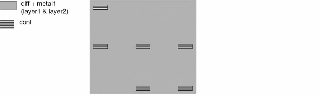
ruleContactDevice(
;( deviceName
 ( "VIABIGPOWER12"

;( layer1   purpose1   rectangles ) | nil
 ( diff     drawing    (-21.000 -21.000 21.000 21.000 ) )

;[( viaLayer   viaPurpose   rectangles )]
  ( cont       drawing      (  -2.400   -0.800    2.400     0.800   )
                            ( -19.000   17.400    -14.200   19.000  )
                            (  14.200   -19.000   19.000    -17.400 )
                            ( -19.000   -0.800    -14.200   0.800   )
                            (  -2.400   -19.000   2.400     -17.400 )
                            (  14.200   -0.800    19.000    0.800   )
  )

;[( layer2  purpose2   rectangles )]
  ( metal1   drawing    ( -21.000  -21.000  21.000  21.000 ) )
 )
) ; end of ruleContactDevice
Specifies the rule contact definition for a device called VIABIGPOWER12, which looks like the device shown in the figure below:
multipartPathTemplates
multipartPathTemplates( (t_mppTemplateName l_template) ; end of template … ) ;end of all multipartPathTemplates Rules ; l_template arguments ( l_masterPathArgs [l_offsetSubpathArgs...] [l_enclosureSubpathArgs...] [l_subrectangleArgs...] ) ; end of template argument lists ; l_masterPathArgs (txl_layer[n_width] [g_choppable] [t_endType] [n_beginExt] [n_endExt] [t_justification] [n_offset] [l_rodConnectivityArgs for master path] ) ;end of masterPathArgs list ; l_offsetSubpathArgs ( (txl_layer[n_width] [g_choppable] [n_sep] [t_justification] [n_beginOffset] [n_endOffset] [l_rodConnectivityArgs for offset subpath] ) ; end of first offset subpath list … ) ; end of all offset subpath lists ; l_enclosureSubpathArgs ( (txl_layer[n_enclosure] [g_choppable] [n_beginOffset] [n_endOffset] [l_rodConnectivityArgs for enclosure subpath] ) ; end of first enclosure subpath list … ) ; end of all enclosure subpath lists ; l_subRectangleArgs ( (txl_layer[n_width] [n_length] [g_choppable] [n_sep] [t_justification] [n_space] [n_beginOffset] [n_endOffset] [n_gap] [l_rodConnectivityArgs for subrectangles] [n_beginSegmentOffset] [n_endSegmentOffset] ) ; end of first subrectangle list … ) ; end of all subrectangle lists ; l_rodConnectivityArgs ([t_termIOType] [g_pin][tl_pinAccessDir][g_pinLabel][n_pinLabelHeight][txl_pinLabelLayer][t_pinLabelJust] [t_pinLabelFont][g_pinLabelDrafting][t_pinLabelOrient][t_pinLabelRefHandle] [l_pinLabelOffsetPoint] ) ; end of ROD Connectivity Argument list
Description
Defines a template or a series of templates that specify relative object design (ROD) multipart paths (MPPs). A multipart path is a single ROD object consisting of one or more parts at level zero in the hierarchy on the same or on different layers. An MPP template lets you create MPPs in the layout by using predefined values from the technology file. You can define any number of MPP templates in this section; each template must be identified by a unique template name (t_mppTemplateName).
Arguments
All other arguments for MPP templates in the multipartPathTemplates section have the same names, definitions, valid values, and default values as the arguments for the rodCreatPath function. For a detailed description of each argument, see the argument descriptions of the rodCreatePath function in Virtuoso Relative Object Design SKILL Reference.
Differences in the Syntax of multipartPathTemplates and rodCreatePath
The syntax for multipartPathTemplates is based on the syntax of the rodCreatePath function. For the arguments that multipartPathTemplates and rodCreatePath have in common, the argument definitions, valid values, and default values are identical.
The differences between the two are summarized below:
-
Arguments for
multipartPathTemplatesare positional; you must specify them in the sequence shown in the syntax formultipartPathTemplates. Arguments forrodCreatePathare keyword value pairs; you can specify them in any sequence. -
There is one additional argument in
multipartPathTemplates, t_mppTemplateName. -
For
multipartPathTemplates, all arguments other than t_mppTemplateName are specified as lists within the l_template list, including the connectivity arguments. -
For some arguments, the data type is more restricted for
multipartPathTemplatesthan it is forrodCreatePath. Specifically, you can enter either a character string or a symbol forrodCreatePatharguments with the data type S_; for the equivalentmultipartPathTemplatesarguments, you must enter a character string (the data type is t_ for text). -
multipartPathTemplatesdoes not contain the followingrodCreatePatharguments because the values of these arguments vary for each occurrence of an MPP within a cellview:
S_name and S_netName Enter values for these arguments in the ROD Name and Net Name fields in the Create ROD Multipart Path form.
S_termName The value of Net Name is used for terminal name.
l_pts Click in the layout cellview to specify the point list. -
multipartPathTemplatesdoes not contain therodCreatePatharguments listed below because these arguments represent an alternate way of specifying a point list for an MPP, and the point list varies for each occurrence of an MPP within a cellview:
dl_fromObj txf_size l_startHandle l_endHandle
For more information about the rodCreatePath function, its arguments, and default values, see rodCreatePath in Virtuoso Relative Object Design SKILL Reference.
Defining, Changing, and Deleting MPP Templates
You can define new MPP templates, change the values for existing template definitions, and delete existing template definitions.
-
You can define new MPPs for the
multipartPathTemplatessection by using any of the following three methods:-
Define an MPP in the Create Multipart Path form and save it as a template. To access the form, choose Create – Multipart Path in VLS XL.
For information about creating MPPs by using the graphical user interface, see Creating and Editing Multipart Paths in Virtuoso Layout Suite documentation. -
Dump the ASCII version of your technology file, edit it, and then reload it in Merge or Replace mode.
For information about loading the ASCII version of your technology file in Replace mode, see Replacing Existing Technology Data in a Technology Library in Virtuoso Technology Data User Guide. - To avoid the need to reload your technology file, use the techSetMPPTemplate function.
-
Define an MPP in the Create Multipart Path form and save it as a template. To access the form, choose Create – Multipart Path in VLS XL.
-
You can change the contents of an existing MPP template definition by editing the template in the Create Multipart Path form. You can also edit the
multipartPathTemplatessection in the ASCII version of your technology file and reload it in Merge or Replace mode. -
You can delete an MPP template definition from the
multipartPathTemplatessection of your technology library. After editing the ASCII version of your technology file, you can reload it in Replace mode. You can also choose to specify thetechSetMPPTemplatefunction as follows:techSetMPPTemplate( tfId "
wheretemplate_name" nil )tfIdis the technology file ID.
Specifying Positional Arguments
The arguments for defining an MPP template are positional. For example, if you want to specify values for only the first, fifth, and sixth arguments, you must specify nil or the required value for the second, third, and fourth arguments. You do not need to specify the arguments that appear after the sixth argument in the syntax.
The syntax is organized so that arguments you are most likely to specify are listed first and the arguments for which you probably want to use the default values are listed last. Most of the arguments have a system-assigned default value and are, therefore, optional. The only required argument is txl_layer for the master path and the subparts, if any.
Specifying Arguments as nil
Except for Boolean arguments (for which nil is a valid value), the value nil is a placeholder. For example, if you do not specify the n_width argument or specify n_width as nil, the default value, which is the minimum width for the layer as defined in the technology file, is used.
For MPP template definitions, nil means the following, depending on the type of argument:
-
For Boolean arguments,
nilis a valid value, so you cannot specifynilas a placeholder. The following are Boolean arguments:
g_choppable g_pin g_pinLabel g_pinLabelDrafting -
For non-Boolean arguments, specifying
nilcauses the default value, as it is defined for the argument in the rodCreatePath section in Virtuoso Relative Object Design SKILL Reference, to be used. Specifyingnilis equivalent to not specifying a value for the argument.
Specifying Template Arguments as Expressions
You can specify template arguments as expressions; the expressions are stored as part of the technology file. An expression must evaluate to a data type defined for the argument.
For example, you could specify the n_width argument by using the following expression:
2 * minWidth
If minWidth for the layer is defined as 1.5, the n_width argument is evaluated as 3.0. If minWidth is now updated to 1.2, n_width will be evaluated as 2.4 when you next access the template.
Example of an MPP Template Definition
The sample MPP template definition available at the end of this section is for a guard ring. Assuming that this template is already defined in your technology file, you can create the guard ring in a layout window by performing the following steps:
- Choose Create – Multipart Path.
-
From the MPP Template list, choose
guardring. -
Click the following five points in the canvas:
0:0 0:5 10:5 10:0.9 0.9:0.9
A guard ring, as shown in the figure below, is created:
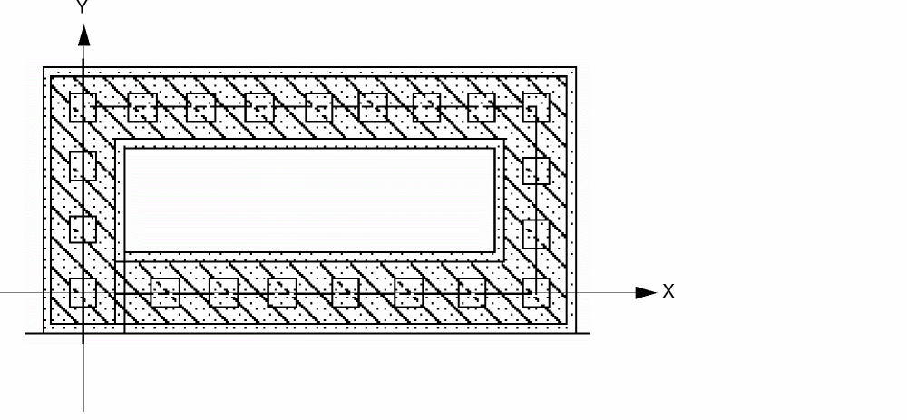
Sample MPP template definition for the guard ring shown in the figure above:
;********************************
; DEVICES
;********************************
devices(
multipartPathTemplates(
; ( name [masterPath] [offsetSubpaths] [encSubPaths] [subRects] )
;
;   masterPath:
;   (layer [width] [choppable] [endType] [beginExt] [endExt] [justify] [offset]
;   [connectivity])
;
;   offsetSubpaths:
;   (layer [width] [choppable] [separation] [justification] [begOffset] [endOffset]
;   [connectivity])
;
;   encSubPaths:
;   (layer [enclosure] [choppable] [begOffset] [endOffset] [connectivity])
;
;   subRects:
;   (layer [width] [length] [choppable] [separation] [justification] [space]
    [begOffset] [endOffset] [gap] [connectivity] [beginSegOffset] [endSegOffset])
;
;   connectivity:
;   ([I/O type] [pin] [accDir] [dispPinName] [height] [ layer]
;    [layer] [justification] [font] [textOptions] [orientation]
;    [refHandle] [offset])
;
( guardring
    ; master path:
    (
     ("diff" "drawing")      ; layer-purpose pair
  1.8     ; width
  nil     ; choppable
 )
 ; offset subpath (there is none)
 nil
    ; enclosure subpath:
    (
     ("metal1" "drawing")     ; layer-purpose pair
  0.2          ; enclosure
  t            ; choppable
  -0.2         ; begin offset
  0.2           ; end offset
 )
 ; set of subrectangles:
    (
     ("cont" "drawing"     ; layer-purpose pair
  nil          ; width
  nil          ; length
  t            ; choppable
  nil          ; separation
  nil          ; justification
  nil          ; space
  -0.6     ; begin offset
 )
  ) ; end guardring template
 ) ;multipartPathTemplates
) ;devices
waveguideTemplates
waveguideTemplates( (t_name(tx_masterLayer tx_masterPurpose) ['minWidthn_minWidth] ['minBendRadiusn_minBendRadius] ['modePropertiesl_modeProperties] ['maxTaperAnglef_maxTaperAngle] 'derivedShapeSpecs((tx_layer| (tx_layer tx_purpose) { 'type "enclosure" ['enclosuretn_enclosure] | 'type "offset" ['side "both" | "right" | "left"] ['innertn_inner] ['outertn_outer] } )... );derivedShapeSpecs );t_name
);waveguideTemplates
Description
(Virtuoso Photonics Option) Defines a template or a series of templates that specify waveguide objects. In Photonic Integrated Circuits, a waveguide is a 3D structure built as a vertical stack of shapes on neighboring layers. One of the layers forms the master, and the shapes on the other layers are relative to the master with some enclosure or offset.
For information about creating waveguides by using the graphical user interface, see Editing Composite Waveguides in Virtuoso Layout Suite documentation.
Arguments
|
Name of the template. The name must be unique within the |
|
|
The layer-purpose pair (LPP) on which the You can specify the LPP as a list of strings enclosed in double quotes and separated by a space:
Alternatively, you can specify a list of integers separated by a space: |
|
|
The mode properties of the waveguide object as a list in the following format:
|
|
|
The maximum angle that can be used when tapering a wave guide. A value of |
|
|
The object shape to be derived from the master shape. A derived shape definition list has the following format:
The tn_enclosure, tn_inner, and tn_outer values can be specified either as a string (in which case, they are interpreted and stored, without validation, as SKILL expressions) or as fixed numbers. For more information about this argument, see “Deriving Shapes”. |
|
Deriving Shapes
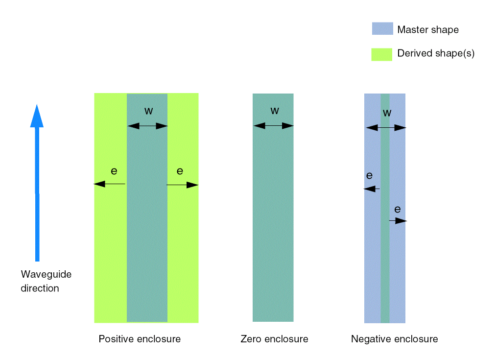
The following figure illustrates the three kinds of derived shapes.
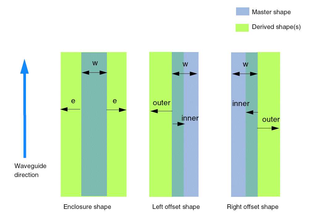
The following figure illustrates the direction in which the enclosure for enclosure shapes is applied. A positive number extends the enclosure outside the master shape. A zero enclosure results in a derived shape with the same dimensions as the master shape. A negative number makes the derived shape skinnier than the master shape.
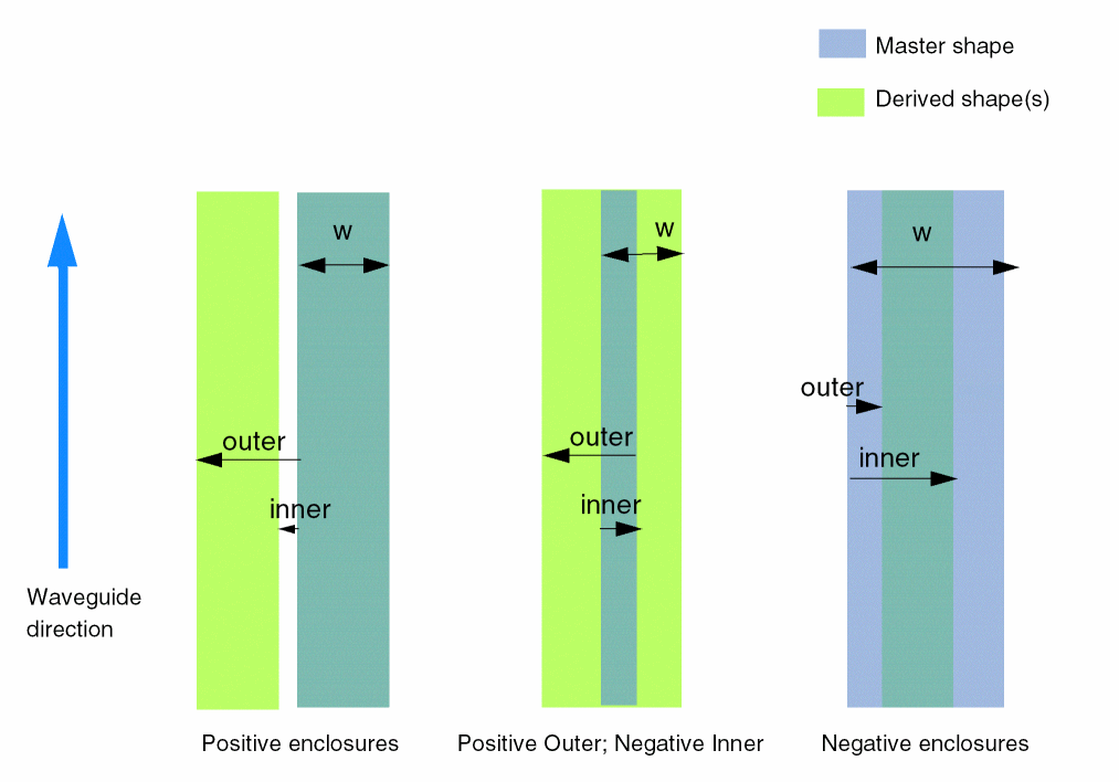
The following figures illustrates the direction in which the enclosure for offset shapes is applied. A positive number extends away from the edge of the master shape. A negative number is directed from the edge of the master shape into the master shape.
Example of a Waveguide Template Definition
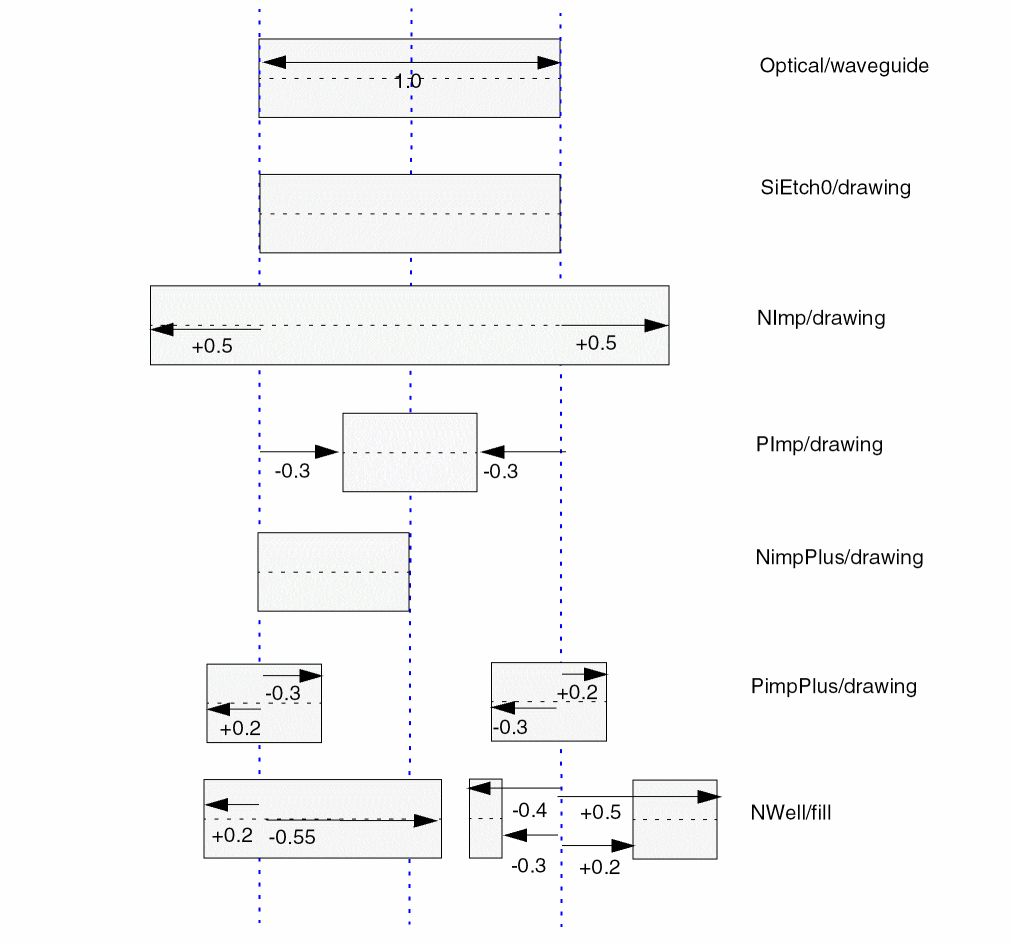
Let us consider the following sample waveguideTemplate definition.
waveguideTemplates( ("simpleWaveguide"("Optical""waveguide") 'minWidth 0.5
'minBendRadius 13.2
'modeProperties ('function "myFunc" 'names (( "mode1" 1) ("mode2" 2)))
'derivedShapeSpecs (
(("SiEtch0""drawing") 'type"enclosure"'enclosure 0.8) (("NImp""drawing") 'type"enclosure"'enclosure"0.5*w") (("PImp""drawing") 'type"enclosure"'enclosure -0.3 ) (("NimpPlus""drawing") 'type"offset"'side"left") (("PimpPlus""drawing") 'type"offset"'inner -0.3 'outer 0.2) (("NWell""fill") 'type"offset"'side"right"'inner"-0.4*w"'outer"-0.4*w + 0.1") (("NWell""fill") 'type"offset"'side"left"'inner -0.55 'outer 0.2) (("NWell""fill") 'type"offset"'side"right"'inner 0.2 'outer 0.5) ) ;simpleWaveguide
) ;waveguideTemplates
The following figure illustrates one example of such a waveguide. It shows a cross section, and the waveguide direction is assumed to be into the page, in the direction of the waveguide. As a result, the left side for a derived shape with the type offset is to the left of the master path. In this case, the master path width is 1.0 and all the expressions are calculated with w=1.0.
extractMOS
extractMOS(t_deviceName tx_recognitionLayer tx_gateLayer tx_sourceDrainLayer tx_bulkLayer[tx_modelName]
) ;extractMOS
Description
Defines the layers used to recognize and establish connections to a MOS transistor.
Arguments
Example
devices(
    extractMOS( "NMOS"  ngate  poly  oxide  substrate "lvn" )
    extractMOS( "PMOS"  pgate  poly  oxide  nwell     "lvp" )
)
extractRES
extractRES(tx_deviceName tx_recognitionLayer tx_termLayer[tx_modelName]
) ;extractRES
Description
Defines the layers used to recognize and establish connections to a resistor.
Arguments
Example
devices(
    extractRES( "polyR"  polyRes  poly  rp )
)
extractCAP
extractCAP(t_deviceName tx_recognitionLayer tx_plusLayer tx_minusLayer[tx_modelName]
) ;extractCAP
Description
Defines the layers used to recognize and establish connections to a capacitor.
Arguments
Example
devices(
    extractCAP( "polyC"  polyCap  poly1  poly2  cp )
)
extractDIODE
extractDIODE(t_deviceName tx_recognitionLayer tx_plusLayer tx_minusLayer[tx_modelName] )
Description
Defines the layers used to recognize and establish connections to a diode.
Arguments
Example
devices(
    extractDIODE( "nsubDiode"  ndiode  ndiff  substrate )
)
Return to top