8
Verifying CDF Operation
Testing the Component
Once you have completed the design of your component (all views and the Component Description Format are done), test the operation of the component’s CDF description before using the component in your design. The following is a procedure you might use.
Test Procedure
- Open an empty schematic and place instances of your symbol.
-
As you place the instances, use different parameter values.
Check the Add Instance form for confirmation that your parameter definitions and callbacks are working. Look for the following indications:- Parameters have the units you expected.
- Parameters have the defaults you expected.
- The correct parameters are at the top of the list of parameters. You should not have to keep scrolling down the form to edit important parameters.
- Parameters that are supposed to become noneditable do so when expected.
- Parameters that are not supposed to be displayed are not displayed as expected.
- Do your callbacks get called? First check. Do they stacktrace because you forgot to load them?
- Parameters whose values depend on other parameters update as you expect.
- Are your callbacks doing the range checking you set up?
- Can you enter bad parameter values?
-
After you place the instances, use Edit Properties (in the schematic editor) to look at the properties stored on the instances.
Look for the following: - Draw a minimal schematic and go to the simulator you will be using. Generate a netlist to make sure that your component netlists as you expect.
- Once you are satisfied with the schematic and simulation results, go to an empty layout and repeat the CDF tests to see the effect on your layout.
Virtuoso XL Layout Editor Procedure
If you are going to use the Virtuoso® XL Layout Editor (Virtuoso XL),
- Make a simple schematic with some examples of your component randomly wired to each other.
- Go through the Virtuoso XL design cycle.
- Check that you have set all the parameters that Virtuoso XL requires.
- Does Virtuoso XL place the layouts you expect with appropriate connectivity?
LVS Procedure
If you are using Layout Versus Schematic (LVS),
- Create a simple schematic and layout with few instances.
- Run extraction and LVS.
-
Make sure the LVS netlist is correct.
This also gives you a chance to check out the LVS rules in a controlled experiment using just one device.
Making Changes
If you find a problem or change the design, follow these guidelines:
- If problems occur during testing, fix the views or CDF and retest.
-
For the parameter type
netSet, it is mandatory to set the attribute storeDefault to yes. -
If the problem or change occurs after you have placed multiple instances of the component, consider the following:
- You might need to change just the user interface, such as the order of the parameters or which parameters are displayed in the form or label display. When you make a change, it is inherited by all existing instances.
- If you change the default value of a parameter with the attribute storeDefault = no, it is inherited by all existing instances. (Use the Window – Redraw command to see the changes reflected in the current window.)
- If you change the default value of a parameter with storeDefault = yes, changing the default value does not update the existing instance, because the value was saved as a property on each instance.
- If you change a callback that sets the value of one parameter based on an equation involving another parameter, changing the default value does not update the existing instances. You must also trigger the callback again, for each instance.
In the last two cases, you can update existing instances using the Cadence Analog Design Environment – Design Variables – Update command. This command updates the default values and triggers all of the callbacks of all of the instances in the current window. The Update command has the following limitations:
Finishing the NFET Example
In the last part of the NFET example you can see visible changes in the cell layout and form displays as a result of changing the CDF data.
Varying the Layout
Once you enter all the CDF information for the NFET into the system, you can display the transistor layout. The Pcell layout (stored in view layout) might look as shown in the following figure:
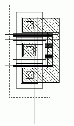
This is a Pcell with the following parameters:
The NFET looks like the following with different parameter combinations:
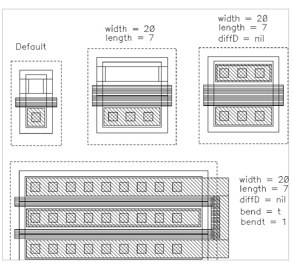
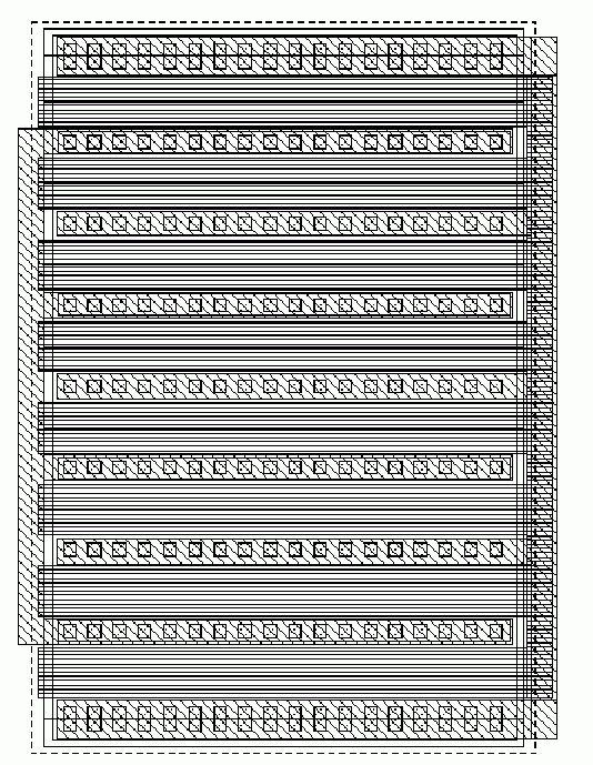
In addition, you need the fixed layout for the power applications. This might be stored under view layout.pwr, have a gate width of 880 micrometers and length of 12 micrometers, and look like this:
Changing Parameters
Now try to use the NFET in a design.
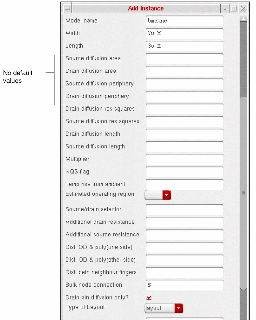
When you first use the Add Instance form, some fields are dimmed.
The first time you open the Add Instance form for your component, it shows all default values. Some default values are not defined. At this point, you might want to go back to the Edit CDF form and add the appropriate default values.
Notice, however, that you cannot enter values in the fields with dim names. If you use the CDF description to set a parameter to be displayed, but not editable, the parameter field is not editable on the Add Instance form.
The type of layout is cyclic, as you specified. The width and length are prompted for only once, as a string with units of length.
As you place instances of the NFET, you never change the value for the bulk node connection. Therefore, you might use the Edit CDF form to move that parameter down in the list of parameters until it is below other parameters that you do change.
-
Change the Type of Layout cyclic button. The Add Instance form updates as follows:
You can see the form modify itself to show the new fields, indicating that the callbacks are working.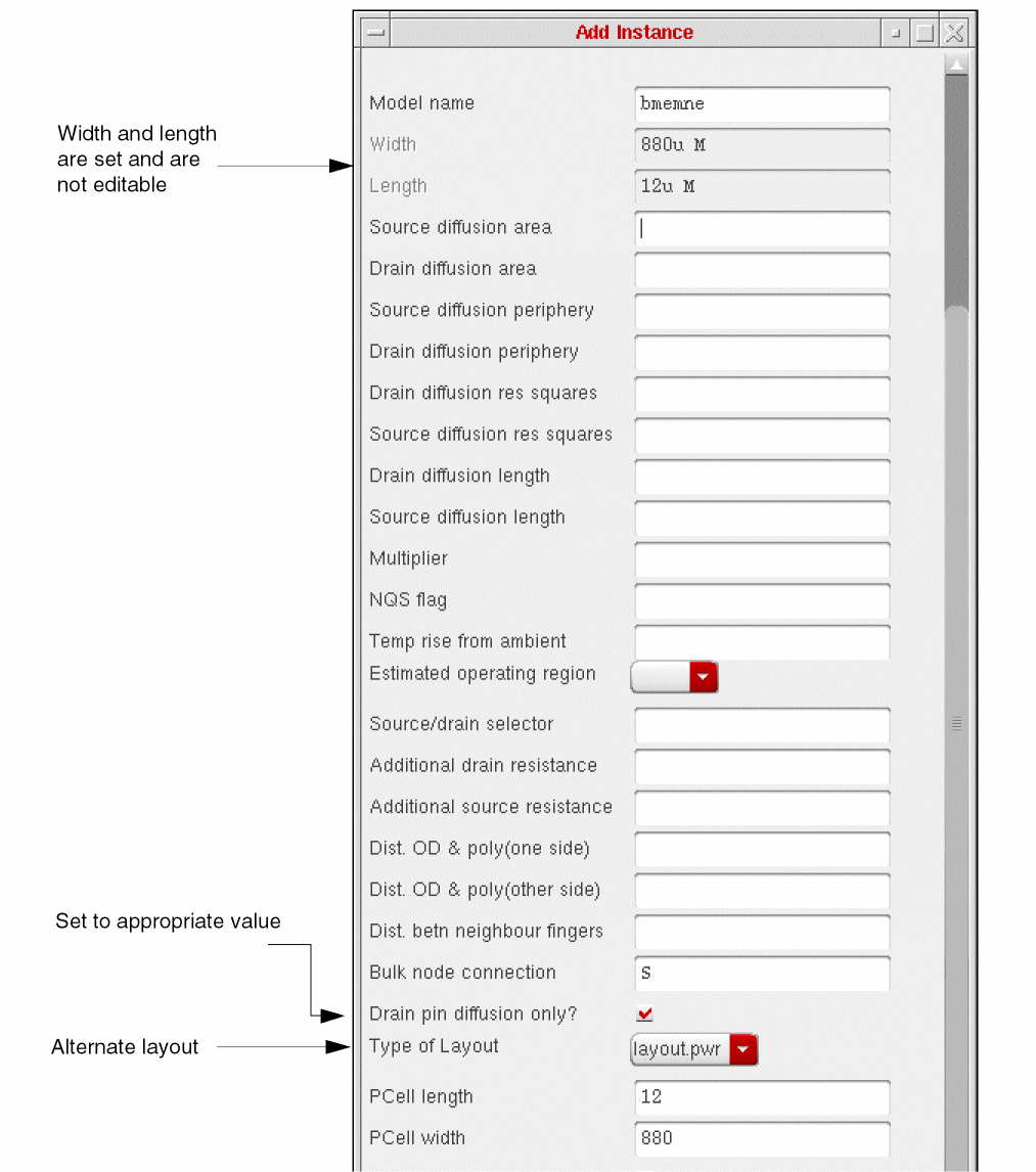
At this point you still cannot see if the Pcell parameters are being set properly. - Use the Edit – Properties – Object command on a few examples to verify the operation of the Pcell parameters in the CDF description.
-
Using the Edit Object Properties form, create an instance with width set to
30u, length set to10u, the default layout, and a drain diffusion pin.
The CDF Parameter fields in the Edit Object Properties form should look like this:
These values indicate that the callbacks used to generate Pcell parameter values worked correctly. If you have a different result, check the callbacks in the CDF description.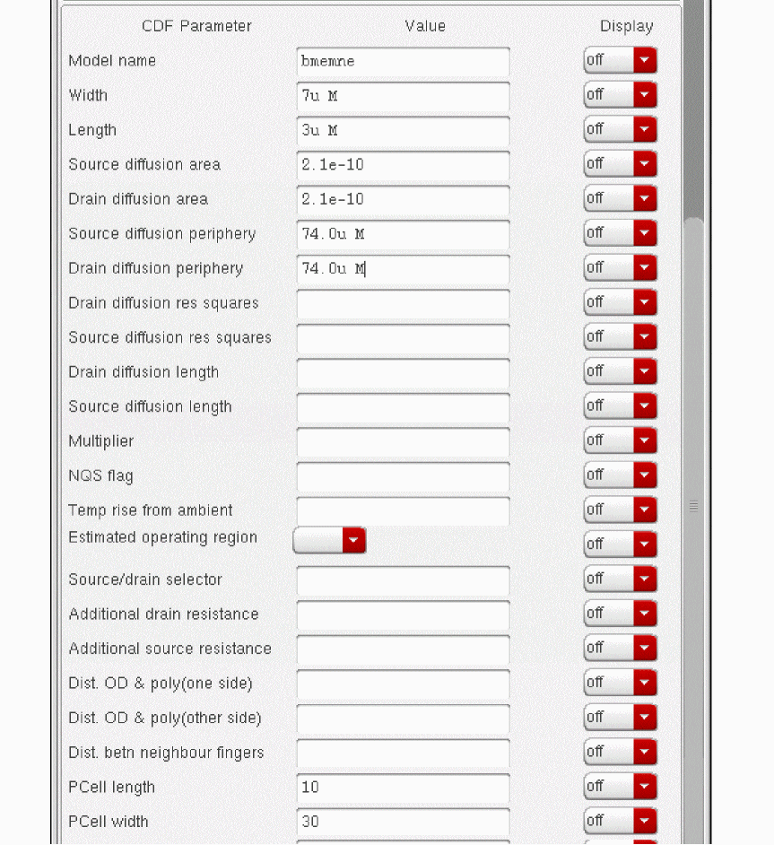
-
Create an instance of the NFET with width set to
130u, length set to3u(default), the default layout, and no drain diffusion pin (required).
The Edit Object Properties form should look like the following:
Both of the length parameters are default values, so no property is saved.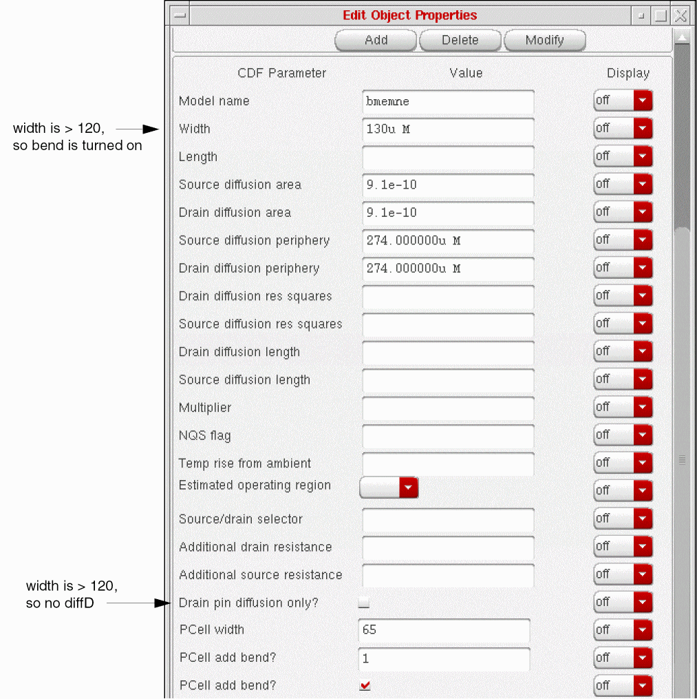
-
Create an instance with maskLayoutViewName as
layout.pwr.
You see the following:
All the callbacks are triggered, as expected.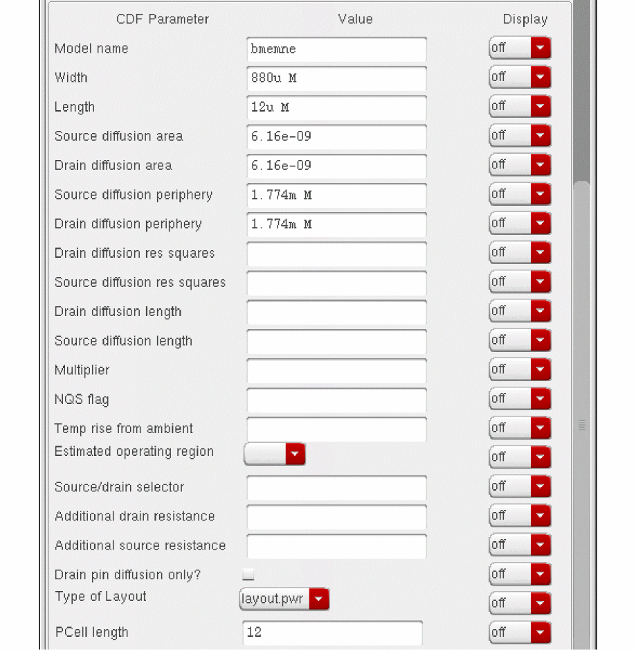
Return to top