1
Modeling for Direct Simulation
Cadence strongly recommends that you use the modeling practices described in this document. Cadence is committed to these modeling practices, and these practices are fully supported by the Virtuoso Analog Design Environment, the Spectre Circuit Simulator, and the Spectre interface.
By employing the direct modeling practices described in this document, you can use different types of models without making any design changes. For example, you can model an npn device as
- a simple simulator model statement,
-
a simple
subcktdefinition, -
an advanced
subcktdefinition, or - a behavioral definition.
Neither the design nor the component description format (CDF) of the npn component in analogLib needs to change. You can change the model complexity without design or CDF edits.
Modeling Strategies
This document gives you information about the implementation and advisability of the following modeling strategies:
- Simple Device Models describes how to use the simplest device models which do not contain expressions, user-defined parameters, or instance parameters.
- Built-In Geometric Models describes how to specify parameters in addition to those included in simple device models. This method is convenient when the unmodified instance parameters provided by the simulator are adequate, such as when the simulator performs geometric scaling internally.
- External Models describes how to define models that are based on the models provided by the simulator but which have slightly different behavior or interface. The modifications are implemented outside the simulator, as opposed to internally, and defined in a file.
- Standard Model Binning describes how to select a different model for each range of device geometries.
- Custom Model Binning describes how to select a different model for different ranges of certain parameters, but in contrast to standard binning, this capability is not built into the model. Instead, it is a general simulator capability.
- Process Modeling describes how to include, or not include, process and geometry effects in your simulation.
- Corners Modeling describes how to create one library that places the worst, typical, and best cases in one model file.
- Monte Carlo Modeling describes how to use statistical quantities in your models.
- Package Modeling points to a discussion of package modeling in the Spectre Circuit Simulator and Accelerated Parallel Simulator RF Analysis User Guide.
- Behavioral Modeling describes how to use behavioral models to abstract parts of a design to shorten the simulation time.
- Miscellaneous Modeling Techniques summarizes several other modeling techniques used in analog simulation. The usefulness of each technique is discussed, as is the degree of support for each technique available from Cadence tools.
- Libraries explains how devices are created for simulation in a Cadence library.
Licensing Requirements
For information about licensing in the Virtuoso Studio Design Environment, see Virtuoso Software Licensing and Configuration Guide.
Simple Device Models
In analog simulation, components frequently reference models. For example, a bjt component requires both an instance and a definition of the model it references. The instances and the model definitions can be complex or simple.
This section describes the use of the simplest device models. With simple device models, no expressions, no user-defined parameters, and no instance parameters are used.
An example of a simple device model is the instance Q25 in the schematic view of the opamp cell from the aExamples library which is shown in Figure 1-1.
Figure 1-1 opamp Cell from the aExamples Library Showing Q25
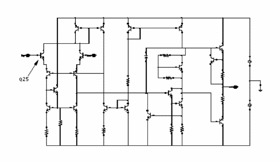
You can find the aExamples library in the directory tools/dfII/samples/artist in your Cadence installation directory.
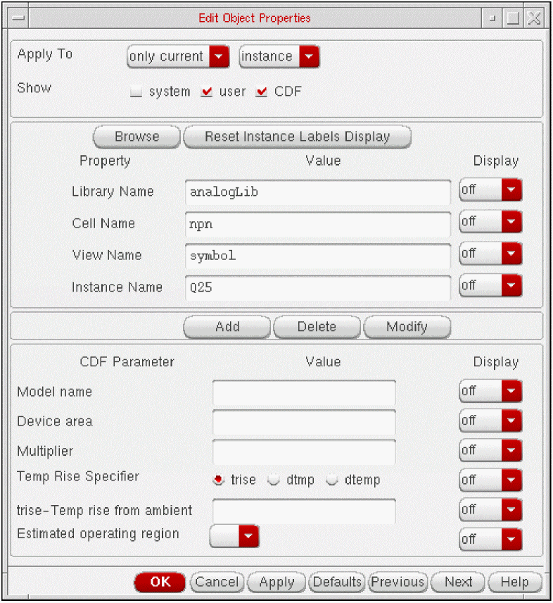
In the Edit Object Properties form shown in the following figure, the model parameter, Model name is for the instance Q25 and is npn. This makes this instance a reference to the npn model.
Figure 1-2 Edit Object Properties Form for Instance Q25 of the aExamples opamp
The netlist lines in Figure 1-3 show the Spectre syntax for this device instance along with the model npn it references shown in Figure 1-4. The model defines both the device type (bjt) and the parameters associated with the device.
The model npn is included from the file tools/dfII/samples/artist/models/spectre/models.scs.
The opamp cell in Figure 1-1 is used by the lowpass schematic cell view in the same library. When you simulate this cell view in the Virtuoso Analog Design Environment, you specify models.scs as the model file by typing this filename in the Setup Model Libraries form.
Figure 1-3 File: lowpass.scs for Simple Device Models
simulator lang=spectre
...
include "models.scs"
...
Q25 (net39 inp net80) npn
...
Figure 1-4 File: bipolar.scs for Simple Device Models
...
model npn bjt type=npn is=3.26E-16 va=60 bf=100 \
br=6 nc=2 ikr=100m rc=1 vje=0.7 \
cjc=1e-12 fc=0.5 cje=0.7p \
tr=200e-12 tf=25e-12 itf=0.03 vtf=7 xtf=2
...
Built-In Geometric Models
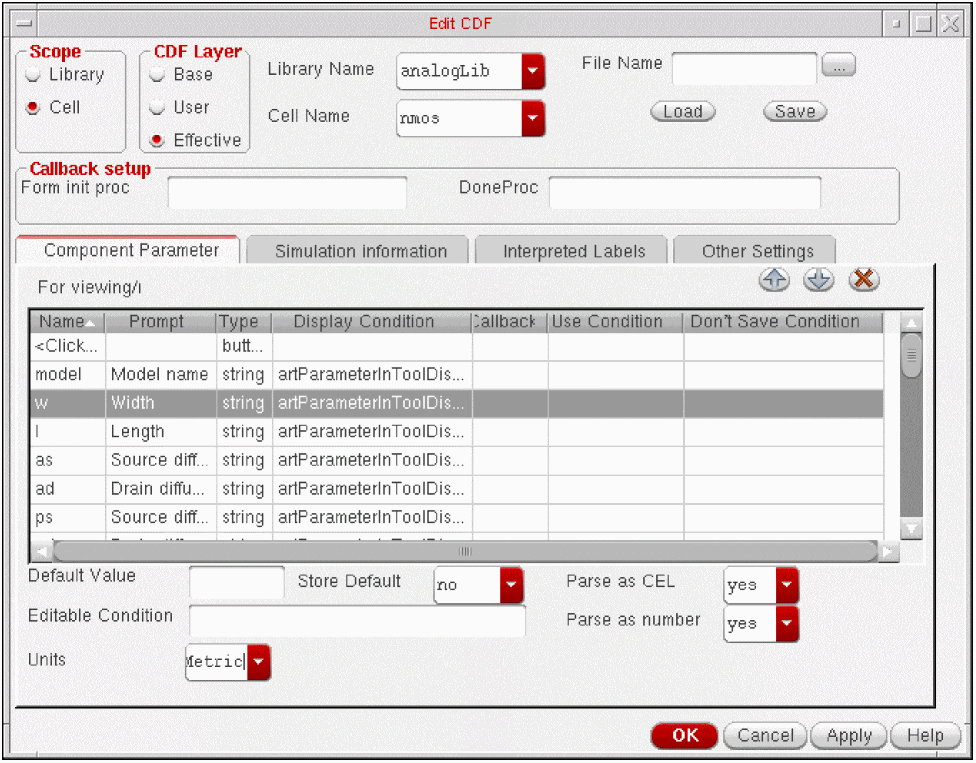
For most device primitives, you can specify additional parameters besides those included in the model. For example, with the l and w parameters, you can change the size of specific instances of Spectre MOS devices that are otherwise identical and described by a single model statement. This method is convenient when the unmodified instance parameters provided by the simulator are adequate for your simulation needs, such as when the simulator performs geometric scaling internally.
In the l and w, to the list of instance parameters in the simulator information section for each simulator of interest. For the nmos cell of the analogLib library, you define the l and w parameters in the CDF with the prompts Length and Width respectively. These parameters are referenced in the instParameters section of the Edit Simulation Information form.
Figure 1-5 Edit CDF Form for the nmos Cell
The instances M14 and M15 in the schematic view of the foldedCascode cell in the aExamples library, shown in Figure 1-6, demonstrate this technique. Both instances have identical values for l and w. The instances M2 and M4 also use this technique, and although these instances differ in size, both reference model nmos24 as shown in Figure 1-7.
Figure 1-6 foldedCascode Cell From the aExamples Library
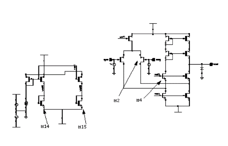
Figure 1-7 File: foldedCascode.scs for Built-In Geometric Models
simulator lang=spectre
...
include "basicMos.scs"
...
M2 (2 1 0 0) nmos24 l=3u w=40u
...
M4 (2 1 0 0) nmos24 l=1.8u w=20u
...
The basicMos.scs file in Figure 1-8 is selected as the model file on the
Figure 1-8 File: basicMos.scs for Built-In Geometric Models
...
model nmos24 mos2 type=n vto = 0.775 tox = 400e-10 nsub = 8e+15
+ xj = 0.15u ld = 0.20u uo = 650 ucrit = 0.62e+5 uexp = 0.125
+ vmax = 5.1e+4 neff = 4.0 delta = 1.4 rsh = 36 cgso = 1.95e-10
+ cgdo = 1.95e-10 cj = 195u cjsw = 500p mj = 0.76 mjsw = 0.30
+ pb = 0.8
...
After simulation, the operating-point results for the instance appear in the Results Browser as shown in Figure 1-9.
Figure 1-9 Operating Points for the Built-In Geometric Models Example
External Models
In some cases, specifying different parameter values for the instances of built-in models, as is shown in the previous example, Built-In Geometric Models, is not a satisfactory solution. External modeling might be a preferred procedure.
With external modeling, you define models that are based on the models provided by the simulator but that have slightly different behavior or interfaces. The modifications are implemented outside the simulator, as opposed to internally, and are defined in a file that is normally provided by the foundry developer. This file might contain parameter definitions, function definitions, and an extra layer of computation, as well as the modified model.
You can also further modify the behavior of an individual device with your own instance parameters. For example, the length and width are often user-specified for bipolar devices, but these parameters might not be available in a particular simulator. The following features or effects might be modeled in an externally created model:
You can accomplish external modeling by making instance parameter and model parameter values functions of the quantity of interest, such as geometry. This approach is available within the
Compare the netlist in Figure 1-10 to the example shown in Figure 1-7 that also utilizes the M2 and M4 instances in the foldedCascode circuit shown in Figure 1-6. In both examples, the M2 and M4 instances reference the same model nmos24 but specify instance values for the l and w parameters.
The two examples differ in the choice of the model file. The external modeling example uses externalMos.scs in Figure 1-11 instead of basicMos.scs shown in Figure 1-8. Without any changes to the foldedCascode schematic in Figure 1-6, a more powerful modeling approach is used by specifying a different filename. For external modeling, the file in Figure 1-10 is the netlist created by the Virtuoso Analog Design Environment:
Figure 1-10 File: foldedCascode.scs for External Models
// Using direct netlister
simulator lang=spectre
...
include "externalMos.scs"
...
M2 (2 1 0 0) nmos24 l=3u w=40u
...
M4 (2 1 0 0) nmos24 l=1.8u w=20u
...
This example demonstrates modeling of geometry with process effects. The externalMos.scs model file in Figure 1-11 is located in the samples directory tools/dfII/samples/artist/models/spectre.
In the externalMos.scs model file, the variables mos24LengthOffset and mos24WidthOffset, as well as the functions mos24LengthCorrection and mos24WidthCorrection, are defined for the nmos24 model. The variable values nmos24LengthOffset and nmos24WidthOffset (.1μ, .015μ) are called process parameters. These process parameters are used in both a function and an algebraic expression where they are combined with the user-defined instance parameters l and w to determine the effective length and width. The l and w parameters of instance _mos in the nmos24 and pmos24 inline subckt definitions use the functions mos24LengthCorrection and mos24WidthCorrection to determine their values.
The externalMos.scs file shown in Figure 1-11 includes an inline subckt definition which replaces the nmos24 model card of the basicMos.scs file shown in Figure 1-8. The inline subckt contains a single instance of a device as well as a model definition. The terminals are identical to those of the Spectre mos2 model.
The parameters l and w for the foldedCascode example in Figure 1-10 are also defined in the inline subckt definition of Figure 1-11. The inline subckt definition transparently replaces the model statement from Figure 1-10. Inside the inline subckt definition, the length and width of the instance are replaced with corrected values.
The example in Figure 1-11 shows alteration of the instance parameters. Of course, the model parameters can be altered.
Figure 1-11 File: externalMos.scs for External Models
simulator lang=spectre
parameters mos24LengthOffset=.1u mos24WidthOffset=.015u
real mos24WidthCorrection( real w, real offset ) {
return w + offset
}
real mos24LengthCorrection( real l, real offset ) {
return l + offset
}
inline subckt nmos24 (d g s b)
parameters w=1 l=1
nmos24 (d g s b) _mos l=mos24LengthCorrection( l, mos24LengthOffset )
+ w=mos24WidthCorrection( w, mos24WidthOffset )
model _mos mos2 type=n vto = 0.775 tox = 400e-10 nsub = 8e+15
+ xj = 0.15u ld = 0.20u uo = 650 ucrit = 0.62e+5 uexp = 0.125
+ vmax = 5.1e+4 neff = 4.0 delta = 1.4 rsh = 36 cgso = 1.95e-10
+ cgdo = 1.95e-10 cj = 195u cjsw = 500p mj = 0.76 mjsw = 0.30
+ pb = 0.8
ends
inline subckt pmos24 (d g s b)
parameters w=1 l=1
pmos24 (d g s b) _mos l=mos24LengthCorrection( l, mos24LengthOffset )
+ w=mos24WidthCorrection( w, mos24WidthOffset )
model _mos mos2 type=p vto = -0.75 tox = 400e-10 nsub = 6e+15
+ xj = 0.05u ld = 0.20u uo = 255 ucrit = 0.86e+5 uexp = 0.29
+ vm = 3.0e+4 neff = 2.65 delta = 1.0 rsh = 101 cgso = 1.90e-10
+ cgdo = 1.90e-10 cj = 250u cjsw = 350p mj = 0.535 mjsw = 0.34
+ pb = 0.8
ends
nmos24LengthOffset and mos24WidthOffset before you reference them.
An inline subckt definition is used instead of a subckt definition to make the simulation results appear similar to mos2 results. With inline subcircuits, no extra hierarchy is introduced by the use of subcircuits. The inline subckt contains a single instance whose instance name is identical to the name of the inline subckt, nmos24.
After simulation, you can display the operating points for M2 in the Results Browser. Compare the operating-point results with those shown in Figure 1-9. The operating-point names are identical to those of the model card although the values might differ because of the offsets of width and length in externalMos.scs.
For more information about inline subcircuits, see the Spectre Circuit Simulator Reference.
Standard Model Binning
When you specify the stdbinMos.scs file for the foldedCascode example shown in Figure 1-12 on the M2 and M4. This modeling style is again different from that in the previous two examples in Figure 1-7 and Figure 1-10 while the schematic shown in Figure 1-6 is the same.
The resulting netlist is shown below:
Figure 1-12 File: foldedCascode.scs for Standard Model Binning
// Using direct netlister
simulator lang=spectre
...
include "stdbinMos.scs"
...
M2 (2 1 0 0) nmos24 l=3u w=40u
...
M4 (2 1 0 0) nmos24 l=1.8u w=20u
...
The following is a section of the sample model file:
Figure 1-13 File: stdbinMos.scs for Standard Model Binning
simulator lang=spectre
...
model nmos24 mos2 {
1: type=n vto = 0.775 tox = 400e-10 nsub = 8e+15
+ xj = 0.15u ld = 0.20u uo = 650 ucrit = 0.62e+5 uexp = 0.125
+ vmax = 5.1e+4 neff = 4.0 delta = 1.4 rsh = 36 cgso = 1.95e-10
+ cgdo = 1.95e-10 cj = 195u cjsw = 500p mj = 0.76 mjsw = 0.30
+ pb = 0.8 lmin=0.1u lmax=2u wmin=1u wmax=30u
2: type=n vto = 0.775 tox = 400e-10 nsub = 8e+15
+ xj = 0.15u ld = 0.20u uo = 650 ucrit = 0.62e+5 uexp = 0.125
+ vmax = 5.1e+4 neff = 4.0 delta = 1.4 rsh = 36 cgso = 1.95e-10
+ cgdo = 1.95e-10 cj = 195u cjsw = 500p mj = 0.76 mjsw = 0.30
+ pb = 0.8 lmin=2u lmax=10u wmin=30u wmax=100u
}
...
Custom Model Binning
As is the case with standard binning, a different model is selected for different ranges of certain parameters, but in contrast to standard binning, the custom binning capability is not built into the model. Instead, it is a general simulator capability.
In this example, the appropriate model is selected by the simulator for each device or subcircuit instance based on the values of the subcircuit parameters for the area of that instance. The model selection can be based on any parameter, not just on geometry parameters.
Unlike standard binning, which is limited to the l and w parameters for mos devices, custom binning can be used for any parameter or design variable of any device type, including bipolar devices. In Spectre, custom binning is achieved using the structural if statement, as shown in cstbinMos.scs in Figure 1-15, and the conditional expressions used in the if statements can reference any netlist parameter, subcircuit parameter, or design variable.
The cstbinMos.scs file in Figure 1-15 is located in the samples directory tools/dfII/samples/artist/models/spectre.
When you specify the cstbinMos.scs model file on the model setup form for the foldedCascode example shown in Figure 1-14, different model sections are again used for instances M2 and M4. The resulting netlist is shown in Figure 1-14:
Figure 1-14 File: foldedCascode.scs for Custom Model Binning
// Using direct netlister
simulator lang=spectre
...
include "cstbinMos.scs"
...
M2 (2 1 0 0) nmos24 l=3u w=40u
...
M4 (2 1 0 0) nmos24 l=1.8u w=20u
...
Figure 1-15 is a section of the sample model file.
Figure 1-15 File: cstbinMos.scs for Custom Model Binning
simulator lang=spectre
inline subckt nmos24 (d g s b)
parameters l=1u w=1u area=l*w
if (area < 4e-12) {
nmos24 (d g s b) small l=l w=w
} else {
nmos24 (d g s b) large l=l w=w
}
model small mos2 type=n vto = 0.775 tox = 400e-10 nsub = 8e+15
+ xj = 0.15u ld = 0.20u uo = 650 ucrit = 0.62e+5 uexp = 0.125
+ vmax = 5.1e+4 neff = 4.0 delta = 1.4 rsh = 36 cgso = 1.95e-10
+ cgdo = 1.95e-10 cj = 195u cjsw = 500p mj = 0.76 mjsw = 0.30
+ pb = 0.8
model large mos2 type=n vto = 0.775 tox = 400e-10 nsub = 8e+15
+ xj = 0.15u ld = 0.20u uo = 650 ucrit = 0.62e+5 uexp = 0.125
+ vmax = 5.1e+4 neff = 4.0 delta = 1.4 rsh = 36 cgso = 1.95e-10
+ cgdo = 1.95e-10 cj = 195u cjsw = 500p mj = 0.76 mjsw = 0.30
+ pb = 0.8 lmin=2u lmax=10u wmin=30u wmax=100u
ends nmos24
inline subckt pmos24 (d g s b)
parameters l=1u w=1u area=l*w
if (area < 4e-12) {
_mos (d g s b) small l=l w=w
} else {
_mos (d g s b) large l=l w=w
}
model small mos2 type=p vto = 0.775 tox = 400e-10 nsub = 8e+15
+ xj = 0.15u ld = 0.20u uo = 650 ucrit = 0.62e+5 uexp = 0.125
+ vmax = 5.1e+4 neff = 4.0 delta = 1.4 rsh = 36 cgso = 1.95e-10
+ cgdo = 1.95e-10 cj = 195u cjsw = 500p mj = 0.76 mjsw = 0.30
+ pb = 0.8
model large mos2 type=p vto = 0.775 tox = 400e-10 nsub = 8e+15
+ xj = 0.15u ld = 0.20u uo = 650 ucrit = 0.62e+5 uexp = 0.125
+ vmax = 5.1e+4 neff = 4.0 delta = 1.4 rsh = 36 cgso = 1.95e-10
+ cgdo = 1.95e-10 cj = 195u cjsw = 500p mj = 0.76 mjsw = 0.30
+ pb = 0.8 lmin=2u lmax=10u wmin=30u wmax=100u
ends pmos24
In this example, model binning is performed for MOS devices within the inline subcircuit definition. The devices M2 and M4 in the foldedCascode example in Figure 1-14 reference the same model nmos24. The values of the l and w parameters, which are passed from the M2 and M4 instances, determine the appropriate model definition. No instance or model names change in the result files.
Process Modeling
Successful IC design requires accurate modeling of the fabrication process. Many of the techniques described in previous sections are used in the netlist below. This section shows a Spectre simulator example of a complete process modeling approach. The example shows you how to create a netlist that lets you include, or not include (plain simulation), process and geometry effects in your simulation.
-
To include process and geometry effects in your simulation, include the
Process.scsfile in thediffamp.cktnetlist instead of thePlain.hfile. -
To perform a plain simulation which does not model the process and geometry effects, include the
Plain.hfile in thediffamp.cktnetlist instead of theProcess.scsfile.
The diffamp schematic cell view in Figure 1-16 from the aExamples library is a simple differential amplifier with two resistors and two npn bipolar transistors. The resistor and bipolar models are defined in the ProcessSimple.scs file. Both process and geometry effects are also modeled in this file.
When you include the Process.scs file shown in Figure 1-19 in the netlist, you specify geometric parameters to model bjt and resistor devices. Certain non-ideal process effects are also modeled in this file.
The Plain.scs file shown in Figure 1-20 is not used in this example, but it gives you an interface in which the parameters that you specify are the electrical parameters used by the simulator.
Figure 1-16 diffamp Schematic from the aExamples Library
Figure 1-17 File: diffamp.scs for Process Modeling
// A differential amplifier, biased with a 1mA current source
simulator lang=spectre
include "ProcessSimple.scs"
include "Process.scs"
E1 (1 0) vsource dc=12
// Pullup resistors, 4k ohms nominal
R1 (1 2) RPLR Rnom=4k WB=5 // 5 units wide, model calcs required length
R2 (1 3) RPLR Rnom=4k WB=10 // 10 units wide, model calcs required length
// The input pair
TNSA1 (2 4 5 0) TNSA WE=10 LE=10
TNSA2 (3 4 5 0) TNSA WE=10 LE=10
// No differential input voltage, both inputs tied to same source
E4 (4 0) vsource dc=5
// current source biasing
J5 (5 0) isource dc=1m
dcop dc
Figure 1-18 File: ProcessSimple.scs for Process Modeling
simulator lang=spectre
// Define process parameters, including mismatch effects
parameters RSHSP=200 RSHPI=5k // sheet resistance, pinched sheet res
+ SPDW=0 SNDW=0 // etching variation from ideal
+ XISN=1 XBFN=1 XRSP=1 // device “mismatch” parameters
+ XISNafac=100m XISNbfac=1m // IS scaling factors for mismatch eqns
+ XBFNafac=100m XBFNbfac=1m // BF “ “ “ “ “
+ XRSPafac=100m XRSPbfac=1m // RS “ “ “ “ “
+ RSHSPnom=200 RSHPInom=5k // sheet resistance nominal values
+ FRSHPI=RSHPI/RSHPInom // ratio of PI sheet res to nominal
// Define "simple" bipolar and resistor devices...
// Define a "base" TNSA subckt i.e
// Define a simple "TNSA" bipolar transistor subcircuit, with model // card
inline subckt TNSA_B (C B E S)
parameters MULT=1 IS=1e-15 BF=100
model modX bjt type=npn is=IS bf=BF // a model card
TNSA_B (C B E S) modX m=MULT // "inline" device instance
ends TNSA_B
// Define a "base" resistor
// A simple "RPLR" resistor subcircuit
inline subckt RPLR_B (A B)
parameters R MULT=1
RPLR_B (A B) resistor r=R m=MULT // "inline" device
ends RPLR_B
// Define process/geometry dependent bipolar and resistor devices..
// Define a "geometrical/process" TNSA subckt
// Define BJT subcircuit, with process and geometry effects modeled
// Bipolar model parameters IS and BF are functions of the
// effective emitter area/perimeter taking process factors
// (e.g non-ideal etching) into account
inline subckt TNSA_PR (C B E S)
parameters WE LE MULT=1 dIS=0 dBF=0
+ WEA=WE+SNDW // effective or "Actual" emitter width
+ LEA=LE+SNDW // effective or "Actual" emitter length
+ AE=WEA*LEA // effective emitter area
+ IS=1e-18*FRSHPI*AE*(1+(XISNafac/sqrt(AE)+XISNbfac)
+ *(dIS/2+XISN-1)/sqrt(MULT))
+ BF=100*FRSHPI*(1+(XBFNafac/sqrt(AE)+XBFNbfac)
+ *(dBF/2+XBFN-1)/sqrt(MULT))
TNSA_PR (C B E S) TNSA_B IS=IS BF=BF MULT=MULT // "inline"
ends TNSA_PR
// Define a "geometrical/process" RPLR resistor subckt
// Resistance is function of effective device geometry, taking
// process factors (e.g non-ideal etching) into account
inline subckt RPLR_PR (A B)
parameters Rnom WB MULT=1 dR=0
+ LB=Rnom*WB/RSHSPnom
+ AB=LB*(WB+SPDW)
RPLR_PR (A B) RPLR_B R=RSHSP*LB/(WB+SPDW)*(1+(XRSPafac/sqrt(AB)+XRSPbfac)
+ *(dR/2+XRSP-1)/sqrt(MULT))
ends RPLR_PR
Figure 1-19 File: Process.scs for Process Modeling
// Provides the designer with "geometrical" device interface
simulator lang=spectre
// Call to the geometrical TNSA model
inline subckt TNSA (C B E S)
parameters WE=1u LE=1u MULT=1 dIS=0 dBF=0
TNSA (C B E S) TNSA_PR WE=WE LE=LE \
MULT=MULT dIS=dIS dBF=dBF // call TNSA_PR
ends TNSA
// Call to the geometrical RPLR model
inline subckt RPLR (A B)
parameters Rnom=1 WB=10u MULT=1 dR=0
RPLR (A B) RPLR_PR Rnom=Rnom WB=WB \
MULT=MULT dR=dR // call RPLR_PR
ends RPLR
Figure 1-20 File: Plain.scs for Process Modeling
//
// Provides designer with "plain" device interface (i.e.
// no geometrical or process modeling)
simulator lang=spectre
// Plain TNSA, no geometrical or process modeling
inline subckt TNSA (C B E S)
parameters MULT=1 IS=1e-15 BF=100
TNSA (C B E S) TNSA_B IS=IS BF=BF MULT=MULT // call TNSA_B
ends TNSA
// Plain RPLR no geometrical or process modeling
inline subckt RPLR (A B)
parameters R=1 MULT=1
RPLR (A B) RPLR_B R=R MULT=MULT
ends RPLR
The number of process variables and functions might be large for realistic processes and designs. Using many expressions, like increasing design size, can slow the simulation, and tasks such as reading in user-defined functions and process variables might have an impact on performance.
Corners Modeling
You can create one library that places the worst, typical, and best cases in one models file. The foldedCascode schematic view shown in Figure 1-6 in the aExamples library is used as an example of this practice. The cornersMos.scs models file contains worst, typical, and best case models. The
The method shown below is the preferred approach. You place all the models in one file and then include the models you want to use.
The netlist created for this design from the foldedCascode.scs in Figure 1-21.
Figure 1-21 File: foldedCascode.scs for Corners Modeling
*
simulator lang=spectre
...
include "cornersMos.scs" section=FCS
...
File: cornersMos.scs
library vti_2u
section TNTP
simulator lang=spice
* VTI-derived Level=2 nominal model
.model nmos24 nmos level=2 vto = 0.775 tox = 400e-10 nsub = 8e+15 xj = 0.15U ld = 0.20U u0 = 650 ucrit = 0.62e+5 uexp = 0.125 vmax = 5.1e+4 neff = 4.0 delta = 1.4 rsh = 36 cgso = 1.95e-10 cgdo = 1.95e-10 cj = 195U cjsw = 500P mj = 0.76 mjsw = 0.30 pb = 0.8
.model pmos24 pmos level=2 vto = -0.75 tox = 400e-10 nsub = 6e+15 xj = 0.05U ld = 0.20U u0 = 255 ucrit = 0.86e+5 uexp = 0.29 vmax = 3.0e+4 neff = 2.65 delta = 1.0 rsh = 101 cgso = 1.90e-10 cgdo = 1.90e-10 cj = 250U cjsw = 350P mj = 0.535 mjsw = 0.34 pb = 0.8
endsection
...
Monte Carlo Modeling
With Monte Carlo analysis, you can use statistical quantities in your models by applying statistical variations to the process parameters. Monte Carlo analysis determines the parameter values by generating randomly distributed numbers according to the distributions (means and standard deviations) of process parameters. You then implement these process parameters as design variables.
You model all of the statistical quantities such as mismatch, deterministic tracking, and correlations through these process parameters. The parameters are typically physical, measurable values from silicon such as sheet rho, island depth, and oxide thickness. The process parameters are different for each manufacturing process. The modeling equations use these process parameters to calculate the final model parameters that are used by the simulator.
You can use Monte Carlo modeling with the diffamp example shown in Figure 1-16 from the Process Modeling section. The monteProcess.scs file in Figure 1-22 is an example of a model file you might want to include.
Figure 1-22 File: monteProcess.scs for Monte Carlo Modeling
simulator lang=spectre
include "processSimple.scs"
include "process.scs"
statistics {
process {
vary RSHSP dist=gauss std=5
vary RSHPI dist=lnorm std=0.15
vary SPDW dist=gauss std=0.25
vary SNDW dist=gauss std=0.25
}
correlate param=[RSHSP RSHPI] cc=0.6
mismatch {
vary XISN dist=gauss std=1
vary XBFN dist=gauss std=1
vary XRSP dist=gauss std=1
}
}
monteProcess.scs model file includes both the process.scs file shown in Figure 1-19 and the processSimple.scs file shown in Figure 1-18. Both files and the relevant process parameters are discussed in the Process Modeling section. Package Modeling
With package modeling, you can simulate the effects of the package on the IC. The design is simulated along with the package model. See the SpectreRF User Guide for a discussion of package modeling.
Behavioral Modeling
You usually use behavioral models to abstract parts of a design, which shortens the simulation time. Behavioral modeling is usually not appropriate for low-level modeling, for example, the implementation of transistor models. However, you can use it to prototype such models.
You can write behavioral models in behavioral languages like the Verilog®-A language without using the compiled model interface (CMI). If the behavioral modeling language is a standard language, you can use the model with other tools. The parameter r can be passed in form the instand of the Verilog-A model.
Miscellaneous Modeling Techniques
This section summarizes other modeling techniques used in analog simulation. The usefulness of each technique is discussed, as is the degree of support for each technique available from Cadence tools.
Passed Model Names
You can use a subcircuit with a device whose model name has the value of pPar( "model" ). This helps you model a device as a schematic. You can add other components to the schematic. The additional components can be used to model for effects not built-in in the simulation primitive. You have the flexibility to specify the model name of the core device while creating instance of the symbol for the schematic model.
The library developer specifies the model name for the core device M0 as pPar( "model" ). He also creates a parameter model in the CDF with prompt Model Name, parseasCEL as yes and parseAsNumber set to no
Figure 1-23 Cell nch_sub showing M0 Instance.
Figure 1-24 Edit Object Properties Form for Instance M0
The designer can now place the symbol for the schematic and can specify the model name of the core device at instance creation time.
For direct interface, both the netlister and the simulator should support passed model names. The analogmodel device is netlisted in the netlist and the model name is passed through the hierarchy.
// Using direct netlister
simulator lang=spectre
subckt nch_sub D G S inh_MN_B
parameters _par0="nmos4" w=(0.15)*(1) l=0.15 as ad ps pd
M0 (D G S inh_MN_B) analogmodel modelname=_par0 w=w l=l as=as ad=ad \
ps=ps pd=pd
...
ends nch_sub
I0 (net3 net1 net2 VSS!) nch_sub _par0="nmos24" w=(0.15)*(1) \
l=0.15
Figure 1-26 Contents of file samplelib_nch_sub_schematic.s
...
subckt &1 d g s inh_mn_b
m0 (d g s inh_mn_b) &2 w=(&3) l=(&4)
...
simulator lang=\spice
USEM &2 &2
Using the AEL iPar Function
When using the iPar function, you use component description format (CDF) to calculate the length and width of the simulator device from the length and the width you specify on the schematic. This calculation uses the Analog Expression Language (AEL) iPar function.
For example, a CDF parameter Luser with prompt Physical length is accessible for a foundry MOS device through the Virtuoso® schematic composer l is not shown on that form, but rather is given the value iPar( "Luser" ). You also specify the parameter l as one of the instance parameters for the Spectre netlist. When the component is netlisted, the netlister substitutes the value of Luser for the value of l.
The drawback of this technique is the substitution performed by the netlister for the iPar expression. After substitution, the relationships between the parameter values on the schematic and those in the netlist are no longer straightforward.
For these reasons, use of the iPar function is discouraged. Instead, you should use the method described in the
CDF Callbacks
Multiplier Techniques
In this approach, the devices used have fixed geometries, but a different, related quantity modifies the specification. Such a quantity might be one of the following:
- Number of emitters
- Number of rows and or number of columns or both for the emitter layout
- A multiplier
You add parameters to the schematic to specify the number of emitters and the number of rows or columns in the emitter layout.
In the m is a special parameter for devices. In a Spectre netlist, you cannot declare m in the subcircuit parameter statement. The netlister handles the m parameter explicitly for Spectre simulation.
Shared Models
The term shared models refers to device models with passed parameters. Instances of models within a subcircuit that have identical model parameter values can share the same model. Sharing models saves some memory in the simulator.
The shared models technique works well for circuits that have many models in a single subcircuit, but the technique offers no improvement if only a few devices are instantiated within a subcircuit.
Model sharing is accomplished with a subcircuit definition. The efficiency aspects described above are handled by the simulator. No special netlisting is performed. Both the netlister and the simulator support passed model parameters. Sharing of models, however, depends entirely on the capabilities of the simulator.
Libraries
This section explains how devices are created in a Cadence library for simulation.
Defining Netlisting Attributes for Components With CDF
This procedure is explained in the Component Description Format User Guide.
Defining Netlisting Attributes for Components Without CDF
You can define the netlisting attributes using the following documented SKILL procedures:
-
almGetModuleName/almSetModuleName -
almGetNamePrefix/almSetNamePrefix -
almGetParameterList/almSetParameterList -
almGetTerminalList/almSetTerminalList -
almGetTerminalMap/almSetTerminalMap -
almGetOpPointParamMap/almSetOpPointParamMap -
almGetNetlistProcedure/almSetNetlistProcedure -
almGetViewInfoNameList -
almGetNetlistType
To use these procedures, use ?noCdf arguments with a nil value.
Bulk terminals
A device might have extra terminals that are not on the symbol, for example, the bulk terminal (B) on MOS devices or the substrate terminal (S) on bipolar devices. In 4.4.3 and later releases, inherited connections are used. The npn spectre cellview in analogLib is an example of using inherited connections. In this cellview, the terminal S has a net expression.
Examples
This section presents several specific examples.
Example: pmos Device
Terminal B in the pmos spectre cellview from the sample library has a net expression. The default is vdd!, and the parameter is bulk_B.
The following code sets the netlist attributes for this device:
lib = “sample”
cell = "pmos"
view = “spectre”
cv=(dbOpenCellViewByType lib cell view nil "a")
(almSetTerminalList
lib cell ’( D G S B ) ?view view ?useCdf nil)
(almSetTerminalMap lib cell ’D ’d ?view view ?useCdf nil)
(almSetTerminalMap lib cell ’G ’g ?view view ?useCdf nil)
(almSetTerminalMap lib cell ’S ’s ?view view ?useCdf nil)
(almSetTerminalMap lib cell ’B ’b ?view view ?useCdf nil)
(almSetParameterList
lib cell
’( w l as ad ps pd nrd nrs ld ls m trise region degradation )
?view view ?useCdf nil)
dbSave( cv )
The lib variable is set to sample, and the view variable is set to spectre.
Example: nmos Device
Terminal B in the spectre view of the nmos device has a net expression. The default is gnd!, and the parameter of the net expression is bulk_B.
lib = “sample”
cell = "nmos"
view = “spectre”
cv=(dbOpenCellViewByType lib cell view nil "a")
(almSetTerminalList lib cell ’( D G S B ) ?view "spectre" ?useCdf nil)
(almSetTerminalMap lib cell ’D ’d ?view "spectre" ?useCdf nil)
(almSetTerminalMap lib cell ’G ’g ?view "spectre" ?useCdf nil)
(almSetTerminalMap lib cell ’S ’s ?view "spectre" ?useCdf nil)
(almSetTerminalMap lib cell ’B ’b ?view "spectre" ?useCdf nil)
almSetParameterList
lib cell
’( w l as ad ps pd nrd nrs ld ls m trise region degradation )
?view "spectre" ?useCdf nil)
dbSave( cv )
Example: Resistor
cell = "resistor"
(almSetModuleName lib cell "resistor" ?view "spectre" ?useCdf nil)
(almSetTerminalList lib cell ’(PLUS MINUS ) ?view "spectre" ?useCdf nil)
(almSetTerminalMap lib cell ’PLUS ":1" ?view "spectre" ?useCdf nil)
(almSetTerminalMap lib cell ’MINUS "(FUNCTION minus(root('PLUS')))"
?view "spectre" ?useCdf nil)
(almSetParameterList lib cell ’( r l w m trise tc1 tc2 resform isnoisy )
?view "spectre" ?useCdf nil)
dbSave( cv )
Example: Voltage Source
cell = "vsrc"
(almSetModuleName lib cell "vsource" ?view "spectre" ?useCdf nil)
(almSetTerminalList lib cell ’(N\+ N ) ?view "spectre" ?useCdf nil)
(almSetTerminalMap lib cell ’N\+ ":p" ?view "spectre" ?useCdf nil)
(almSetTerminalMap lib cell ’N "(FUNCTION minus(root('N+')))"
?view "spectre" ?useCdf nil)
(almSetParameterList
lib cell
’(
dc type
;; Pulse waveform parameters:
delay val0 val1 period rise fall
width
;; PWL waveform parameters:
file wave offset scale stretch
allbrkpts pwlperiod twidth
;; Sinusoidal waveform parameters:
sinedc ampl freq sinephase ampl2
freq2 sinephase2 fundname
other fundname2 fmmodindex fmmodfreq
ammodindex ammodfreq
ammodphase damp
;;Exponential waveform parameters:
td1 tau1 td2 tau2
;;Noise Parameters:
noisefile noisevec
;; Small signal parameters:
mag phase xfmag pacmag pacphase
;; Multiplication factor parameters:
m
;;Temperature effects parameters:
tc1 tc2 tnom)
?view "spectre" ?useCdf nil)
dbSave( cv )
Netlist procedures
You can write netlist procedures using documented methods. In most situations, the netlisting of components is adequately addressed by specifying entities such as parameter lists.
In certain situations, however, more advanced control is required. This control can be obtained through netlist procedures. By default, the netlist procedure is specified as nil, and the nlPrintInst method from the formatter is used. If you specify a netlisting procedure, that procedure is used instead.
You can define attributes to customize components by using the procedures in the
The principal reason for customizing netlisting is to use special parameters. To maintain consistency, Cadence discourages customization of other aspects of the netlist. Customization affects netlisting performance in the following ways:
- Modifying comments affects the look of the netlist. A modified component looks different from components from other sources. Designers look at the netlist and the simulator input file, so such presentation differences deserve caution.
- Modifying only the indent string changes the look of the netlist. Do not modify it to customize libraries.
- Changing the formatter instance name can create name mapping errors. These errors result in unresolved names during the simulation or results display. The formatter guarantees correct name mapping. It also ensures that signals are printed according to the connectivity in the design and in the order specified.
- Changing the default model name causes serious design flow problems. The default model name follows conventions used throughout the Virtuoso Analog Design Environment and the major OSS interfaces.
The netlisting procedure does not print the end of the line. End-of-line printing is the responsibility of the nlPrintInstEnd method, which is called by the netlister after the netlist procedure is called. This practice permits a netlist procedure to be called from another netlist procedure.
In the following example, a netlist procedure prints a parameter that is enclosed by double quotes.
(defun myNetlistProc (inst)
(let ((formatter (nlGetFormatter inst))(netlister(nlGetNetlister inst)) val)
;; Call the nlPrintInst method defined for the formatter
(nlPrintInst formatter inst)
;; Get the value of the parameter
val = (nlGetParamStringValue inst “myLiteralParam”)
;; Print the parameter if it has a (non-blank) value
(when val
(nlPrintString netlister “ myLiteralParam=\”” val “\””)
)
t))
For completeness, the following example shows a netlist procedure that has identical functionality to the nlPrintInst method of the nlAnalogFormatter class:
(defun myNetlistProc (inst)
;; Print any comments
(nlPrintInstComments formatter inst)
;; Print the indentation
(nlPrintIndentString netlister)
;; Print the instance name
(nlPrintInstName formatter inst)
;; Print the signals
(nlPrintInstSignals formatter inst)
;; Print the model name
(nlPrintModelName formatter inst)
;;Print the instance parameters
(nlPrintInstParameters formatter inst)
t)
The following example shows modifications required in nlPrintModelName method for your simulator to support model name passing:
(defmethod nlPrintModelName ((formatter <your>Formatter) inst)
(let ((name (nlGetModelName inst)))
(if (nlIsModelNameInherited inst)
(nlPrintString (nlGetNetlister formatter) " " "analogmodel modelname=" name)
(nlPrintString (nlGetNetlister formatter) " " name))))
Return to top