2.1 Mixed Signal Solution - Introduction
Success in today's electronics market place requires highly integrated and low-cost solutions for wireless, consumer, computer, and automotive applications. At the same time, advanced process nodes now make it possible to manufacture analog and RF circuits down to 45 nm and below. Consequently, analog and mixed signal IP content is significantly increasing in system-on-chip (SoC) devices that in the past contained mostly digital circuitry. This situation creates new challenges for design, integration, and verification.
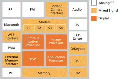
Most SoCs currently being developed have analog or mixed signal blocks, such as SerDes cores, UARTs, DACS, ADCs, PLLs, and other transceivers. Since analog does not scale as well as digital, these blocks might represent a substantial portion of the SoC. Moreover, many so-called analog blocks actually have digital-control logic. As such, an increasing amount of analog IP is really mixed signal, and with rapidly increasing SoC capacity, a single IP block might represent an extremely complex mixed signal function.
The hypothetical SoC in the figure below shows analog blocks in white and digital blocks in orange. Light orange represents mixed signal blocks with both analog and digital circuitry. In earlier process generations, some of these mixed signal blocks might have been the entire chips.
Currently, a sizable part of mixed signal chip implementation planning is done manually, which is a slow and laborious process that can lead to design errors and numerous iterations. During final assembly, the completed blocks are also placed and routed using a semi-manual process, without the aid of design rule-correct automation.
Big analog designs with digital blocks start with a schematic design in Virtuoso and then iterate over the floorplanning steps by manually placing the blocks as per the design architecture, and assigning pins for the blocks which could be analog as well as digital. Additionally, in the beginning of the design cycle, you just have the top-chip floorplan and do not have much insight into the design-implementation details.
2.1.1 Design Methodologies Supported by the Cadence Mixed Signal Solution
Schematic-driven mixed signal and netlist-driven mixed signal are two of the design methodologies supported by the Cadence mixed signal solution. Schematic-driven mixed signal and netlist-driven mixed signal are block-based methodologies sufficient for many designs when functionality can be contained in blocks with few analog-digital interfaces not critical for design performance. Schematic-driven mixed signal is a methodology used to implement mixed signal designs that have a large analog content and a small digital content (also known as big A little D - A/d). On the other hand, netlist-driven mixed signal is a methodology used to implement designs that have a large digital content and a smaller analog content (also known as big D little A - D/a).
For the Schematic-driven mixed signal flow, the top level of a design is typically represented as schematics, while the Netlist-driven mixed signal's top level is typically represented as a Verilog netlist. That is the reason why some designers refer Schematic-driven mixed signal methodology as a the schematic-on-top methodology, and netlist-driven mixed signal as the netlist-on-top methodology.
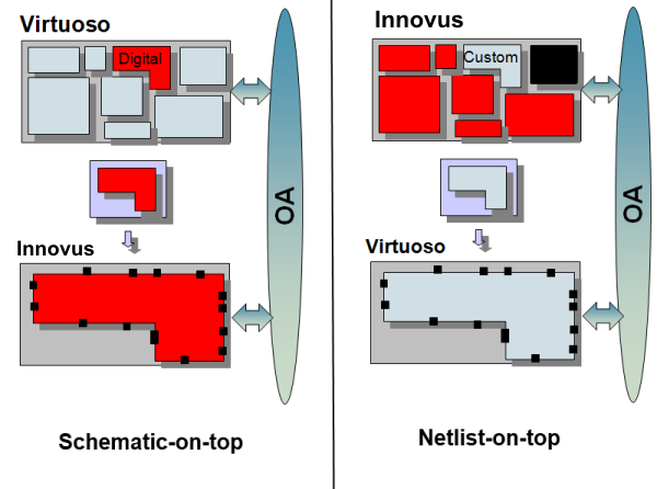
In the Cadence environment, if schematics are used for representing the top level, the design cockpit of choice is generally the Virtuoso environment, However, if a Verilog netlist is used for the top-level design, the Innovus™ Implementation System software is generally used as the design cockpit.
Traditionally, both the schematic-driven mixed signal and netlist-driven mixed signal flows have partitioned out the part of a design that is targeted for implementation in a different cockpit. For example, in the case of a schematic-driven mixed signal flow, the top level of the design is predominantly analog and is represented as a schematic containing one or more smaller digital blocks. In this case, the digital content is taken to Innovus, and once implemented and verified, brought back and re-mastered in the top-level design in Virtuoso.
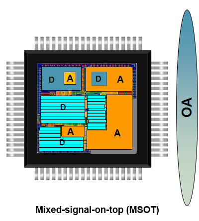
The recent trend towards the implementation of high performance mixed signal designs has created a requirement for supporting flows/methodologies that allow mixing of digital and analog content throughout the design hierarchy. The underlining OpenAccess infrastructure in the Cadence mixed signal solution makes it possible to support this design methodology through a flow that takes advantage of the functionality existing in either Innovus or Virtuoso cockpit, no matter whether the top-level design is represented as a schematic or a netlist. This methodology is referred to as concurrent mixed signal.
Cadence is addressing this challenge by introducing a new flow which draws on the strengths of the schematic-driven and netlist-driven mixed signal flows, and the interoperable Open Access database. This will allow users to easily migrate their entire design from one platform to another and take advantage of the unique features of each environment. For instance, in the new floorplanning flow, both analog and digital blocks can be floorplanned, much earlier in the design cycle when the details of these blocks are not available. These blocks are defined as blackboxes for the purpose of starting the design. The design is taken from one platform to another to enable all analysis steps, possible in the two platforms, thereby enabling users to make adjustment and more intelligent trade-offs. For example, after the top-level schematic is ready, you can run OpenAccess-based applications to generate Verilog for the top level, stitch the Verilog of the available modules, import in Innovus for blackbox-based high capacity, congestion, and timing-driven floorplanning. This helps them arrive at a higher quality block placement, pin locations, routing interface nets, and thereby lowering routing congestion. This new flow reduces the number of iterations between analog and digital designs, particularly during floorplanning, chip integration and early-and-late small/big ECOs.