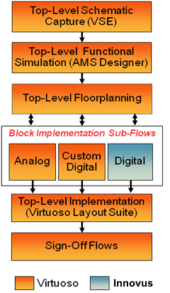
- Schematic-Driven Mixed Signal Flow
- Overview
- Top-Level Early Floorplanning
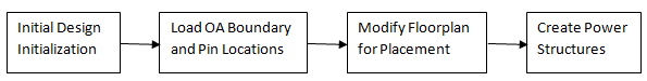
- The Analog Block Implementation Sub-Flow
- Custom Digital Implementation Flow
- Digital Block Implementation Flow
- OpenAccess Based Interoperable Flow between Innovus and Virtuoso
- Top-Level Block/Chip Assembly flow
- Virtuoso Top-Level Assembly
- Virtuoso Chip-Level Layout Assembly
- Flow Example: Power PushDown Flow for Digital Blocks in AoT Designs
5.1 Schematic-Driven Mixed Signal Flow
5.1.1 Overview
In this chapter, we will begin by discussing a high level overview of the schematic-on-top flow. In addition to covering the core flow, we will include some of the peripheral tasks both at the beginning and at the end of the flow in order to provide some needed perspective.
The terms top-down versus bottom-up design methodologies refer to the order in which a hierarchical design is implemented. Ideally, the design should be done top-down, but in reality it is more common to construct the design simultaneously using a combination of top-down and bottom-up methodology.
Ideally, the schematic capture will begin in a top-down fashion with a top-level schematic. It is this top level connectivity source that makes it possible to do early floorplanning within the Virtuoso layout environment, and differentiates this schematic-on-top implementation from the netlist-driven or netlist-driven mixed signal approach. Schematic-on-top does not mean that the schematic must exist for all the blocks in the design throughout the entire hierarchy. It only refers to the top-level. In addition, the schematics will be used to drive the implementation of any analog portions of the design. However, netlists will and should be used for most of the digital-design content.
5.1.1.1 Top-Level Schematic Capture
At the initial stages of the design, only functional and performance specifications are available. The designer has the task of deciding the optimal-design partitioning with the major sub-systems identified as sub-blocks. Normally, the design partitioning is determined by the major functional blocks, performance, and design disciplines required for the overall implementation. As a result, the design is decomposed into analog and digital functional blocks.
5.1.1.2 Functional Verification
It is important to note that both the verification and implementation flows are driven from the same schematic database, thereby ensuring consistency between the two sub flows.
5.1.1.3 Floorplanning
In the schematic-driven mixed signal flow, most of the floorplanning, in particular the top-level floorplanning is done in the Virtuoso environment, using the top down floorplanning methodology. In this flow, some or all of the sub-blocks will be created as soft blocks, as they have not been fully implemented yet.
5.1.1.4 Block Implementation Sub Flows
When it comes to physically implementing the blocks, different sub flows will be used depending on the type of block being implemented. Designs are typically partitioned into analog and digital functions. For a digital design, the block Verilog netlist, physical abstracts of standard cells and other associated files such as timing constraints are passed to Innovus. After the digital block has been implemented in Innovus, the layout view of the block is brought back into Virtuoso to replace the autoAbstract which was earlier created for the block. It is important to note that a schematic is not required for the digital blocks in the design.
5.1.1.5 Top-Level Implementation
This task involves making any final adjustments to the floorplan (in Virtuoso) now that blocks are fully implemented, routing the design and verifying all aspects of the design, which may include timing. An important note is that power connections in the design are managed using the inherited connections in Virtuoso, or using explicit power terminals across the hierarchy.
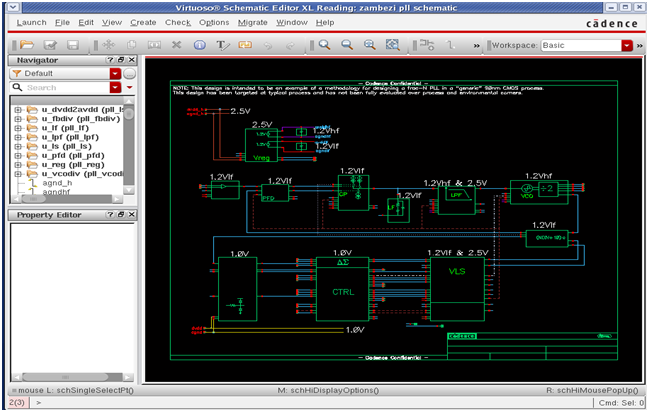
5.1.2 Top-Level Early Floorplanning
The common floorplanning tasks are:
- Configuring the physical hierarchy: This step creates what is called the physical configuration view (or
physConfig). This identifies the mapping between schematic components and layout components. It is possible for the layout views to be located in other libraries. For blocks for which user does not have a layout view, theprBoundarycan be entered using an estimate for the layout area and the pin information could be entered using the information found on the schematic symbol.
- Placing and arranging all the blocks - adjusting their location and shape. Adjust pin locations and sizes - taking advantage of the various pin alignment and optimization features available in the Virtuoso Floorplanner. You can also edit the block shape by using level-1 editing commands, which allow you to modify the block prBoundary from the top level.
- Iterative floorplan refinement - Using the automated routing tools, perform trial top-level routing to identify congestion and other routing challenges.
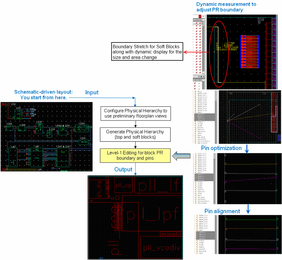
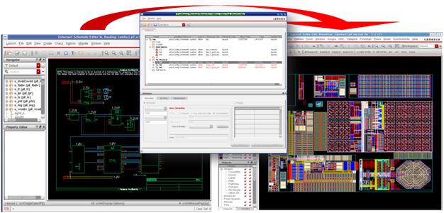
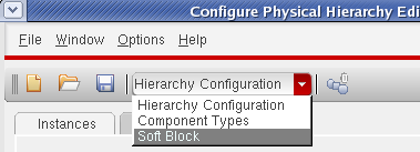
5.1.2.1 Configure Physical Hierarchy (CPH)
The CPH is used to create mapping between the schematic and the layout instances. You can create softBlocks for cells that do not have an existing layout or schematic. You can drive the pin and cell boundary snapping to grids by setting the Block Type as DIGITAL or CUSTOM.
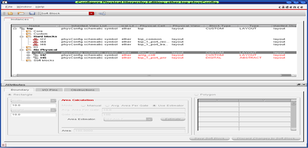
The above figures show how CPH works after launching Virtuoso Layout Editor-XL for a top-level schematic for the first time. CPH gives you control over the automated schematic-to-layout generation process without requiring the layout designer to modify the schematic.
5.1.2.2 Generate Physical Hierarchy (GPH)
This step in the flow is used to perform bottom-up hierarchical generation of layout in order to have an accurate estimation of area. The following figure illustrates the use of CPH to drive the generation of layout using GPH. GPH generates the layout for the soft blocks and instantiates the hard blocks in the design based on the bindings specified in CPH UI. This enables more accurate estimation of the area at the top level. You can access GPH using the Floorplan menu in Virtuoso Layout Editor -GXL.
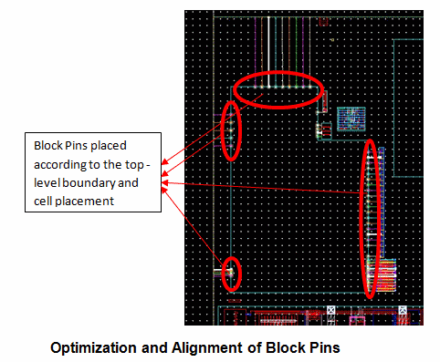
5.1.2.3 Level-1 Editing and Pin Optimization
The floorplan for the top level can be adjusted to meet the aspect ratio and the utilization factor using a host of commands from the Virtuoso Floorplanner suite.
The user can adjust and even create rectilinear boundaries for the unimplemented soft blocks by editing the prBoundary for the blocks from the top level to obtain a better packing for the floorplan. The boundaries can be stretched and chopped to achieve the desired area.
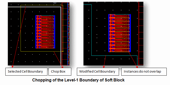
You can use the pin optimizer and the pin alignment commands to increase the routability of the design by adjusting the pin locations for these soft blocks and the top-level design. This helps in minimizing the net length.
5.1.3 The Analog Block Implementation Sub-Flow
The analog block implementation flow is the traditional flow that most Virtuoso designers use. This section provides an overview of the steps involved in this sub-flow. For more detailed description of each flow step, refer to the Virtuoso® Analog Placer User Guide.
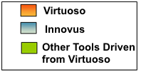
5.1.3.1 Initial Top-Level Floorplan
The assumption in this step of the flow is that the block being floorplanned is the top-level design for this sub-flow. The information derived from the top-level floorplanning (initial area estimate, width, height and the I/O pin locations) step is used in this step of the design. Although this data is just an estimate, it serves as a good start point for the flow. The real data is only known after circuit design is completed.
5.1.3.2 Schematic Capture
At this step in the flow, the circuit design is done based on the block-level specification. This is the task of capturing the schematic and making sure it is optimized to meet the specification. During this process, you can add some electrical constraints that would later get used for circuit optimization, such as matching parameter constraints, and so on. Before the design is handed off to the layout design team, layout constraints, such as placement and routing constraints, can also be added to the design.
5.1.3.3 Analog Floorplan (Also Referred to as the Cell Plan)
In this step, the initial floorplan is used to begin the layout implementation flow. Generate From Source (GFS) is run and the prBoundary and pin locations are loaded from the floorplan. After running GFS, the number and the size of the components to be placed are known, and floorplan refinement can also be done.
5.1.3.4 Analog Placement
This is the process of placing components in a design so they respect previously specified constraints. If the constraint-aware editing mode is enabled (default) during component placement, whether the devices are placed interactively or semi-manually, the placement constraints such as modgens, symmetry, alignments and orientation are enforced. For instance, if you place one component from a symmetrical pair, the other will be placed at the same time and the same distance from the shared axis of symmetry.
The Virtuoso Analog Placer (VAP - part of VLS-GXL) can be used to fully automate the component placement using the constraints previously specified by the user. For best results using VAP, there needs to be a sufficient number of constraints in a design.
5.1.3.5 Device-Level Routing
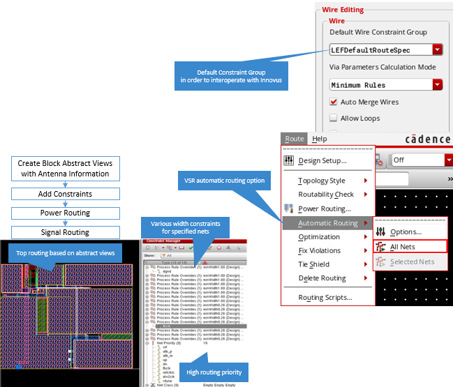
The Virtuoso Space-Based Router (VSR - part of VLS-GXL) can be used for automatic routing of the design. Alternatively, the Wire Editor (available in VLS-XL) which uses the same routing technology as VSR can be used to perform constraint-aware interactive routing.
5.1.3.6 Block-Level Sign-Off
Block-level sign-off is an entire sub flow within itself and consists of the steps necessary to make sure the design is logically correct, can be manufactured, and still meets its performance requirements. This flow is fairly standard and highly dependent both on the design-specific challenges and the foundry requirements. Refer to the Virtuoso documentation for more details on this sub-flow.
5.1.3.7 Abstract Generation
Abstract generation is required for the design assembly part of the flow, which can be considered as the layout finishing step of the flow. The Virtuoso integration of the abstract generator could be used to accomplish it. For more information, refer to the Virtuoso®Abstract Generator User Guide.
5.1.3.8 Constraint Verification
Finally, constraint compliance can be verified using the constraint checking features of the Virtuoso Constraints Manager.
The combination of the automated/assisted and constraint-driven layout features forms what is often referred to as the Rapid Analog Prototyping (RAP) flow. This flow makes it possible to quickly transform a schematic into a layout for the purpose of providing more accurate information for the floorplanning step of the flow and layout parasitics for design optimization/refinement.
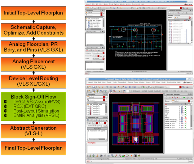
5.1.4 Custom Digital Implementation Flow
This flow is very similar to the analog block implementation flow described previously. This flow assumes that the design contains some small, non-timing constrained digital blocks (typically a few hundreds of standard cells) that need to be added to the design. Although the overall function of a particular block may be analog, there is often a need to provide some type of digital interface for control related functions, such as the calibration function, so on.
Either a schematic or netlist-driven flow could be used for the implementation of the custom digital function. For the schematic driven approach, user can create a schematic manually. However, if a gate-level netlist is available, the netlist can be synthesized using the digital block implementation flow.
The tasks and tools of this flow are the same as the analog flow except that a different placer, the Virtuoso Custom Placer (VCP - part of VLS-GXL), is used to automate the placement of the digital cells. Automatic VSR routing is done after the completion of placement. This highly automated flow, is similar to the standard digital flow. One of the main differences between this flow and the standard digital implementation flow in Innovus is the lack of a timing-driven implementation approach. This flow demonstrate that it is possible to implement a non-timing constrained digital block in a few minutes without leaving Virtuoso.
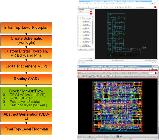
5.1.5 Digital Block Implementation Flow
This part of the flow takes advantage of the enhanced interoperability between the Virtuoso and Innovus platforms, and is made possible through the use of the OpenAccess database. Most of these tasks are typically executed by the digital designer. However, the goal is to ensure that the analog (Virtuoso) and digital (Innovus) designers are working from the same database at all times in order to maximize collaboration and reduce the chances of miscommunication. This flow has other advantages such as cross-platform ECOs, design-constraint interoperability, and a host of other advantages for the design teams.
5.1.5.1 Logic Synthesis and Design Initialization
The digital designer will synthesize the gate-level netlist and load the final verilog netlist into the Innovus platform along with the reference OA libraries for the cells. The design will be initialized with a default boundary and core rows.
5.1.5.2 Digital Prototyping and Power Planning
While traditionally not considered part of the implementation flow, this portion of the flow allows you to perform incremental floorplanning for the digital portion of the design.
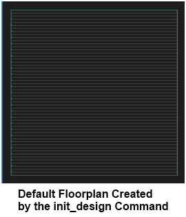
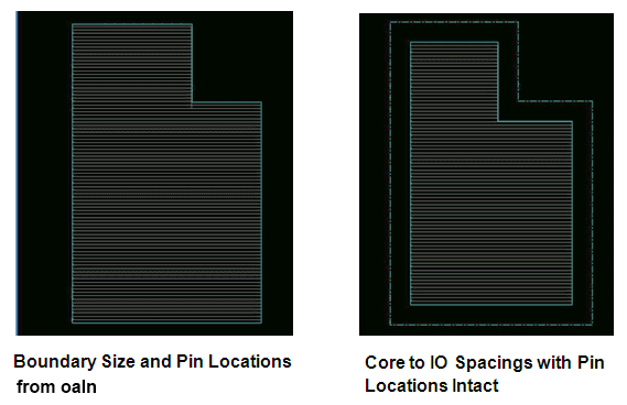
You have a choice to entirely implement the design in Innovus, or import the floorplan for the block (prBoundary and pin assignment) from the work that was earlier done in Virtuoso. Once the floorplan is imported from Virtuoso, it can be further modified in Innovus. For instance, the creation of power structures may require alteration of IO to core spacing. You can also alter the default row style created by the init_design command.
It is strongly recommended that you create the rows in Innovus if you are going to use the standard cell placer in Innovus for placing the cells in the design.
The following flow diagram shows the steps to prepare the OA cell for place and route in Innovus.
Controlling Floorplanning Information Read In from the OpenAccess Cellview
When reading in floorplanning information from the OpenAccess cellview to Innovus, you need not read in the entire cellview. You can use any of the following mechanisms to control the floorplanning information read in from the cellview:
oaIncommand in Innovus (without-filter): Use theoaIncommand without-filterif you want to read updated placement and routing information with no changes to the netlist. For example, you can use this method if you want to send a placed database to another tool to perform routing and then read back the result. Error checking is performed to make sure that the you are reading from the correct database.oaIncommand with the-filteroption: UseoaIn -filterif you want to read floorplanning information from a cellview whose connectivity does not match the current Innovus in-memory connectivity. The-filteroption allows you to load some data selectively, while not loading others. When-filteris used, error checking for database consistency (nets, instances, terminals, etc.) is disabled. While similar to Virtuoso Load Physical View (LPV), the-filteroption is only a subset and not intended to be a complete replacement.
From the Innovus 15.1 release,oaIn -filterhas been extended to support additional floorplanning objects. The-filteroption now accepts the following values:block_insts- Indicates that any CLASS PAD instances should be updated. Physical-only block instances may be added to the database if the placement status isfixedorcover.blockages- Indicates that blockages should be processed. If a blockage is attached to an instance that does not exist in the in-memory database, then it is ignored.boundary- Indicates that the design boundary information, including rows and tracks, should be updated.fixed_core_insts- Indicates that any CLASS CORE instances that have placement statusfixedorcovershould be updated. Physical-only core instances may be added to the database if the placement status isfixedorcover.floorplan- Is equivalent to specifying "block_insts blockages boundary fixed_core_insts pad_insts pin_shapes regions special_routing"pad_insts- Indicates that any CLASS PAD instances should be updated. Physical-only pad instances may be added to the database if the placement status isfixedorcover.pin_shapes- Indicates that pin shapes should be read.regions- Indicates regions should be updated.regular_routing- Indicates that nets should be processed and regular routing (and associated shield net wiring) and net constraints updated.special_routing- Indicates that nets should be processed and special routing (except shield nets wiring) should be read.
When
-filteris not specified, all information is read from the OpenAccess cellview. When-filteris specified, only the object types that are chosen is read from the OpenAccess cellview. Additionally, when reading pin_shapes or instances, information in the cellview that refers to terminals or instances that do not exist in memory is ignored.
ecoOaDesign: UseecoOaDesignif you want to read a new netlist and as much of the original cellview's information as possible. This method applies to a timing eco or post-mask eco flow. In these cases, the amount of change to the netlist is typically small and the goal is to disturb as little of the original information as possible for timing closure or "frozen-metal" eco purposes.
Incremental Floorplanning
As the prBoundary brought over from Virtuoso includes the IO to core spacing, you will need to update the IO to core spacing so that structures such as core rings can be created. This is shown in later steps in this document.
Note: Do not use the Specify Floorplan command because it is not an incremental command and will reset the boundary shape to rectangular in case the prBoundary is rectilinear. It will also reinitialize the pin and pad placements. Instead, use the following command to update the IO to core spacing:
changeFloorplan [-noSnapToGrid] [[-coreToLeft value][-coreToBottom value][-coreToRight value][-coreToTop value] | [-coreToEdge {left bottom right top}]]
This will preserve the pin and pad placements done on the rectilinear edges of the boundary while keeping the prBoundary structure intact.
To change the row style and size, you can use the commands cutRow and createRow.
The cutRow command allows you to delete the site rows that intersect with the specified area.
cutRow [-area box | -object string | -selected][-halo float | {-leftGap float | -rightGap float | -topGap float | -bottomGap float}][-site siteName] [-keepCell]
The createRow command then allows you to specify the core rows as per your requirement.
createRow -site siteName [-area {x1 y1 x2 y2}] [-spacing distance][-noAbut | -noAbut1st][-flip1st][-noFlip]
cutRow to remove unwanted rows
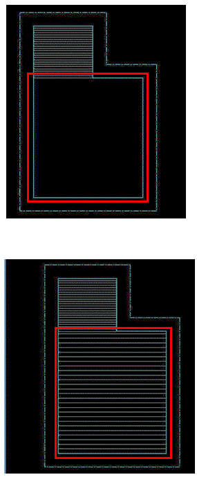
New rows created by createRow
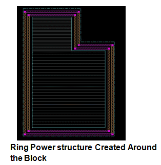
Power Routing
After the floorplan for the block has been fixed, the power routing for the block can be performed. The space between the IO and the core region created can be used to create a power ring structure or you might choose to create stripes or custom power topology as per the design specifications.
5.1.5.3 Digital Foundation Flow for Block Implementation
The digital foundation flows are a collection of scripted flows are delivered as a part of Innovus. There are different flows to address different types of design challenges such as hierarchical design, low power and so on. There is also a basic full flat implementation flow.
This Innovus based flow consists of all of the tasks listed below:
Clock tree synthesis, timing-driven logic optimization, timing-driven placement and routing, signal integrity analysis and fixing (crosstalk), sign-off extraction and timing analysis, logic equivalency checks using Conformal, and saving the design into OpenAccess. Timing analysis refers to the process of running Static Timing Analysis (STA) to validate the overall timing of the design, based on the timing constraints created for the digital blocks. For instance, STA checks that signals are available at the input to flops for a pre-defined amount of time before the clock arrives (setup check) or that signals are available long enough at the input to be properly captured (hold check).
The OpenAccess design saved in Innovus can then be opened in Virtuoso.
5.1.5.4 Layout Remaster
The remastering for the digital instance at the top level involves replacing the unimplemented digital block view with the fully implemented view saved in Innovus. However, when the implemented block layout is opened in Virtuoso, you will see only the abstract views instead of seeing the layout masters for each of the standard cell instance. Therefore, you must perform another step in the flow to replace the abstract references with their corresponding layout references (remastering) before the design can be verified in Virtuoso. A menu pick is provided in Virtuoso to make this step quick and simple. It can be accessed in the layout window under Tools -> Remaster Instances.
5.1.5.5 Sign-Off Flow
This step in the flow is simpler than for the other sub-block flows because the post-layout electrical verification has already been done in Innovus.
5.1.5.6 Top-Level Floorplan
We now have the final top-level floorplan with the digital block fully implemented.
5.1.6 OpenAccess Based Interoperable Flow between Innovus and Virtuoso
The figure below illustrates the interaction between Virtuoso and Innovus for fully implementing the contents of digital block in a design.
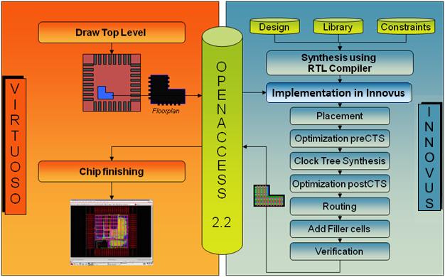
As can be seen from the illustration above, the chip finishing and the final assembly of the design will be done in the Virtuoso cockpit. This step in the flow is another differentiating factor between the schematic-driven mixed signal and netlist-driven mixed signal flows.
5.1.7 Top-Level Block/Chip Assembly flow
The top-level mixed signal block/chip assembly flow is a continuation of the bottom-up implementation flow. Planning for the top-level assembly typically starts at the beginning of the overall flow, before any of the sub-blocks have been implemented. You might have already performed some trial top-level routing in order to determine routing feasibility and any performance impact to critical signals.
At this stage of the flow, we assume that all of the sub-blocks are in their final form as implemented by their various sub-flows described previously in this document. In other words, the OpenAccess database contains the complete layout and abstracts, any constraints relevant to the top-level assembly, and so on.
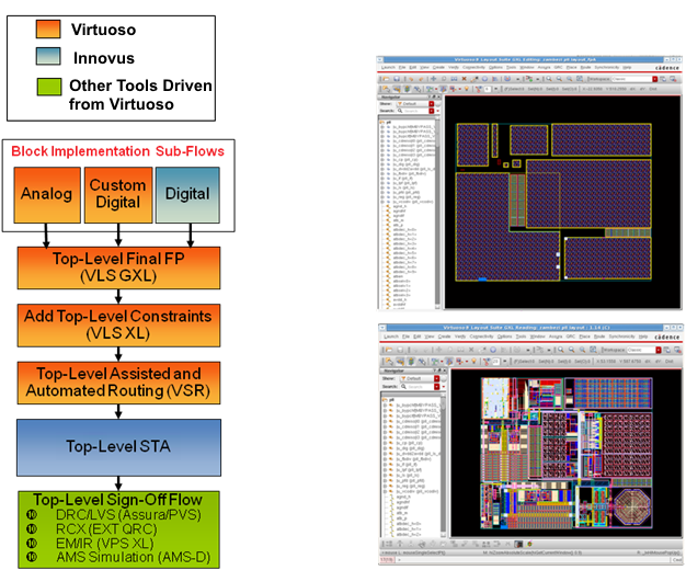
5.1.7.1 Top-Level Final Floorplanning
At this stage, any final adjustments can be made to the top-level floorplan to account for any changes to final block sizes and IOs. This will result in the final design placement.
5.1.7.2 Add Top-Level Constraints
The top-level layout may contain additional constraints. These are typically various routing type constraints. These constraints may be driven from the schematic, added directly to the top-level layout, or automatically or manually propagated upward from lower level blocks using the new hierarchical constraint management features available from the Virtuoso IC 6.1.5 release.
5.1.7.3 VSR Routing
The Virtuoso Space-Based Router (VSR) supports a wide variety of routing constraints and is typically used in a more automated flow when routing the top-level design. However, the interactive constraint-aware wire-editing features in Virtuoso can be used for selective nets.
5.1.7.4 Top-Level STA Task (Optional)
Performing top-level STA requires the existence of a Verilog netlist at the top level which represents the interconnection between the various blocks at the top level. If a Verilog netlist is available, or one can be created by the design team, it is possible to perform STA at the top level assuming that certain blocks have their timing characterized in the .lib format used by the STA tool.
5.1.7.5 Top-Level Sign-off
This is a complex and multistep flow that varies depending on the design-specific challenges, target foundry requirements, and so on. It involves a combination of physical verification tasks (DRC, LVS) and electrical verification tasks (MSPS, EM/IR, functional verification). A typical list of tasks are given below. All of these tasks can be driven directly from the Virtuoso environment. The AMS-D simulator is typically used here just as it was used earlier in the design flow. However, the simulations will now be based on extracted layout netlists with parasitics. This simulation can make use of the advanced features of ADE, such Virtuoso Parasitics Aware design (VPAD) to rapidly switch between pre-layout schematic and post-layout extracted representations of the design and debug parasitic-related problems.
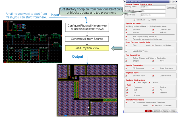
5.1.8 Virtuoso Top-Level Assembly
This figure below illustrates how connectivity and constraint information captured in the schematics representing the top-level of the design is used to create an initial layout using the placement information provided by the floorplan view. At this step, the floorplan is loaded using the Load Physical View (LPV - part of VLS -XL) utility in the Virtuoso layout environment, which will place all of the sub-blocks according to the floorplan. Note that as an intermediate step, you should have configured the physical hierarchy (CPH) to use the abstract masters.
5.1.9 Virtuoso Chip-Level Layout Assembly
The figure below shows a more detailed description of the VSR-based top-level block assembly flow. The routing on the top-level layout is being performed by the VSR engine, using abstracts for each of the sub-blocks, and using the supplied constraints. You can choose to perform VSR routing interactively or by using a more automated approach.
5.2 Flow Example: Power PushDown Flow for Digital Blocks in AoT Designs
In the schematic-driven mixed signal flow or the Analog-on-Top (AoT) methodology, the top-level floorplanning is done in the Virtuoso environment. Digital sub-blocks are created as soft blocks because they have not been fully implemented yet. The power shapes created during top-level floorplanning in Virtuoso are pushed down into the digital blocks. The Verilog netlist, physical abstract, and other associated files, such as timing constraints, are then passed to Innovus™ Implementation System for complete physical implementation of the digital blocks. After a digital block has been fully implemented in Innovus, the layout view of the block is brought back into Virtuoso for design assembly. The fully implemented block now replaces the abstract that was earlier created for the block in Virtuoso.
This chapter covers the procedure for implementing a digital block in Innovus with power shapes created during floorplanning in Virtuoso. In the example used in this chapter, the block pll_dig is implemented as a digital block. The example illustrates the typical steps for running this flow. You can modify the floorplanning and implementation steps according to your needs.
To implement a digital block in Innovus using the power shapes created during top-level floorplanning in Virtuoso, you need to perform the following basic steps:
- Perform top-level floorplanning in Virtuoso.
- Push power shapes into the digital block.
- Implement the digital block in Innovus.
- Bring back the digital block into Virtuoso for design assembly.
Note - The snapshots used in this example are from IC 6.1.6 ISR3 and Innovus 15.10.
5.2.1 Performing Top-Level Floorplanning in Virtuoso
To perform top-level floorplanning in Virtuoso, perform the following steps:
- Open the top-level schematic of the design in Virtuoso.
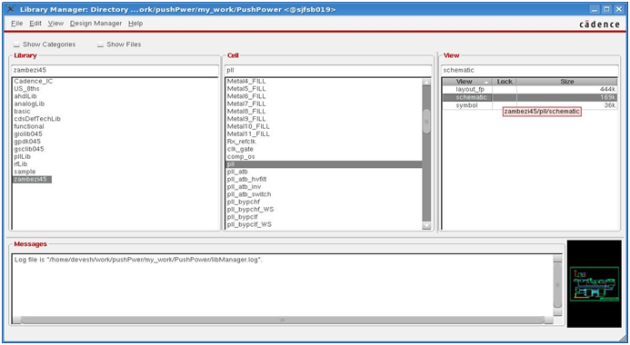
- In CIW, select Tools - Library Manager.
- In the Library Manager form, select the required library, cell, and view (
schematic) to open the top-level schematic.
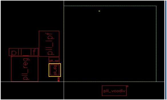
The top-level schematic contains a symbol for the block that needs to be implemented as digital block . The block does not have any power or ground pins as shown below. It needs to be supplied power by the top-level digital power and ground nets. The sample top-level schematic below contains a symbol for thepll_digblock.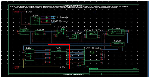
- In CIW, select Tools - Library Manager.
- View the block-level Common Power Format (CPF) file to get the power and ground names for the digital block.
- Open the block-level CPF file in any editor.
- Note the power supply net name specified in the file for the digital block. This helps you determine the block's power pin that will be connected to the top-level digital power net.
- Note the ground net name specified in the block CPF file. This specifies the ground pin that will be connected to the top-level ground net.
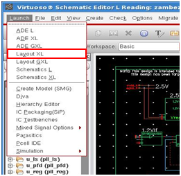
- Launch VXL to start the creation of the top-level floorplan.
- In Virtuoso Schematic Editor, select Launch - Layout XL from the menu bar.
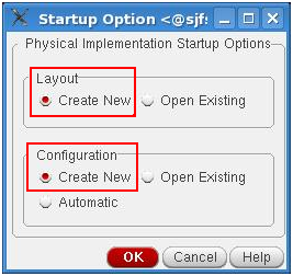
The Startup Options form is displayed. -
In the Startup Options form, select the options for creating new layout and configuration views and click OK.
- In the New File form that is displayed, specify a new name for the layout view, such as
layout_WS, in the View text box and click OK.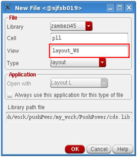
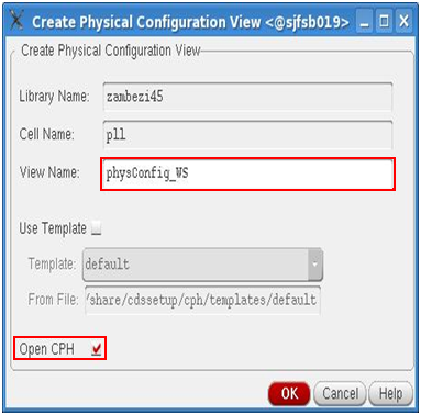
- In the Create Physical Configuration View form that is displayed next, specify a name for the configuration view in the View Name text box and select the Open CPH check box to open the Configure Physical Hierarchy form in which you will configure the top-level floorplan. Click OK when done.
- In Virtuoso Schematic Editor, select Launch - Layout XL from the menu bar.
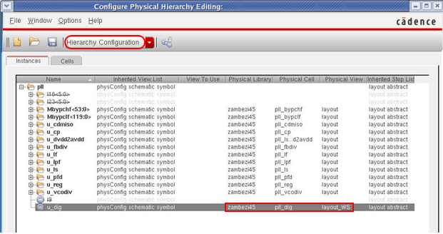
- Create a top-level floorplan using the Configure Physical Hierarchy (CPH) form. CPH is used to specify the hierarchical bindings between schematic and physical views. It also serves to specify soft block parameters to be generated by Generate Physical Hierarchy (GPH). As the new layout view you specified in the New File form does not exist yet, it will be generated later by GPH.
As you have only the pin information for the digital block from the symbol at this stage and do not have a schematic available for any hierarchy details, you can only create a blockBlackBox for the digital block. After creating the blockBlackBox for the digital block, you can add power and ground pins as per the net names specified in the CPF file for the digital block.- To create a blockBlackBox for the digital block with an estimated boundary, perform the following steps:
- In the default Hierarchy Configuration mode, enter the library, cell, and, view name for the digital block in the Physical Library, Physical Cell, and Physical View columns, respectively. The view name should be the new layout view name you specified in the New File form in the previous step.
- Switch to the Soft Block mode in the CPH form. The Soft Block mode lets you define the soft blocks that will be created by the Floorplan – Generate Physical Hierarchy command.
- In the Soft Block mode, expand the No Physical list and select the digital block. Next, right-click the block and select Edit Soft Block Parameters from the context menu.
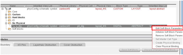
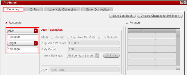
This makes the Attributes section editable for the selected block. - In the Attributes section of the CPH form, you can set up the block's boundary as per your estimate. Specify the block's width and height in the Width and Height text boxes, respectively, on the Boundary tab.
- In the default Hierarchy Configuration mode, enter the library, cell, and, view name for the digital block in the Physical Library, Physical Cell, and Physical View columns, respectively. The view name should be the new layout view name you specified in the New File form in the previous step.
- To add power and ground pins to the digital block, perform the following steps:
- On the I/O Pins tab in the Attributes section of the CPH form, add two pins with the following specifications:
- Net Name: power_net_name Term Name:
power_net_nameTerm Type:inputOutputSig Type:supply - Net Name:
ground_net_nameTerm Name:ground_net_nameTerm Type:inputOutputSig Type:ground
Here,power_net_nameandground_net_namerefer to the power and ground net names identified from the block CPF file in Step 2. In the sample screenshot below,power_net_nameisVDDandground_net_nameisVSS.
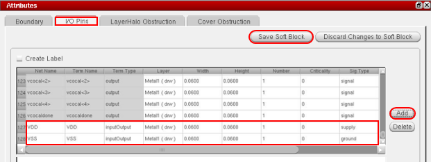
After adding the pin details, click the Save Soft Block button. - Net Name: power_net_name Term Name:
- In the No Physical list, change the Block Type from
CustomtoDigital. This changes the snap grid for the pins and boundary to the place & route grid instead of the manufacturing grid. In addition, set Type asAbstract.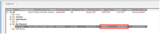
- Right-click the top-level cell and select Define Top Level Parameters from the context menu.
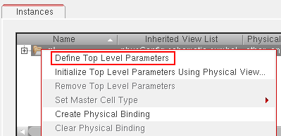
- Save the top level parameters as is with no change.
- On the I/O Pins tab in the Attributes section of the CPH form, add two pins with the following specifications:
Note: As is the case with the Innovus timing analysis flow for mixed signal designs, the top level is flattened using the
assembleDesigncommand in Innovus and then the flattened view is saved using thesaveDesigncommand. Ensure that the top-level power and ground nets are marked as global in Virtuoso. If not, it can lead to problems while saving the flattened view withsaveDesignin Innovus. Innovus will report the following error:**ERROR: (IMPOAX-1085): Cannot override the connection of instance terminal 'SN' of instance 'I0/preset_int_reg\[5\]' connected to net 'tie1' to global net 'VDD_1P2' as A physical-only instTerm cannot connect to a net located in a different occurrence. Check if the terminal is connected to a supply or tieHi/Lo net in the Verilog.The reason for this error is that the block-level power and ground pins are not in the original block symbol (verilog netlist) and are added manually, which causes them to be considered as physical-only pins. The top-level power and ground pins, however, are part of the original logical netlist (schematic) and are hence not marked as physical-only pins. Therefore, after
assembleDesignand the subsequentsaveDesign, Innovus tries to connect a physical-only instance terminal with a net that exists in the logical domain, and reports the above error. - To create a blockBlackBox for the digital block with an estimated boundary, perform the following steps:
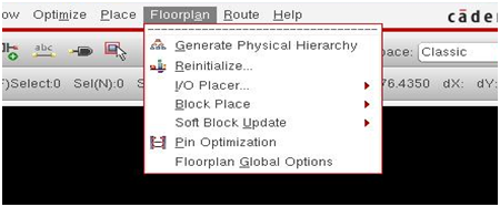
- Generate the full physical hierarchy.
- From the layout, select Floorplan - Generate Physical Hierarchy.
-
In the Generate Physical Hierarchy form, click OK.
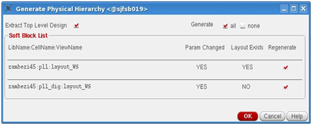
The following layout is created initially and you can see the digital block created:
- From the layout, select Floorplan - Generate Physical Hierarchy.
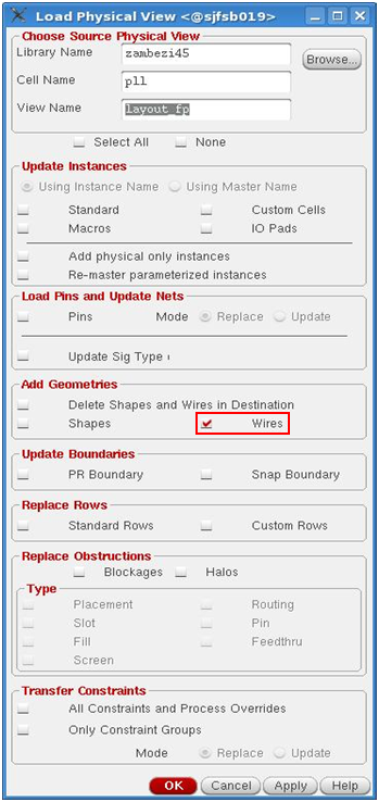
- Load the placement floorplan. To get the boundary size and the instance and pin locations for the top-level, use an existing view:
- From the layout window menu bar, choose File - Load Physical View.
- In the Load Physical View form, specify details of an existing cell view that you want to open.
- The Select All check box is selected by default. First, select the None check box to deselect all instances. Then, select the instance check boxes (Standard, Custom Cells, Macros, and IO Pads), Pins, and PR Boundary check boxes as shown below:
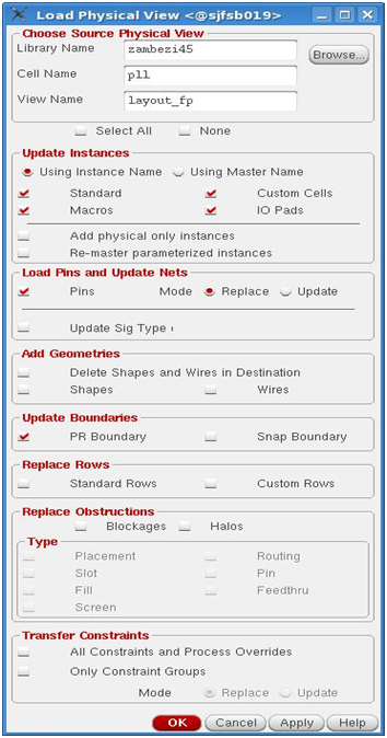
- Click OK.
- Specify top nets as power and ground:
- Invoke the Navigator window by selecting Window - Assistants - Navigator.
- Invoke Properties Editor by selecting Window - Assistants - Property Editor.
-
In the Navigator window, search for the top-level net that is to be specified as a power net and change Signal Type to
powerfor that net in Property Editor. In the example below, top netdvddis specified as a power net.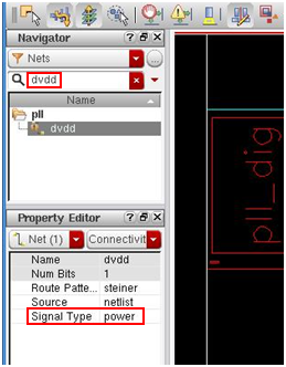
-
In the Navigator window, search for the top-level net that is to be specified as a ground net and change Signal Type to
groundfor that net in Property Editor. In the example below, top netdgndis specified as a ground net.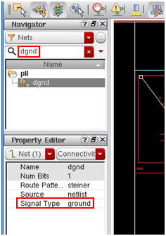
- Propagate the power and ground nets on the digital cell instTerms as per the top-level nets. The top-level net is connected with the instTerms so that the push command can identify which net to create at the lower level for the top-level power or ground nets.
- Select the digital block that you will be implementing later in Innovus.
- Select Connectivity - Nets - Propagate and scroll to the end of the Propagate Nets form.
- Assign the block power terminal to the top-level power net. In the sample screenshot below, the block terminal
VDDis assigned to top power net,dvdd. - Assign the block ground terminal to the top-level ground net. In the sample screenshot below, the block terminal
VSSis assigned to top ground net,dgnd.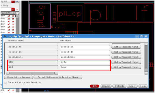
- Click OK.
- Place and optimize the pins for the digital blockBlackBox as per the top-level floorplan:
- Select the digital block.
- Select Floorplan - Pin Optimization.
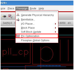
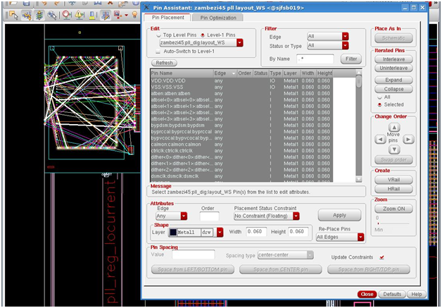
This displays the Pin Assistant form. - On the Pin Placement tab of the Pin Assistant form, and select Level -1 Pins.
- Notice that the digital block is highlighted. Select all the pins for the block in the list box on the Pin Placement tab and view the flightlines in the main window.
- Click the Pin Optimization tab.
- Click the Selected mode and specify line-via as Spacing Type.
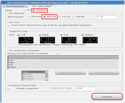
-
Click the Optimize button.
-
After pin optimization of the block, the flightlines look as follows:
5.2.2 Pushing Power Shapes into the Digital Block
Before you push power shapes into the the digital block, you need to create the power plan at the top level and ensure that the topology is set correctly on the power shapes to be pushed down. To do so:
- Create the power plan at the top level. To load the power stripes:
- Select File - Load Physical View.
- Specify the required library, cell, and view name.
- Select only the Wires option and click OK.
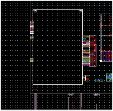
The canvas appears as follows after the power routes have been loaded: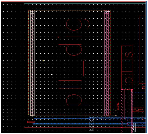
Note: Use Virtuoso Space-based Router (VSR) power planner for power planning so that the correct topology (for example, stripes in this case) is set on the power shapes to be pushed down. The Power menu is available in IC 6.1.6. For IC 6.1.5, you need to launch RIDE from the layout canvas for power planning.
You can select the power stripes on top of the digital block and set it in the CIW as follows:geGetSelSet()~> topology = “stripe”
This needs to be done only if you are not using IC 6.1.6.
- Push down power shapes:
- Select the digital block into which you want to push power shapes.
-
From the layout window menu bar, select Floorplan - Soft Block Update - Push Into Blocks.
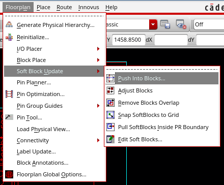
This opens the Push Into Blocks form. - The library and cell view details are filled by default in the Push Into Blocks form based on the selected block. Click OK to push the power shapes into the new
layout_pushedview that is created by default.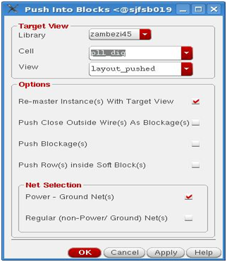
The top-level power net(dvdd)shapes are pushed as block power terminal(VDD)shapes and the top-level ground net(dgnd)shapes are pushed as block ground terminal(VSS)shapes into the digital block. If the top-level nets had not been marked as power and ground earlier, the top-level shapes would have been pushed as blockages as only the Power - Ground Net(s) check box is selected in the Push Into Blocks form.
The power shapes are pushed down in the new viewlayout_pushedand removed from the top level. The new view is replaced at the top level and is used in Innovus to implement the block.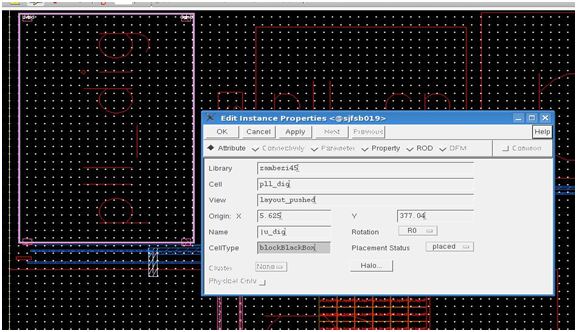
- Review the block power structures:
-
Open the newly created view by selecting File - Open and specifying the required cell view details.
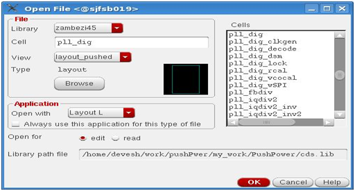
- Click OK.
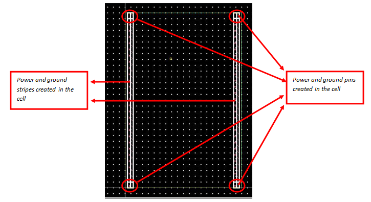
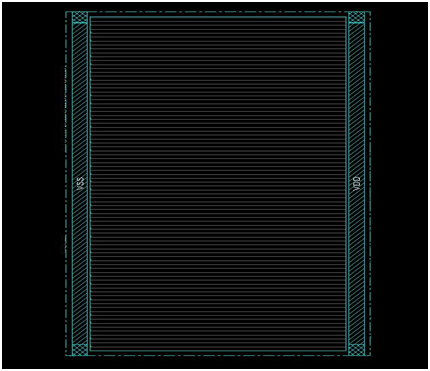
Select the power and ground stripes and check that the net name is nowVDDandVSSfor the pushed shapes. You can also view the pinsVDDandVSScreated at both the ends for the stripes that have been pushed down.
Note: If you are not using IC 6.1.6, you need to re-establish the topology for the power stripes using the following steps. Otherwise, this is automatically handled in the 6.1.6 release:- Select both the power routes and check that the topology is set to none by using the following skill command:
geGetSelSet() ~> topology
This will return "none". - Set the topology back to stripe by selecting the shapes and typing the following skill command:
geGetSelSet() ~> topology = “stripe”
Setting the correct topology is important to fully utilize the capabilities of the Special Router in Innovus.
- Select both the power routes and check that the topology is set to none by using the following skill command:
-
- Save the pushed down view as an OpenAccess cell and exit Virtuoso:
- Save all the cell views.
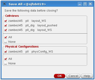
- Exit Virtuoso.
- Save all the cell views.
5.2.3 Implementing the Digital Block in Innovus
To implement the block in Innovus and save the resulting view in OpenAccess, perform the following steps:
From where is the tech information read? If an OpenAccess design is read, the tech graph is analyzed from the design_lib that contains the cellview. If a Verilog netlist is read with OpenAccess reference libraries, then the first library in the OpenAccess ref lib list is used for the tech. This means that the order of the ref libs is important when a Verilog netlist is used. Note: Additionally, sites and vias can be read from other libraries even though they are mostly considered to be tech information. Select Power - Connect Global Nets from the Innovus menu bar to open the Global Net Connections form where you can check the power and ground connections for the block. The design appears as follows after OpenAccess load. Type the following command at the Innovus shell to start placement: The design appears as follows after placement and routing.set init_verilog pll_dig.vgset init_top_cell pll_digset init_oa_ref_lib {gsclib045 gpdk045 giolib045}set init_pwr_net {VDD}set init_gnd_net {VSS}init_designwin
The design appears as follows after initialization. 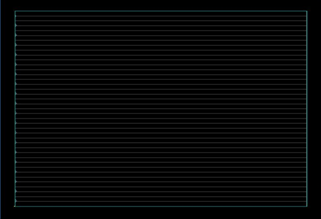
oaIn zambezi45 pll_dig layout_pushedchangeFloorplan -coreToEdge {8 2 8 2}read_power_intent -cpf pll_dig.cpfcommit_power_intent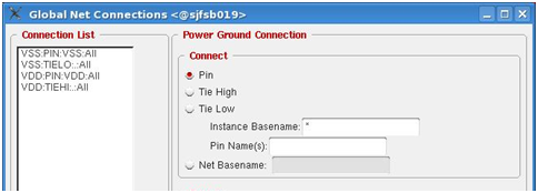
place_designdbDeleteTrialRoutesroute -connect { corePin } -nets { VDD VSS }generateViasrouteDesignverifyConnectivity -noAntennaverifyConnectivity. The -noAntenna option allows for the dangling wires at the end of the rows.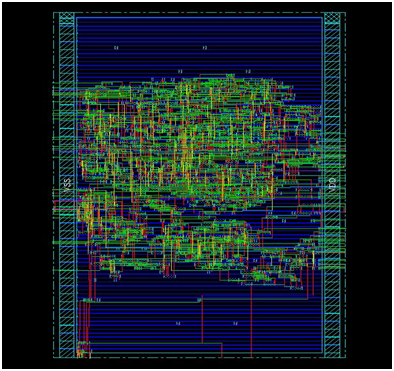
saveDesign command. Specify a new view name, such as pnr, while saving the designsaveDesign -cellview {zambezi45 pll_dig pnr}
5.2.4 Bringing Back the Digital Block into Virtuoso for Design Assembly
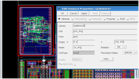
Remaster the digital block at the top level in Virtuoso to use the implemented view. To do so:
- Invoke Virtuoso and open the required cell.
- Select the digital block and invoke the property editor.
- Change the view name for the digital block from
layout_pushedto the new view name you specified while saving the design in Innovus. In the example below, the new view name ispnr.