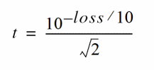
1
rfLib Library
The elements contained in the RF library, rfLib, are organized into the following categories:
-
Everything, lists all elements inrfLib - Baseband_components
- Butterworth_filters Category
- Chebyshev_filters Category
- Measurements Category
- Passband_components Category
- RF_components Category
- Testbenches Category
- WCDMA_components Category
- Wireless Components Category
The rfLib elements support the design of both RF circuits and RF systems.
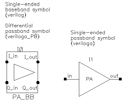
Baseband_components
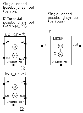
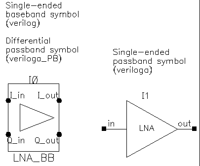
The Baseband_components category contains the top-down baseband models of common architectural function blocks. The default view of these models is the baseband view (called veriloga) but most models in this category also have a differential passband view (called veriloga_PB). The BB_loss and VGA_BB models are exceptions because they are meant only for baseband analysis and have no passband view.
The models in this category provide a fast method of mapping RF system specifications to detailed RF designs. The baseband models facilitate fast evaluation of candidate RF architectures specified with DSP metrics.
Baseband models are behavioral models that sacrifice some accuracy for increased simulation speed. Such sacrifices are usually acceptable in architectural studies because many implementation-dependent details do not affect high-xlevel decisions. The modeling approach taken in top-down design is to simulate only those effects that drive the decisions at hand.
Baseband modeling does not replace passband modeling because some effects missed by equivalent baseband models can affect high-level decisions. However, the application of baseband models early followed by passband models later minimizes the number of slow simulations needed at low levels of design abstraction. Baseband models help you to quickly weed out designs that would surely fail tests simulated with passband models.
The cells in the Baseband_components category are:
- BB_driver
- BB_loss
- BB_shifter_combiner
- BB_shifter_splitter
- BB_xfmr
- cap_BB
- dwn_cnvrt
- HilbertTr_BB
- ind_BB
- IQ_demod_BB
- IQ_mod_BB
- LNA_BB
- PA_BB
- res_BB
- rfVsourceBB
- up_cnvrt
- VGA_BB
BB_driver
The BB_driver element, also called as Baseband Driver, senses a baseband voltage signal and amplifies it.
Parameters
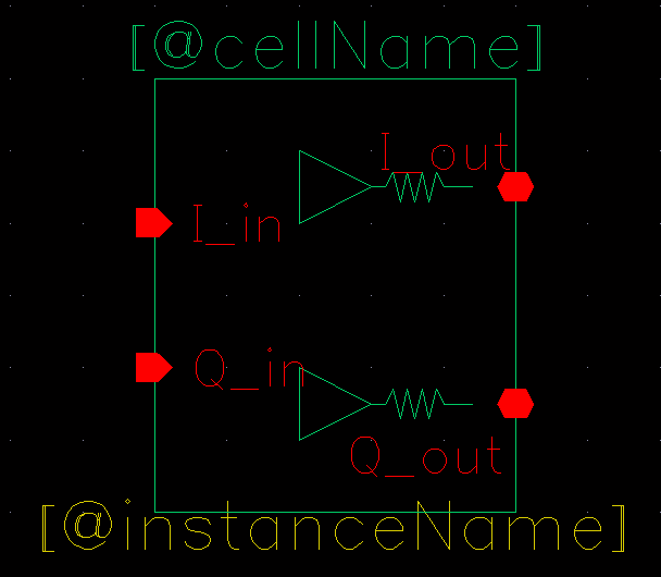
BB_loss
The BB_loss element is designed to be used with error vector magnitude (EVM) calculations. EVM is defined in terms of an ideal receiver or transmitter. If you want to remove a filter’s response from the ideal receiver model while leaving only the passband attenuation, replace the filter with a BB_loss element and give it the same insertion loss as the filter. There is no passband view or counterpart for this model.
Parameters
BB_shifter_combiner
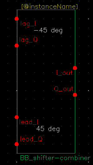
Parameters
BB_shifter_splitter
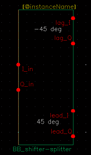
Parameters
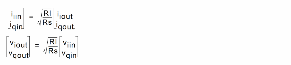
BB_xfmr
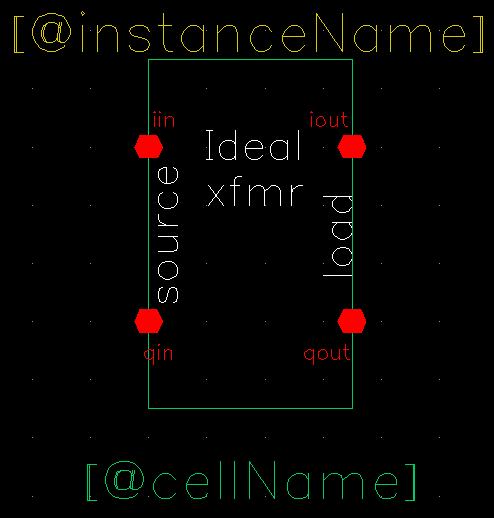
The purpose of the BB_xfmr, also known as Ideal Transformer, is to help designers transform between different resistances.
Parameters
- Inputs: i and q input voltages, i and q output currents.
-
Outputs: i and q output voltages, i and q input currents, defined as:
cap_BB
The following figures show the baseband and differential passband capacitor models.
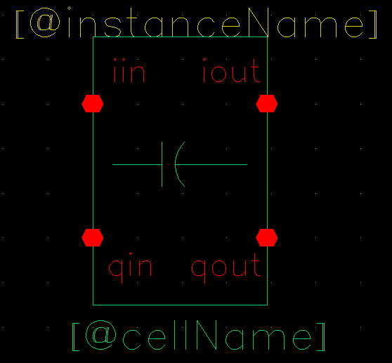
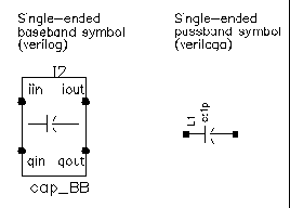
The capacitor is the mathematical dual of the inductor.
The following figure shows the capacitor model.
Parameters
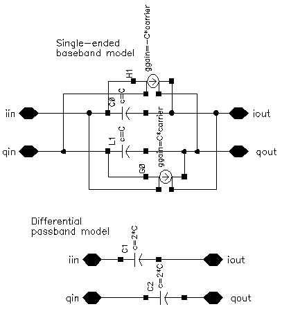
dwn_cnvrt
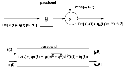
Figure 1-1 The following figure shows the Baseband and Passband Mixer Models
dwn_cnvrt model is a baseband equivalent model of a mixer used to convert from RF to IF. There are some minor differences in the baseband models that depend on whether conversion is up or down. Figure 1-2 shows what the model does.
Figure 1-2 Calculations for dwn_cnvrt Mixer
HilbertTr_BB

ind_BB
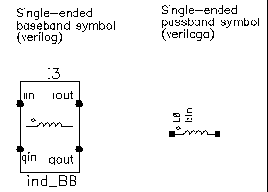
The baseband inductor model requires one additional parameter besides the inductance, the carrier frequency. Figure 1-4 shows equivalent schematics of the baseband and differential passband inductor models. The inductor models are noiseless.
IQ_demod_BB
Figure 1-5 Baseband and Passband IQ Demodulator Models
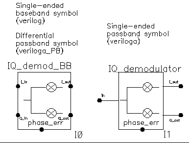
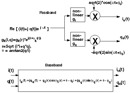
The IQ_demod_BB converts RF (or IF) to baseband. Figure 1-6 shows exactly what the passband demodulator model does. The parameters are like those in the modulator blocks except saturation is specified by input referred IP3 instead of by 1 dB compression point. IP3 was chosen over the 1 dB compression point for specifying saturation because the demodulator usually lies in the receive path and receiver blocks are usually specified with IP3.
Figure 1-6 IQ Demodulator Calculations
IQ_mod_BB
Figure 1-7 Baseband and Passband IQ Modulator Models
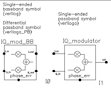
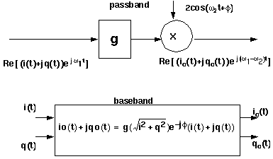
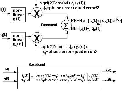
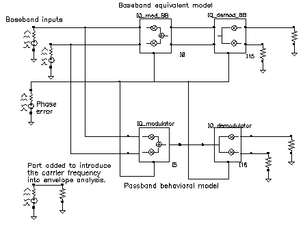
The IQ_mod_BB converts baseband signals to RF or IF. Figure 1-8 summarizes exactly what the passband IQ modulator model does. The only difference between the baseband and passband models is carrier suppression. The non-linear functions, gi and gq, are specified by their available power gain and 1dB compression points just as in the power amplifier. The functions γi and γq characterize AM/PM effects in each mixer and are specified by the same parameters that specify power amplifier AM/PM conversion. Because noise is always added at the input, and the input is at baseband in this case, the noise sources are not doubled as they are in the power amplifier or LNA models. Noise figure is defined with reference to one input. Noise is injected at both inputs but the noise injected at just one input alone produces the specified noise figure. Thus, the noise figure parameter should be interpreted as noise figure per input. This model also includes a parameter called quadrature error which specifies how far away the two local oscillators signals are from being exactly in quadrature.
Phase error is the voltage on the phase error pin. The phase error pin has a fixed noiseless resistive input impedance of 50 ohms. The phase error pin can be used to introduce a dynamic phase error or phase noise. Phase noise can be fed into the phase error pin from a phase-domain PLL model or from a Port. Noise in Port models can be specified either by the internal resistance or by a data file that tabulates a power spectral density. The phase error pin can also be driven by a ramp or circular integrator output to model a frequency error between the incoming carrier and local oscillator.
The following parameters specify the IQ modulator. The available power gain and one dB compression point are explained first. The effects of the phase_error pin and the quadrature error parameter are discussed at the end of this section.
Figure 1-8 IQ Modulator Calculations
LNA_BB
Figure 1-9 Baseband and Passband Power Amplifier Models
MPSK
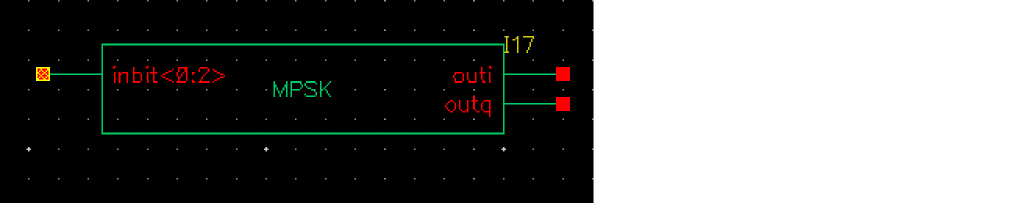
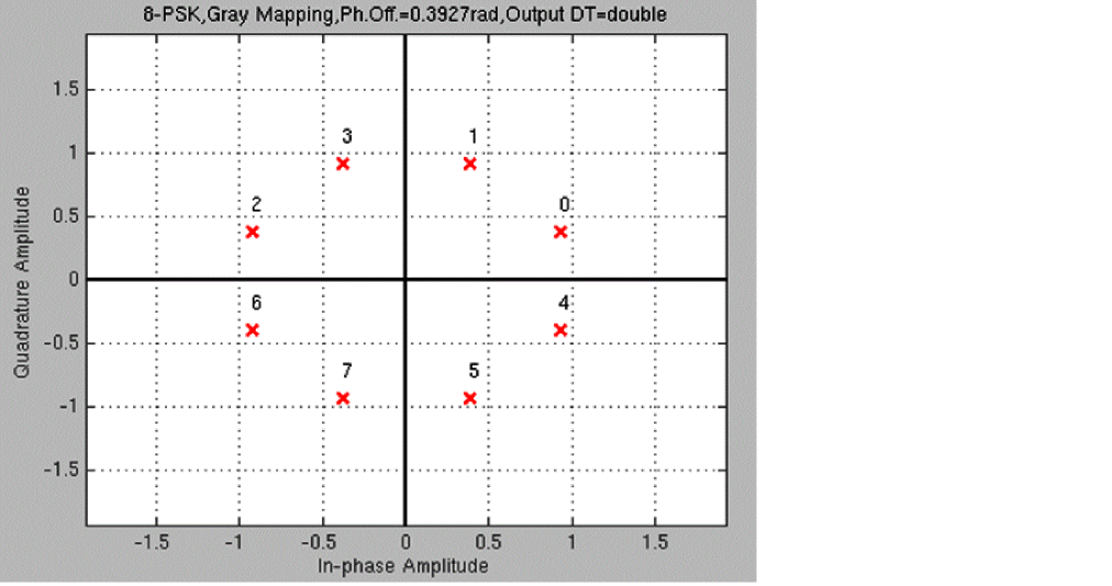
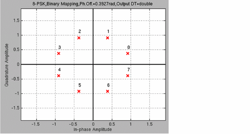
MPSK takes in a bit signal or generates a pseudo-random bit stream internally and then generates an unfiltered I and Q modulating signal at the output. The number of PSK states is eight, and the output is generated as points on a unit circle.
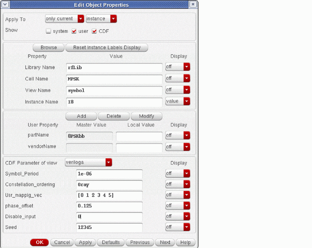
veriloga as the CDF Parameter of view.Figure 1-10 Constellation Map For MPSK
PA_BB
Figure 1-11 Baseband and Passband Power Amplifier Models
The following parameters specify the power amplifier model.
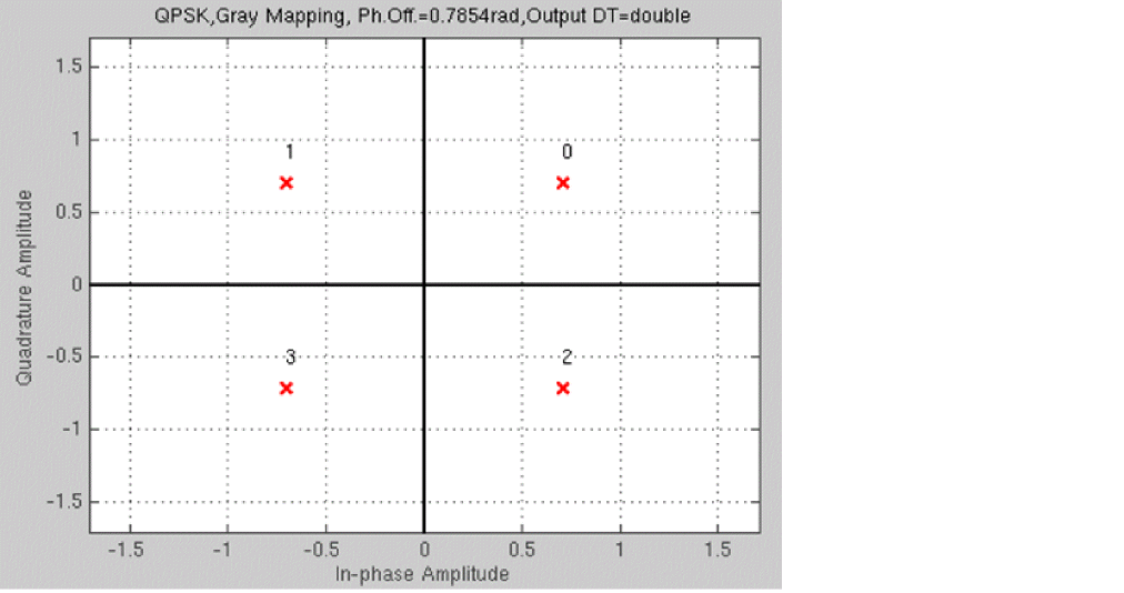
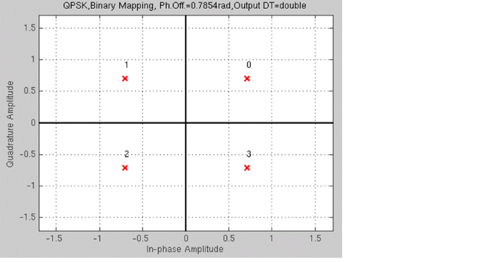
QPSK

QPSK takes in a bit signal or generates a pseudo-random bit stream internally and then generates an unfiltered I and Q modulating signal at the output. The number of PSK states is four and the output is generated as points on a unit circle.
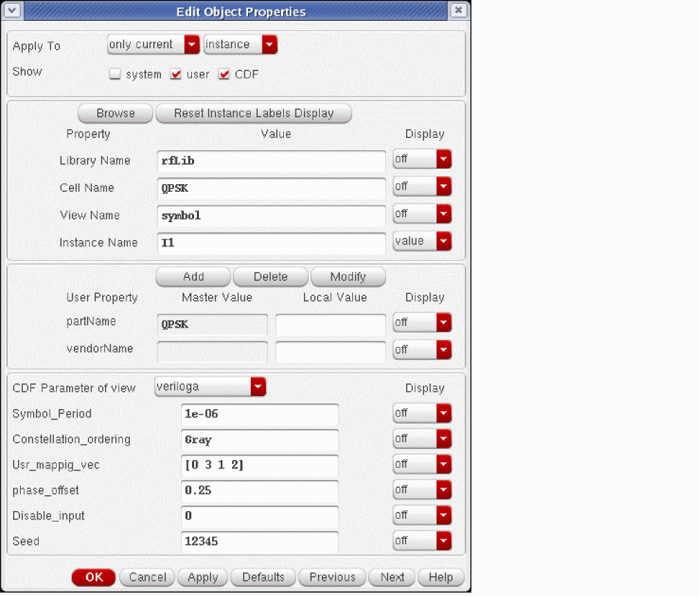
veriloga as the CDF Parameter of view.Figure 1-12 Constellation Map For QPSK
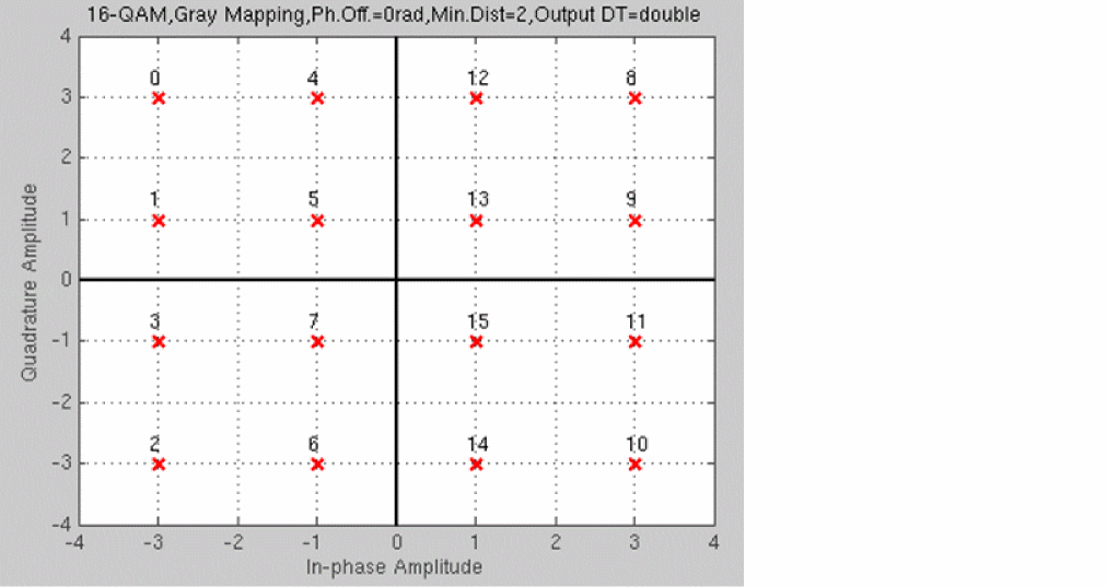
Rectangular_16_QAM
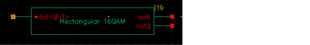
Rectangular_16_QAM takes in a bit signal or generates a pseudo-random bit stream internally and then generates an unfiltered I and Q modulating signal at the output. The number of QAM states is 16 and the output is generated as 16-QAM points separated by the voltages specified by the Dist_or_power property by default.
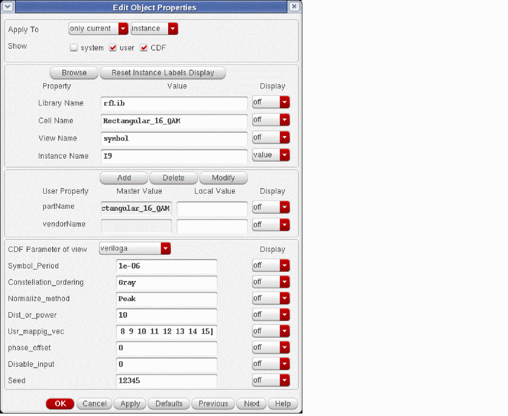
Rectangular_16_QAM block in the schematic capture tool and you use the properties form, select veriloga as the CDF Parameter of view.Figure 1-13 Constellation Map For Rectangular_16_QAM
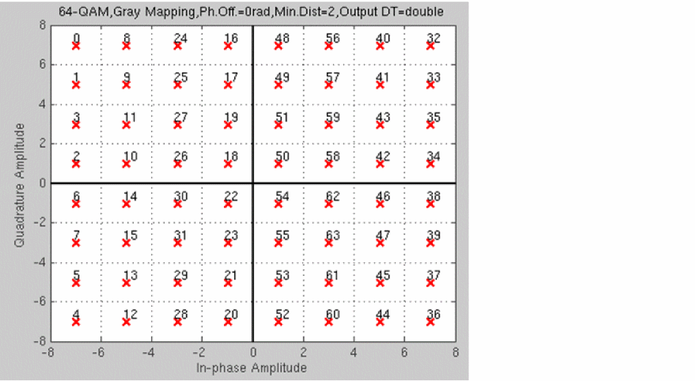
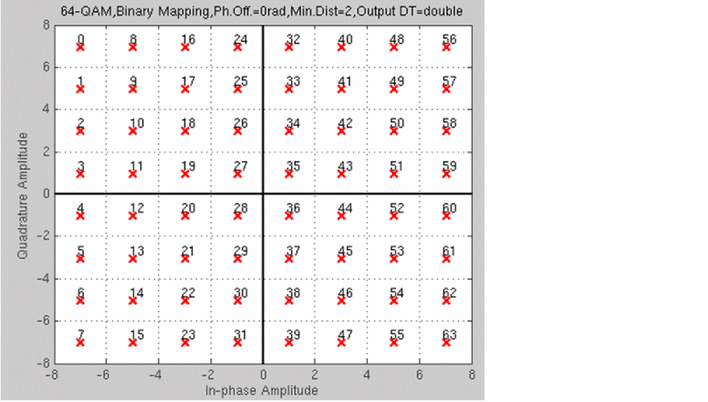
Rectangular_64_QAM
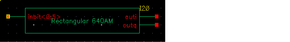
Rectangular_64_QAM takes in a bit signal or generates a pseudo-random bit stream internally and then generates an unfiltered I and Q modulating signal at the output. The number of QAM states is 64 and the output is generated as 64-QAM points separated by the voltages specified by the Dist_or_power property by default.
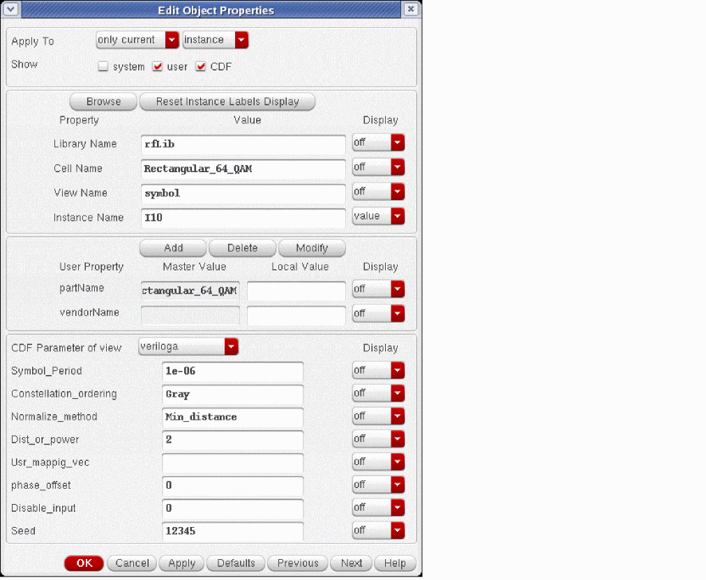
Rectangular_64_QAM block in the schematic capture tool and you use the properties form, select veriloga as the CDF Parameter of view.Figure 1-14 Constellation Map For Rectangualr_64_QAM
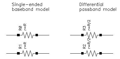
res_BB
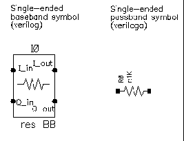
Besides the resistance, the baseband resistor model has a parameter for turning its thermal noise on or off. The baseband resistor is intended for use at a passband node because it’s noise is doubled. (This was discussed in the section entitled “Relationship between baseband and passband noise”). Figure 1-16 shows the symbol, baseband, and passband models. The total noise in the differential passband resistor model equals the noise in one resistor of R Ohms.
rfVsourceBB
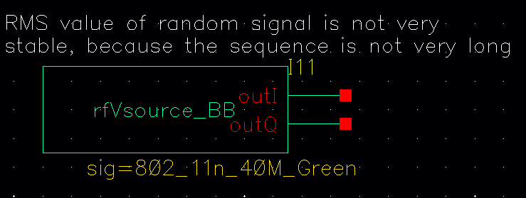
The rfVsourceBB is a baseband signal generator that provides an 802.11 modulated RF I and Q signals for use in a circuit. The bit sequence is a bit short, so this source should not be used to certify the spectral content of your power amplifier. It should be used for a quick idea only.
up_cnvrt
Figure 1-17 Baseband and Passband Mixer Models
up_cnvrt model is a baseband equivalent model of a mixer used to convert from IF to RF. There are some minor differences in the baseband models that depend on whether conversion is up or down. Figures 1-18 shows what the model does.
Figure 1-18 Calculations for up_cnvrt Mixer
VGA_BB
(Variable Gain Amplifier Model)
Only the Baseband view is available.
Figure 1-19 Variable Gain Amplifier Model
Butterworth_filters Category
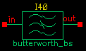
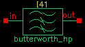
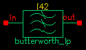
The cells in the Butterworth_filters category are:
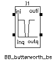
- BB_butterworth_bp
- BB_butterworth_bs
- BB_butterworth_hp
- BB_butterworth_lp
- butterworth_bp
- butterworth_bs
- butterworth_hp
- butterworth_lp
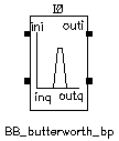
BB_butterworth_bp
For information about the filter parameters, see “BB_butterworth and BB_chebyshev Filter Parameters”.
BB_butterworth and BB_chebyshev Filter Parameters
The parameters for the BB_butterworth and BB_chebyshev filters are:
|
Filter cutoff frequency for lowpass and highpass filter [Hz]. |
|
BB_butterworth_bs
For information about the filter parameters, see “BB_butterworth and BB_chebyshev Filter Parameters”.
BB_butterworth_hp
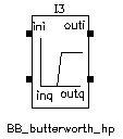
For information about the filter parameters, see “BB_butterworth and BB_chebyshev Filter Parameters”.
BB_butterworth_lp
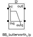
For information about the filter parameters, see “BB_butterworth and BB_chebyshev Filter Parameters”.
butterworth_bp
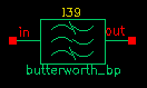
|
Filter cutoff frequency for lowpass and highpass filter [Hz]. |
|
For more information, see “Butterworth and Chebyshev Filter Supporting Information”.
butterworth_bs
|
Filter cutoff frequency for lowpass and highpass filter [Hz]. |
|
For more information, see “Butterworth and Chebyshev Filter Supporting Information”.
butterworth_hp
|
Filter cutoff frequency for lowpass and highpass filter [Hz]. |
|
For more information, see “Butterworth and Chebyshev Filter Supporting Information”.
butterworth_lp
|
Filter cutoff frequency for lowpass and highpass filter [Hz]. |
|
For more information, see “Butterworth and Chebyshev Filter Supporting Information”.
Butterworth and Chebyshev Filter Supporting Information
Filter properties are specified in the frequency domain, but it is not easy for Spectre RF to process frequency-domain data. Spectre RF simulation requires a large signal, time-domain model to simulate filter behavior.
As part of the RF AHDL library, filters are implemented using a network synthesis technique which consists of the following two steps:
- Calculate the normalized low-pass filter prototype, which consists of serial inductors and parallel capacitors
- Perform frequency transformation and scaling to synthesize the frequency responses of the filter type
The synthesized model contains many inductors and capacitors. They are implemented using the integral and differential functions of the Verilog-A language. Insertion loss is added using the S-parameter network technique. This network essentially dampens the signal flow by the specified insertion loss value.
In the current implementation of the Verilog-A language, the order and internal states of the filter cannot be dynamically allocated. You must use the 'define directive in the Verilog-A source code to specify the order. Use S-parameters to test the filters because S-parameters capture the input/output impedance matching.
For example, the Butterworth bandpass filter, butterworth_bp, has the following module declaration:
module butterworth_bp(t1, t2);
    inout t1, t2;
    electrical in, out;
    parameter real r1 = 50 from (0:inf);
    parameter real r2 = 50 from (0:inf);
    parameter real f0 = 1e9 from (0:inf);
    parameter real bw = 0.10 from (0:0.5);
    parameter real fc = 1e9 from (0:inf);
    parameter real loss = 0 from [0:inf);
where t1 and t2 are the input and output nodes, respectively.
|
Corner frequency (3 dB point) for low-pass and high-pass filter [Hz]. |
|
Figure 1-28 is the simple schematic used to test the filter. Two ports are used to obtain the S-parameters.
Figure 1-28 Schematic for Testing Filter Models
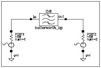
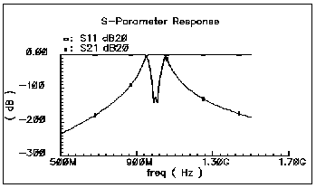
Figure 1-29 shows the calculated S-parameters of this Butterworth bandpass filter, which has a center frequency of 1 GHz and a relative bandwidth of 10 percent. The order of this specific filter is 10.
Figure 1-29 S-Parameters of a Butterworth Filter
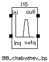
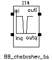
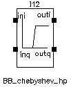
Chebyshev_filters Category
The cells in the Chebyshev_filters category are:
- BB_chebyshev_bp
- BB_chebyshev_bs
- BB_chebyshev_hp
- BB_chebyshev_lp
- chebyshev_bp
- chebyshev_bs
- chebyshev_hp
- chebyshev_lp
BB_chebyshev_bp
For information about the filter parameters, see “BB_butterworth and BB_chebyshev Filter Parameters”.
BB_chebyshev_bs
For information about the filter parameters, see “BB_butterworth and BB_chebyshev Filter Parameters”.
BB_chebyshev_hp
For information about the filter parameters, see “BB_butterworth and BB_chebyshev Filter Parameters”.
BB_chebyshev_lp
For information about the filter parameters, see “BB_butterworth and BB_chebyshev Filter Parameters”.
chebyshev_bp
|
Filter cutoff frequency for lowpass and highpass filter [Hz]. |
|
For more information, see “Butterworth and Chebyshev Filter Supporting Information”.
chebyshev_bs
|
Filter cutoff frequency for lowpass and highpass filter [Hz]. |
|
For more information, see “Butterworth and Chebyshev Filter Supporting Information”.
chebyshev_hp
|
Filter cutoff frequency for lowpass and highpass filter [Hz]. |
|
For more information, see “Butterworth and Chebyshev Filter Supporting Information”.
chebyshev_lp
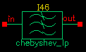
|
Filter cutoff frequency for lowpass and highpass filter [Hz]. |
|
For more information, see “Butterworth and Chebyshev Filter Supporting Information”.
Measurements Category
The measurement category contains elements used to facilitate measurements and diagnostics. Elements in the measurement category can be used by both RF system designers and RF circuit designers.
This section also explains how to change the FIR filters inside the baseband signal generators.
The measurement category contains the following elements, discussed in the sections that follow.
- CDMA_reverse_xmit
- comms_instr
- eye_diagram_generator
- gmsk
- GSM_xmtr
- instr_term
- offset_comms_instr
- pi_over4_dqpsk
- polar_rect
- rect_polar
CDMA_reverse_xmit
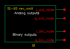
The CDMA signal source (CDMA_reverse_xmit) generates a reverse-link (handset-to-base-station) IS-95 signal with the following characteristics
Two separate 16-bit pseudo-noise generators generate the I and Q spreading sequences operating at the sample rate.
- Generates a random bit at the symbol rate
- Oversamples it by a factor of 4
- Spreads the bit with the I and Q spreading sequences
- Filters each sequence with a 48-tap FIR filter. The filter coefficients are the impulse response of a raised cosine filter.
- Generates a reverse-link (handset-to-base-station) IS-95 signal. The modulation is offset QPSK with a symbol rate of 1.2288 Mega-symbols per second and a sample rate of 4.9152 Megasamples per second. Two separate 16-bit pseudo-noise generators generate the I and Q spreading sequences operating at the sample rate.
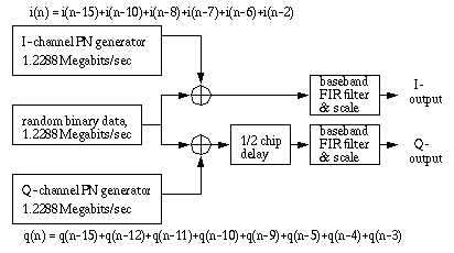
Figure 1-38 shows a block diagram of the signal generator.
Figure 1-38 CDMA Baseband Test Signal Generator
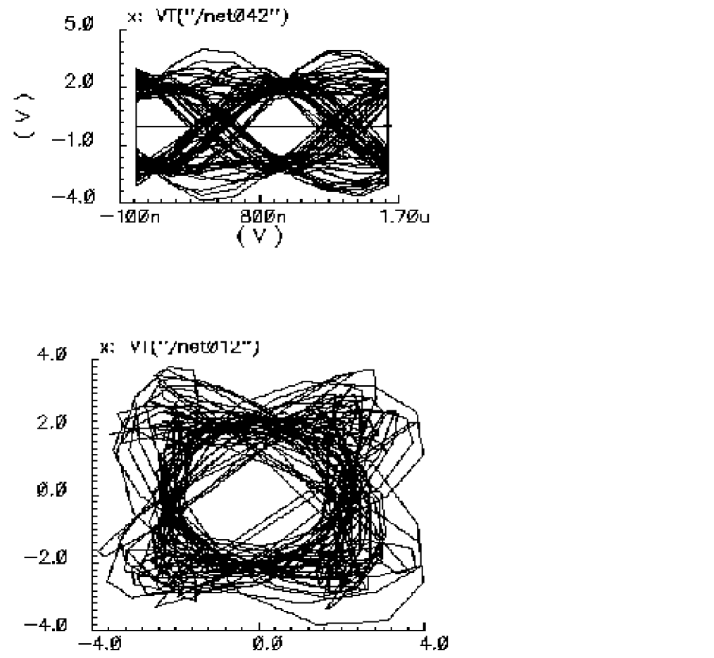
The eye-diagram generator (eye_diagram_generator) created the eye-diagram and trajectory. Figure 1-39 shows the eye-diagram of one of the outputs and the trajectory of both outputs.
Figure 1-39 Eye Diagram and CDMA Trajectory
CDMA Signal Source Instance Parameters
The amplitude parameter sets the amplitude of the unfiltered signals. An amplitude of 1 means that each FIR filter is driven by 1 volt impulses. If you change the internal variable IMPULSE_PULSE to 2, the filters are driven by 1 volt pulses of four samples duration.
The seed parameter changes the seed for the random number generator.
CDMA Signal Source Outputs
The CDMA signal generator creates four output signals:
Changing the FIR Filter in a CDMA Signal Source
You cannot change the FIR filter, such as the tap length and tap coefficients, directly from the instance.
CDMA Signal Source Output Transitions
The filtered outputs slew linearly from one value to the next because the rise and fall times in the transition statements equal one period. To make the outputs take abrupt steps, copy the module to your library and change the rise and fall times in the last transition statements.
comms_instr
The comms_instr block generates waveforms that can be used to create eye-diagrams, eye-diagram statistics, scatter plots, and rms error-vector-magnitudes.
For information about the parameters of the block, see “Instrumentation Block Parameters”. For information about the outputs of the block, see “Instrumentation Block Outputs”. For information about the related offset_comms_instr block, see “(Instrumentation Block)”. For information about the related instr_term block, see “instr_term”.
Figure 1-40 shows how the offset_comms_instr and instr_term blocks should be used. The comms_instr block is used similarly. The circuit consists of two branches driven from a single baseband signal generator. The top branch is the non-ideal receiver model, the bottom branch is an ideal version of the top branch. The ideal version is as ideal as you like. The ideal branch computes ideal symbol locations in the complex plane. The instrumentation block compares ideal and non-ideal symbols to compute the error-vector-magnitude.
Instrumentation Block Parameters
Instrumentation Block Outputs
eye_diagram_generator
The eye-diagram generator creates eye-diagrams and trajectories for the baseband signal generators. For more information, see “Eye-Diagram Generator Input” and “Eye-Diagram Generator Outputs”.
Eye-Diagram Generator Input
The input to the eye-diagram generator is the I or Q output of one of the baseband signal generators.
Eye-Diagram Generator Outputs
The eye-diagram generator has two outputs labeled y-axis and x-axis. The eye-diagram is generated by plotting the y-axis output against the x-axis output.
The eye-diagram generator does not work with Envelope analysis to generate similar plots. This is because the Envelope harmonic time analysis is generated by a post-processing step and the eye-diagram generator works during simulation.
Figure 1-41 shows an eye-diagram of one of the outputs and the trajectory of both outputs for the CDMA baseband signal generator.
Figure 1-41 Example Eye Diagram and CDMA Trajectory
freq_divider
The freq_divider element is a divide by N frequency counter. It contains no hidden state, and it works with SpectreRF. It will fail if N is large, for example, greater than 1000. It reduces tolerances to increase the range of N, or you can split N into integer factors and implement the divide by N with several counters in series.
In release IC 6.1.2 and newer versions, Cadence provides a Verilog-A module for simulating freq_divider behavior. The module is located in rfLib.
-
V(Pin, Nin)must sometimes be greater than zero during the simulation. -
The clocked signal at the input must be larger than threshold; otherwise, the divider might not work properly.
Figure 1-42 freq_divider symbol
The parameters of the instance are listed in the table below:
| Name | Meaning | Range |
gmsk
GMSK (Gaussian minimum shift keying) is a simple but efficient approach to digital modulation that provides the properties of narrow-band techniques, sharp cutoffs in frequency, lower overshoot impulse response, and preservation of the filter output pulse area. These qualities result in low phase distortion and make GMSK suitable for coherent demodulation. The GMSK approach is used in the Global System for Mobile Communication (GSM).
In release IC 6.1.2 and later, Cadence provides a Verilog-A module for simulating GMSK behavior. The module is located in rfLib.
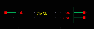
The inbit input supports the use of external random generators. Usually inbit is disabled by specifying enable_input = 0.
The parameters of the instance are listed in the table below:
| Name | Meaning | Type | Default Value | Range |
GSM_xmtr
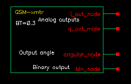
The GSM source generates a signal conforming to the GSM standard. The modulation is GMSK and the data is generated in frames of 3 fixed start bits, 142 random data bits, 3 fixed stop bits, and 8.25 fixed guard bits. (The embedded deterministic pattern and quarter of a bit is necessary to produce the correct spectrum.) The bit rate is 270833.333 bits per second and the sample rate is four times that.
The FIR filter is a Gaussian filter implemented with 32 taps.
Figure 1-44 shows a block diagram of the signal source.
Figure 1-44 GSM Baseband Signal Generator
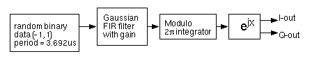
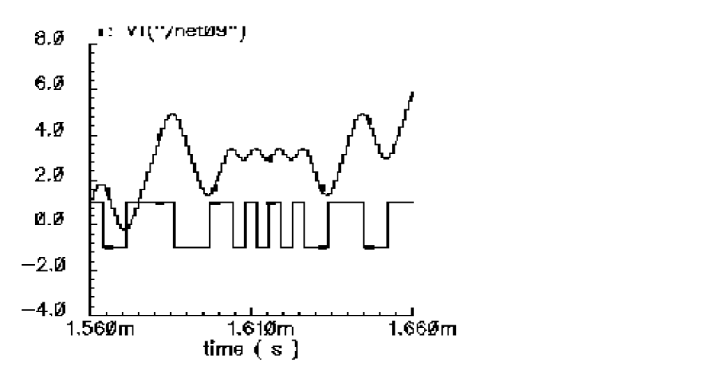
Figure 1-45 shows the binary data stream and the corresponding angle.
Figure 1-45 GSM Binary Data and Resulting Phase
GSM Signal Source Instance Parameters
The amplitude parameter sets the amplitude of the unfiltered signals. An amplitude of 1 means that each FIR filter is driven by 1-volt impulses. If you change the internal variable IMPULSE_PULSE to 2, the filters are driven by 1-volt pulses of four samples duration.
The seed parameter changes the seed for the random number generator.
GSM Signal Source Outputs
The generator creates four output signals:
Changing the FIR Filter in a GSM Signal Source
You cannot directly change the FIR filter, such as the tap length and tap coefficients, from the instance.
GSM Signal Source Output Transitions
The filtered outputs slew linearly from one value to the next because the rise and fall times in the transition statements equal one period. To make the outputs take abrupt steps, copy the module to your library and change the rise and fall times in the last transition statements.
instr_term
The instr_term block simply loads all instrumentation output pins with 50 Ohms. The instr_block keeps the schematic editor from complaining about unconnected pins, nothing more.
For information about the parameters of the block, see “Instrumentation Block Parameters”. For information about the outputs of the block, see “Instrumentation Block Outputs”. For information about the related comms_instr block, see “(Instrumentation Block)”. For information about the related offset_comms_instr block, see “gmsk”.
Figure 1-46 shows how the offset_comms_instr and instr_term blocks should be used. The comms_instr block is used similarly. The circuit consists of two branches driven from a single baseband signal generator. The top branch is the non-ideal receiver model, the bottom branch is an ideal version of the top branch. The ideal version is ideal as you like. The ideal branch computes ideal symbol locations in the complex plane. The instrumentation block compares ideal and non-ideal symbols to compute error-vector-magnitude.
offset_comms_instr
The offset_comms_instr block generates waveforms that can be used to create eye-diagrams, eye-diagram statistics, scatter plots, and rms error-vector-magnitudes.
The offset block is identical to the comms_instr except that the sampling time for scatter plots and eye-diagram statistics are delayed by half a symbol period. The delay makes it possible to plot symbols in an offset QPSK modulation scheme.
For information about the parameters of the block, see “Instrumentation Block Parameters”. For information about the outputs of the block, see “Instrumentation Block Outputs”. For information about the related comms_instr block, see “(Instrumentation Block)”. For information about the related instr_term block, see “instr_term”.
Figure 1-47 shows how the offset_comms_instr and instr_term blocks should be used. The circuit consists of two branches driven from a single baseband signal generator. The top branch is the non-ideal receiver model, the bottom branch is an ideal version of the top branch. The ideal version is as ideal as you like. The ideal branch computes ideal symbol locations in the complex plane. The instrumentation block compares ideal and non-ideal symbols to compute error-vector-magnitude.
pi_over4_dqpsk
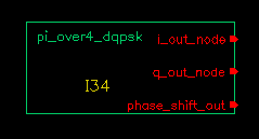
Figure 1-48 shows the block diagram for this source.
Figure 1-48 Π/4-DQPSK baseband signal generator
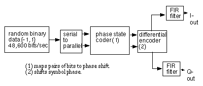
Table 1-49 shows how the phase shift is generated.
| 1st bit | 2nd bit | Phase shift |
|---|---|---|
The symbol rate is 24300 symbols per second and the sample rate is 8 times that. The FIR filter is a raised cosine filter implemented with 64-taps.
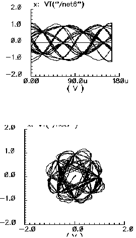
The eye-diagram generator (eye_diagram_generator) created the eye-diagram and trajectory. Figure 1-50 shows the eye-diagram and trajectory for this generator.
Figure 1-50 Eye Diagram and Pi/4 Trajectory
The amplitude parameter lets you set the amplitude of the unfiltered signals. An amplitude of “1” means that each FIR filter is driven by 1-volt impulses. If you change the internal variable IMPULSE_PULSE to 2, the filters are driven by 1-volt pulses of four samples duration.
The seed parameter lets you change the random number generator seed.
Pi/4-DQPSK Signal Source Outputs
The generator creates three output signals.
Changing the FIR filter in a Pi/4-DQPSK Signal Source
You cannot change the FIR filter, such as the tap length and tap coefficients, directly from the instance.
Pi/4-DQPSK Signal Source Output Transitions
The filtered outputs slew linearly from one value to the next because the rise and fall times in the transition statements equal one period. To make the outputs take abrupt steps, copy the module to your library and change the rise and fall times in the last transition statements.
polar_rect
(Polar-to-Rectangular Transformation)
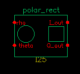
The polar-to-rectangular block is in the measurement category. The only parameters are input and output resistances. The inputs are the baseband signal in polar coordinates, the outputs are the baseband signal in rectangular coordinates.
rect_polar
(Rectangular-to-Polar Transformation)
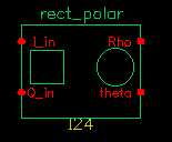
The rectangular-to-polar block is in the measurement category. The only parameters are input and output resistances. The inputs are the baseband signal in Cartesian coordinates, the outputs are the baseband signal in polar coordinates.
Parameters: Input and output resistances.
where θ is in radians and with appropriate checks for the i = 0 case
Passband_components Category
The Passband_components category contains the following elements, discussed in the sections that follow.
IQ_demodulator
Figure 1-51 Baseband and Passband IQ Demodulator Models
The IQ_demodulator converts RF (or IF) to baseband. Figure 1-52 shows exactly what the passband demodulator model does. The parameters are like those in the modulator blocks except saturation is specified by input referred IP3 instead of by 1 dB compression point. IP3 was chosen over the 1 dB compression point for specifying saturation because the demodulator usually lies in the receive path and receiver blocks are usually specified with IP3.
Figure 1-52 IQ Demodulator Calculations
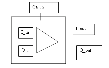
IQ_modulator
Figure 1-53 Baseband and Passband IQ Modulator Models
The IQ_modulator converts baseband signals to RF or IF. Figure 1-54 summarizes exactly what the passband IQ modulator model does. The only difference between the baseband and passband models is carrier suppression. The non-linear functions, gi and gq, are specified by their available power gain and 1dB compression points just as in the power amplifier. The functions γi and γq characterize AM/PM effects in each mixer and are specified by the same parameters that specify power amplifier AM/PM conversion. Because noise is always added at the input, and the input is at baseband in this case, the noise sources are not doubled as they are in the power amplifier or LNA models. Noise figure is defined with reference to one input. Noise is injected at both inputs but the noise injected at just one input alone produces the specified noise figure. Thus, the noise figure parameter should be interpreted as noise figure per input. This model also includes a parameter called quadrature error which specifies how far away the two local oscillators signals are from being exactly in quadrature.
Phase error is the voltage on the phase error pin. The phase error pin has a fixed noiseless resistive input impedance of 50 ohms. The phase error pin can be used to introduce a dynamic phase error or phase noise. Phase noise can be fed into the phase error pin from a phase-domain PLL model or from a Port. Noise in Port models can be specified either by the internal resistance or by a data file that tabulates a power spectral density. The phase error pin can also be driven by a ramp or circular integrator output to model a frequency error between the incoming carrier and local oscillator.
The following parameters specify the IQ modulator. The available power gain and one dB compression point are explained first. The effects of the phase_error pin and the quadrature error parameter are discussed at the end of this section.
Figure 1-54 IQ Modulator Calculations
LNA_PB
Figure 1-55 Baseband and Passband Power Amplifier Models
The following parameters specify the low noise amplifier model.
MIXER_PB
Figure 1-56 Baseband and Passband Mixer Models
MIXER_PB is a passband model that converts RF to IF and IF to RF.
PA_PB
shifter_combiner
The shifter_combiner combines two signals so that they add if one leads the other by 90 degrees and so that they cancel if it lags by 90 degrees.
shifter_splitter
The shifter_splitter splits a signal into two signals 90 degrees out of phase with each other.
RF_components Category
The cells in the RF_components category are:
- ACPR_source
- balun
- balun_com
- gfsk
- lna
- mixer
- ofdm
- osc
- pa
- quadrature
- RFVsource
- shifter
- Triplexer
- Ten_plexer
ACPR_source
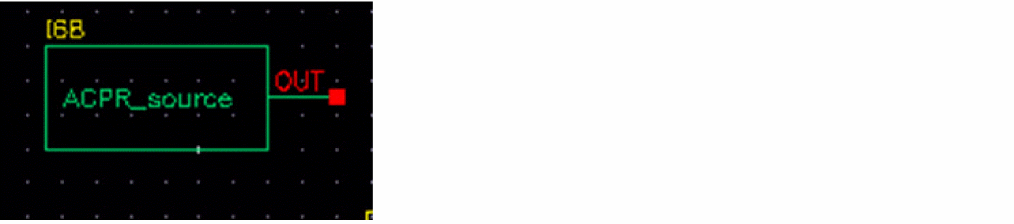
The ACPR_source is used to generate modulated RF waveforms. It is a self-contained RF modulator. The out connection is the modulated RF output.
balun
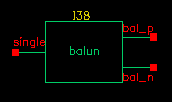
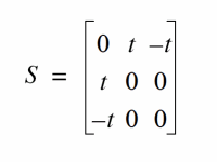
The balun (balancing transformer) is used in circuits that require single/differential signal transformation. Although a passive network (including the transformer) is used to achieve balun, this implementation employs a three-port network. There are three ports (or nodes), because the reference nodes are always at the global ground: single, bal_p, and bal_n.
When the ports are numbered as single(1), bal_p(2), and bal_n(3), the S-parameter for the three-port network is
This module can also be used in common mode cancellation applications.
The module is declared as follows
module balun(single, bal_p, bal_n);
  inout single, bal_p, bal_n;
  electrical single, bal_p, bal_n;
   parameter real rin = 50 from (0:inf);
   parameter real rout = 50 from (0:inf);
   parameter real loss = 0 from [0:inf);
Parameters include the input impedance (for single end), the output impedance (for balanced end to ground), and the insertion loss (from single end to balanced end and from balanced end to single end).
balun_com

The balun_com has, in addition to the three ports of the balun, an external reference node that can be used for DC bias set up in the balanced end. The balun_com is equivalent to the balun when the voltage of the reference node c is set to 0.
The four ports of the balun_com are:
The module is declared as follows
module balun_com(s, p, n, c);
  inout s, p, n, c;
  electrical s, p, n, c;
   parameter real rin = 50 from (0:inf);
   parameter real rout = 50 from (0:inf);
   parameter real loss = 0 from [0:inf);
Parameters include the input impedance (for single end), the output impedance (for balanced end to ground), and the insertion loss (from single end to balanced end and from balanced end to single end).
gfsk
(Gaussian-filtered frequency shift keying I and Q modulation generator)
GFSK is a Gaussian filtered frequency modulation I and Q signal generator, which makes the I and Q output smoother so as to limit the spectral width. GFSK is poorer in terms of the spectral efficiency but easier to implement as compared to GMSK. GFSK is often seen in cordless phones using the DECT standard and in bluetooth.
The symbol connection ports are:
|
Inbit is a connection for an external random bit stream. This connection is enabled when the |
|
Instance Parameters
lna
Low-noise amplifiers (LNAs) are commonly used in receiver designs to amplify the signal with a low noise figure. A typical LNA has the following three sets of parameters:
The module is declared as follows:
module lna(in, out);
   inout in, out;
   electrical in, out;
   parameter real nf = 2 from [0:inf);
   parameter real ip3 = -10;
   parameter real gain = 15 from [0:inf);
   parameter real isolation = 200 from (0:inf);
   parameter real rin = 50 from (0:inf);
   parameter real cin = 0 from [0:100];
   parameter real rout = 50 from (0:inf);
   parameter real cout = 0 from [0:100];
   parameter real gammain = -150 from (-inf:0];
   parameter real mismatch = 1 from [-1:1] exclude (-1:1);
   parameter real gammaout=-150 from (-inf:0];
cin and cout.|
Mismatch sign of input. 1: input impedance > reference |
|
Internally, a set of linear equations is constructed to satisfy the S-parameters. Furthermore, nonlinearity, expressed by a third-order polynomial function, is added to the gain (or S21) to describe the IP3. Excess white noise is added at the input port to describe the noise figure.
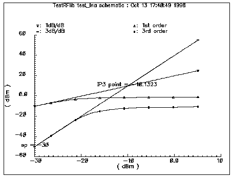
IP3 is the measure of the corruption of signals due to the third-order intermodulation of two nearby tones as shown in Figure
Figure 1-57 Intermodulation of Two Nearby Signals
Figure 1-58 shows the captured IP3 when the requested value of IP3 is −10dBm.
Figure 1-58 IP3 from Spectre RF Simulation
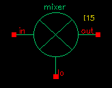
mixer
Mixers are important for frequency translation in RF circuits. A typical mixer has the following three sets of parameters.
This RF library model describes the typical behavior of integrated mixers. The LO switches the input signal on and off. Input LO power beyond the specified limit is effectively clipped off.
module mixer(in, lo, out);
    electrical in, lo, out;
    parameter real gain = 10 from [-50:50];
    parameter real plo = 10 from [-100:100];
    parameter real rin = 50 from (0:inf);
    parameter real rout = 200 from (0:inf);
    parameter real rlo = 50 from (0:inf);
    parameter real ip2 = 5;
    parameter real ip3 = 5;
    parameter real nf = 2 from [0:inf);
    parameter real isolation_LO2IN = 20 from (0:inf);
    parameter real isolation_LO2OUT = 20 from (0:inf);
    parameter real isolation_IN2OUT = 20 from (0:inf);
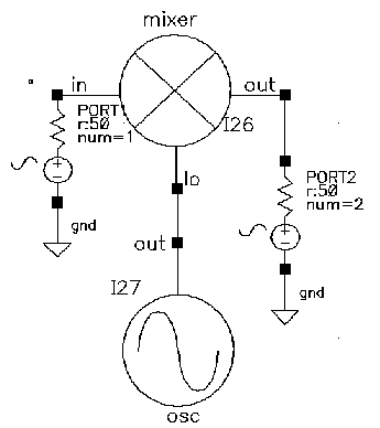
Figure 1-59 is the simple schematic that tests the mixer.
Figure 1-59 Schematic for Testing the Mixer Model
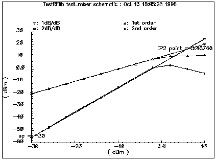
The maximum power of the fundamental frequency of the local oscillator, plo, can be used in the mixing process. Therefore, the gain, defined as the output power of the mixed product versus the input power of the RF signal, depends on the power level of the LO. The gain levels off, however, to the specified maximum value as the LO signal becomes larger.
You can measure both IP3 and IP2 with Spectre RF. You must select frequencies carefully when you measure IP3 to measure harmonic distortion (HD) and IP2. Testing IP3 requires two tones to measure the intermodulation distortion (IMD), while testing IP2 requires only one tone.
Assume the RF input frequencies are f1 and f2, and the LO frequency is flo. If the input power level at f1 equals that at f2, the IP3 is the intercept point of the extrapolated line of output power at frequency |flo - (2f2 - f1)| versus the extrapolated line of the linear output signal at |flo-f1|. Input-referenced IP3, therefore, can be read as the X-axis value at the intercept point. The IP2, for the purpose of measuring the half-IF effects, is defined as the intercept point of the extrapolated line of output power at frequency | 2 ( f lo - f 1)| versus the linear output signal. Figure 1-59 shows that the intercept point of the 1 dB/dB and 2 dB/dB lines is at the X-axis reading of 4.78 dBm, while the requested IP2 value is 5 dBm. The order of the intercept point is based only on the order of the RF signals. The order of LO signal is not counted in the definition of the intercept point. In the implementation of this model, the orders of LO for IP3 and IP2 are 1 and 2 respectively.
Internally, a set of equations is built to satisfy a three-port S-parameter. A third-order polynomial describes the nonlinearity of IP3. The LO signal is further multiplied by itself to derive the second-order harmonic, which is then used to produce the IP2 effect. Excessive white noise is added in the RF input port to satisfy the noise figure. Remember, however, that the noise figure is double-sideband. If the noise at the image frequency is not filtered out, the measured noise figure is 3dB larger than the DSB noise figure.
ofdm
(Orthogonal Frequency-Division Multiplexing)
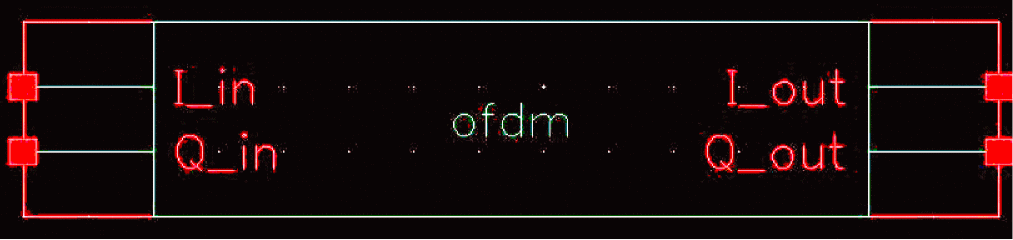
OFDM is a digital multi-carrier modulation scheme, in which closed-spaced sub-carriers are summed into main carrier. These sub-carriers are orthogonal to each other and modulated with conventional modulation scheme at a low symbol rate. The summation is performed through Fast Fourier Transform.
OFDM has the merit of robost against intersymbol interference and narrow-band co-channel interference. It is spectral-efficient. It has seen many applications such as WiMAX, MBWA, Wi-Fi and UWB and so on.
|
Input signals, activated only when “input_enable” is set to 1. |
|
Instance Parameters
|
The length of vector for shift register's feedback connections |
|
osc
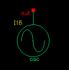
Oscillator models describe the essential information for a typical oscillator, more precisely, a local RF power source.
The definition of the model in the Verilog-A language is as follows:
module osc(out);
    electrical out;
    inout out;
    parameter real power = 10;
    parameter real f = 1e9 from (0:inf);
    parameter real rout = 50 from (0:inf);
    parameter real floor = -60 from (-inf:0);
    parameter real f1 = 1000 from (0:1e6);
    parameter real n1 = -40 from (bottom:0);
    parameter real fc = 0 from [0:f1);
This model is not an autonomous model. Rather, it simply generates a sinusoidal wave with the specified impedance, power level, and phase noise characteristics.
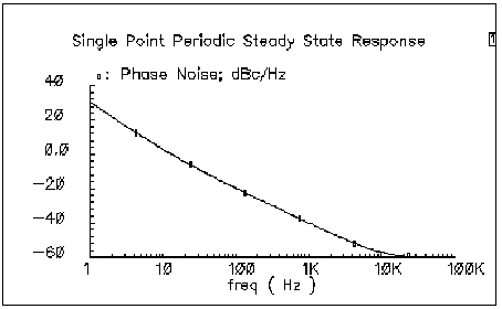
When the load is matched to the internal impedance, the load dissipates the specified output power. You can specify the noise floor of the output signal. Furthermore, by adding one point (frequency, phase noise), you can specify 1/ f 2 frequency noise (corresponding to the phase noise induced by white noise). If f c, the corner frequency of white phase and flicker phase noise, is bigger than 0, 1/ f 3 frequency noise (flicker-noise-induced phase noise) is further specified. Otherwise, 1/ f 3 noise is not included.
The phase noise values that are symmetric around the carrier are correlated. The noise floor, however, is not correlated.
Figure 1-60 shows the phase noise of the oscillator model. In Figure 1-60, the specified parameters are:
Figure 1-60 Phase Noise for the Oscillator
pa
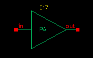
Power amplifiers (PAs) are used in RF transmitters to achieve output of a higher power level. The PA model differs from the LNA model in that it has greater power delivery capabilities with less stress on matching capabilities.
The Verilog-A module is declared as follows:
module pa(in, out);
    inout in, out;
    electrical in, out;
    parameter real nf = 2 from [0:inf);
    parameter real gain = 20 from [0:inf);
    parameter real rin = 50 from (0:inf);
    parameter real rout = 50 from (0:inf);
    parameter real p1db = 30;
    parameter real psat = 35;
    parameter real ip2 = 40;
The power amplifier model has the following three parts:
Internally, for simplicity, the reverse isolation is assumed to be ideal. A set of linear equations is constructed to satisfy these S-parameters. Nonlinear effects are added to the gain to describe the nonlinearity. The output power of the power amplifier compresses to 1 dB less than the output of an ideal linear amplifier at the 1 dB compression point. Further increase of the input power makes the output approach the saturation power only at the fundamental operating frequency. IP2 describes the second order effects of the amplifier, so use only one tone in the test. Excess white noise is added at the input port to describe the noise figure.
The implementation of psat assumes a pure sinusoidal waveform. To maintain a restrained output power, the output waveform is clipped from a sinusoidal to a square wave form. Figure 1-61 shows the input and output waveforms of the power amplifier. Because of the output waveform clipping, the input sinusoidal wave should have a DC component of zero.
Figure 1-61 Input and Output Waveforms of the Power Amplifier
Figure 1-62 shows the 1 dB compression point and the saturation power. This difference is caused by the 50 Ω load impedance. The specified output referenced 1 dB compression point is 40 dBm, which Spectre RF captures as 39.6.
If psat is much larger than p1db, your psat might not be satisfied.
Figure 1-62 1dB Compression Point and Saturation Power
quadrature
The quadrature signal generator model is included because, in quadrature receiver design, a phase shifter is ordinarily used to generate the quadrature signal from one signal source such as the VCO. However, a phase shifter is hard to implement in a wide band model.
A quadrature signal consists of two signals with a 90-degree phase difference but with identical noise and amplitude.
The Verilog-A module is declared as follows.
module quadrature(lead, lag);
    electrical lead, lag;
    inout out_cos, out_sin;
    parameter real power = 10;
    parameter real f = 1e9 from (0:inf);
    parameter real rout = 50 from (0:inf);
    parameter real floor = -60 from (-inf:0);
    parameter real f1 = 1000 from (0:1e6);
    parameter real n1 = -40 from (bottom:0);
    parameter real fc = 0 from [0:f1);
The difference between the quadrature signal generator model and the oscillator model is that the oscillator has only one output node but the quadrature signal generator has two output nodes, lead and lag. In the quadrature signal generator model, when the power levels, output impedances, and noise sources are identical, the two outputs, lead and lag, have a 90-degree phase difference.
RFVsource
(RF modulated source for 802.11 standards)
The rfVsource is a full RF signal generator that provides an 802.11 modulated RF signal for use in a circuit. The bit sequence is a bit short, so this source should not be used to certify the spectral content of your power amplifier. It should be used for a quick idea only.
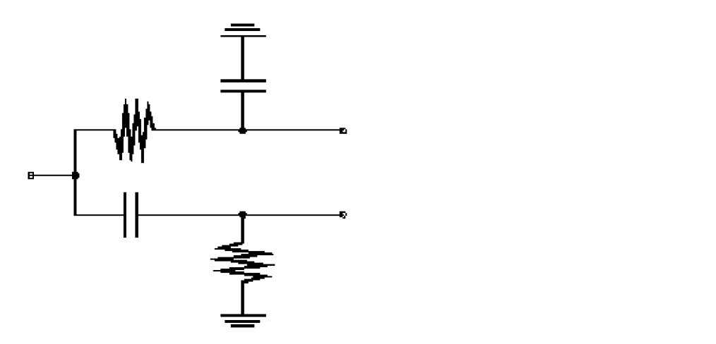
shifter
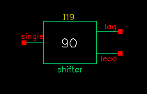
In digital RF system designs, quadrature signal processing involves the phase splitting of high-frequency signals. The most common use of such components is to generate two signals that have a 90-degree phase difference based on one signal source (such as the RF signal or oscillator output). Another common use for a phase shifter is to combine two signals after adding a 90-degree phase difference, as in image-rejection receiver designs.
The Verilog-A module is declared as follows
module shifter(single, lag, lead);
    inout single, lag, lead;
    electrical single, lag, lead;
    parameter real freq = 1e9 from (0:inf);
    parameter real r    = 50 from (0:inf);
|
Resistance [Ω] (see Figure 1-63). |
Internally, the phase shifter is implemented using the RC-CR circuit as shown in Figure 1-63. While the phase difference is also 90-degrees when the lead and lag have the same output impedance, only at the operating frequency do the magnitudes remain the same. This circuit network also generates white noise.
There are two buffered versions of the shifter:
-
The
shifter_combinercombines two signals so that they add if one leads the other by 90 degrees and so that they cancel if it lags by 90 degrees. -
The
shifter_splittersplits a signal into two signals 90 degrees out of phase with each other. - You specify the input and output impedances. These networks are noiseless.
Triplexer
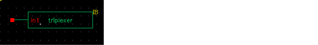
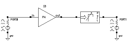
The triplexer is a series of three Bessel filters followed by three portAdapters and three ports. Bessel filters are chosen because there is no ripple in the passband of the filter and the transient response is not complicated. This allows a tstab to be set in the simulation to allow the filters to reach steady-state.
This is done to allow different reflection coefficients at the first three harmonics of the output frequency for a loadpull analysis on a power amplifier. Note that the output port is inside the triplexer schematic. To plot the loadpull, open-read the triplexer schematic and probe the terminal of the topmost port on the right side of the circuit.
The bandpass filters must be kept quite narrow in order to minimize the interactions between the filters in the triplexer schematic. The bandwidth is set as a percentage of the frequency of the first filter.
The schematic of the triplexer is shown below.
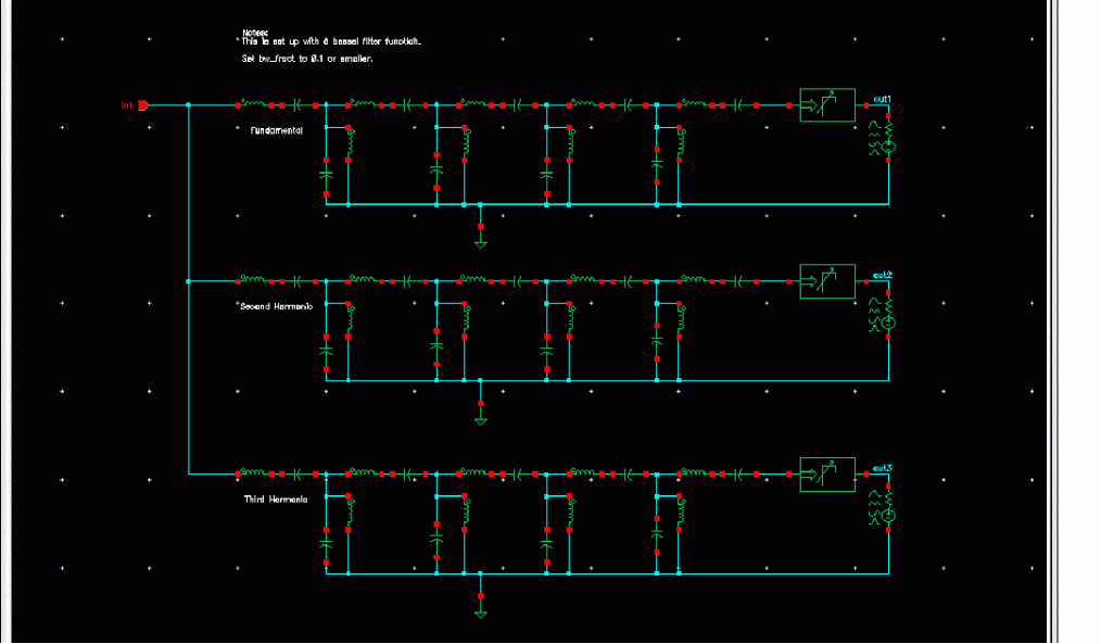
If you wish to change the filter type, you can do so by copying the triplexer cell into a local library and editing the schematic. You can then edit the properties of the components. The first number of the numerator or denominator is the one radian per second and 1 ohm value you can find in any filter design manual. If you have a choice, put the largest values in the leftmost component of the filter. When the value for the leftmost inductor is less than the default of 2.2649, the bw_fract should be reduced in order to prevent interaction between the filters.
Ten_plexer

The ten_plexer is a series of ten Bessel filters followed by ten portAdapters and ten ports. Bessel filters are chosen because there is no ripple in the passband of the filter and the transient response is not complicated. This allows a tstab to be set in the simulation to allow the filters to reach steady-state.
This is done to allow different reflection coefficients at the first ten harmonics of the output frequency for a loadpull analysis on a power amplifier. Note that the output port is inside the ten_plexer schematic. To plot the loadpull, open-read the ten_plexer schematic and probe the terminal of the topmost port on the right side of the circuit.
The bandpass filters must be kept quite narrow in order to minimize the interactions between the filters in the ten_plexer schematic. The bandwidth is set as a percentage of the frequency of the first filter.
The schematic of the ten_plexer is shown below.
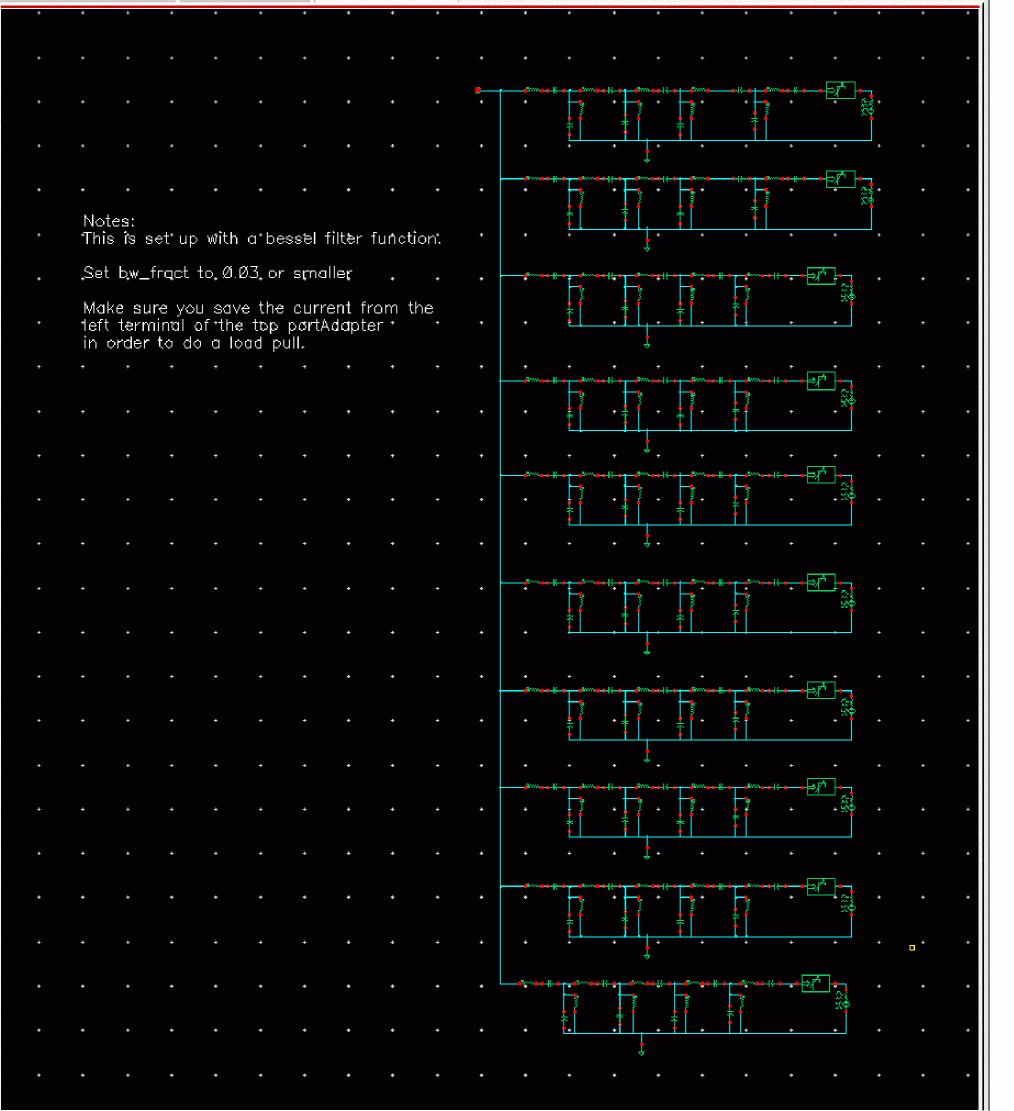
If you desire to change the filter type, you can do so by copying the ten_plexer cell into a local library, and editing the schematic. You can then edit the properties of the components. The first number of the numerator or denominator is the one radian per second and 1 ohm value you can find in any filter design manual. If you have a choice, put the largest values in the leftmost component of the filter. When the value for the leftmost inductor is less than the default of 2.2649, the bw_fract should be reduced in order to prevent interaction between the filters.
Testbenches Category
The testbenches category contains the test circuits used to define model specifications. Where possible, the element names are in terms of standard RF measurements. The most precise way to describe a measurement is with a test circuit, set up instructions, and sample measurements. The circuits in the testbenches category serve this purpose.
The components in the testbenches category are:
- AM_PM_test_ckt
- ava_pwr_gain
- BB_ind_cap_test
- demod_ip3
- dwn_cnvt_test
- mixer_ip3
- mod_1dbcp
- mod_demod_test
- noise_figure
- one_db_cp
- PB_BB_filter_comparison
- PB_ind_cap_test
- quad_and_phase_error_demo
- shifter_combiner_test
- shifter_splitter_test
- up_cnvt_test
- view_switching
AM_PM_test_ckt
Only the baseband models include the four parameters for AM/PM conversion.
The test circuit in Figure 1-64 is listed as am_pm_test_ckt in the testbenches category in rfLib.
Figure 1-64 The am_pm_test_ckt Circuit
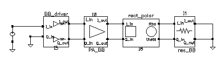
In the am_pm_test_ckt test circuit,
-
The first block (
BB_driver) scales the control voltage generated by the leftmost element so that the output equals the specified dBm when the control voltage equals 1 volt. This is done so you can specify maximum dBm but still sweep linearly from zero signal. -
The second block (
PA_BB) is a power amplifier. -
The third block (
rect_polar)transforms the rectangular description of the baseband signal into polar coordinates so you can observe the phase shift and output signal level directly.
Figure 1-65 shows the output amplitude and phase as functions of the input signal level. Generate these with a swept DC analysis. Sweep the signal variable from 0 to 1 in 200 linear steps and display the rect_polar outputs.
Figure 1-65 Output Amplitude and Phase
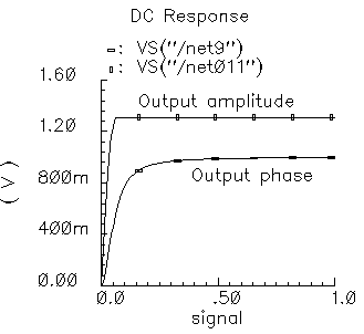
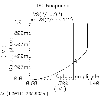
By changing the x-axis to be the output amplitude trace, you can confirm that the phase shift at the output referred 1 dB compression point of 10dBm (or 1 volt peak across a 50 ohm load) equals 0.3 radians, as specified. Figure 1-66 shows the plot.
Note that the measured power across the load is as specified only when the load matches the amplifier output resistance. If you mismatch the load you do not measure the specified phase shift at the specified output power level.
Figure 1-66 Output Phase Versus Output Amplitude
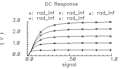
In the next three figures, output phase is plotted against input signal level. Each plot shows the effect of one of the AM/PM conversion parameters. You can generate the plots by applying the Parametric Tool to the existing analysis.
Figure 1-67 shows the effect of the |radians|@1 db cp parameter. Sweep rad_cp from 10 m to 100 m in 5 linear steps.
Figure 1-67 Output Modified by the |radians|@1 db cp Parameter
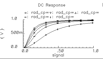
Figure 1-68 shows the effect of the am/pm sharpness parameter. Sweep sharpness from 1 to 6 in 5 linear steps.
Figure 1-68 Output Modified by the Sharpness Parameter
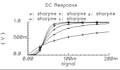
Figure 1-69 shows the effect of the rad_inf parameter. Sweep rad_inf from 0.5 to 3 in 5 linear steps.
Figure 1-69 Output Modified by the rad_inf Parameter
ava_pwr_gain
(Available Power Gain Parameter)
When an amplifier’s load is equal to it’s output resistance, available power gain equals the following
The test circuit in Figure 1-70 is listed as ava_pwr_gain in the testbenches category in rfLib.
Figure 1-70 The ava_pwr_gain Circuit
Computing Constant Power Contours
The ava_pwr_gain test circuit is set up to compute constant power contours. As you would expect, maximum power transfer occurs when the load and output impedances are matched. The port adapter inserts reactive elements into the signal path to load the amplifier with the specified reflection coefficient.
Figure 1-71 shows a Smith Chart that displays how the load power varies with the load refection coefficient.
The load pull contours were computed by
-
Sweeping the
ppparameter in a PSS analysis (ppis the phase of the reflection coefficient) -
Sweeping the
mmparameter with the Parametric Tool (mmis the magnitude of the reflection coefficient)
The load reflection coefficient is defined with reference to the amplifier output resistance, 300 Ohms in this case. The amplifier input resistance is 20 Ohms. The input source resistance is 50 hms. The amplifier 1 dB compression point is set high enough to make the amplifier linear. The available power gain parameter is 20 dB.
To generate the load pull contours you must save both the current flowing into the port adapter (port) and the current flowing into Port0.
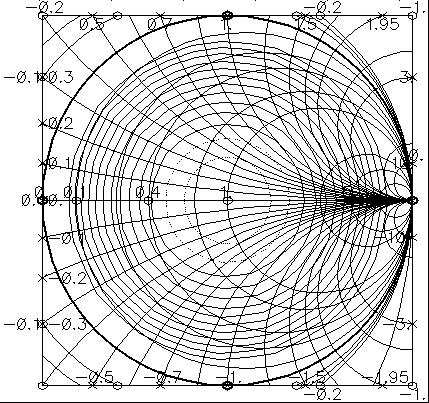
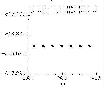
When you place the cursor on the smallest contour on the Smith Chart, you can see that the amplifier delivers a maximum power of 81.63 mW to an optimum load of 300 Ohms (reflection coefficient = 0). When you plot the magnitude of the power coming from the input port against the sweep variable (pp, phase of the reflection coefficient) you find that input power equals 816.3 uW, independent of load, as shown in Figure 1-72. The ratio of maximum output to input power equals 100, or dB, as specified.
Note that the voltage gain in this test circuit does not equal 10 because the amplifier’s input and output resistances are different. You can verify that the ratio of the output to input voltage is as follows
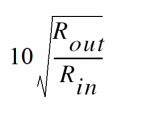
where, Rout is the amplifier output resistance and Rin is the amplifier input resistance. This assumes the amplifier is not driven into non-linear operation.
The input and output resistances specify the current drawn by the associated terminals as a linear function of terminal voltage. There is no test circuit for terminal resistances because the definition is so simple.
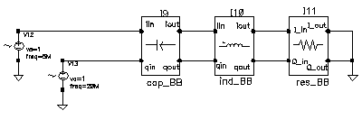
BB_ind_cap_test
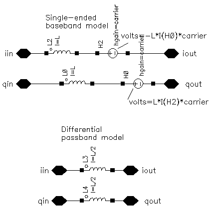
The two circuits discussed below demonstrate how passband and baseband reactive elements are related. The circuit in Figure 1-73 shows a simple passband RLC circuit driven by a modulated carrier. The circuit in Figure 1-74 shows the associated baseband equivalent circuit model. The circuits are PB_ind_cap_test and BB_ind_cap_test. Both circuits reside in the rfLib under the testbenches category.
Figure 1-73 Simple Passband RLC Circuit
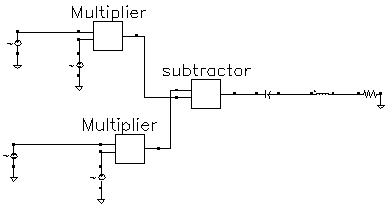
Figure 1-74 Baseband Equivalent To Figure 1-63
The following steps explain how to simulate each circuit and overlay the results.
-
Recall the
PB_ind_cap_testcircuit and bring up an analog design environment window. Set up a 200 ns Envelope analysis. Selectcarrieras the Clock Name. Set the Output Harmonics to 1. -
Run the analysis and plot the real and imaginary parts of the harmonic-time voltage across the resistor. Use
1for the harmonic number. -
Recall the
BB_ind_cap_testcircuit and run a 200 ns transient analysis. Note the faster run time. That is the whole point to suppressing the carrier but it is only useful if the results match. Plot theI_inandQ_involtages of the resistor model. - To overlay the results, bring up a waveform calculator.
- Click the wave button on the calculator then click one of the Envelope waveforms. If the waveform turns yellow you may have to hit the escape button a few times and click clear and clst a couple of times in the calculator then try again.
- Make active the waveform display tool with the transient results then click Plot in the calculator.
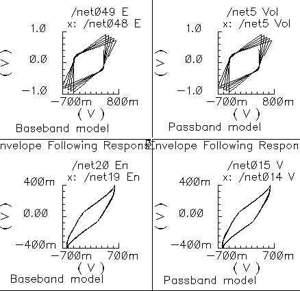
- Repeat the last two steps for the other Envelope waveform. You should see the waveforms in Figure 1-75. The two models agree very well. The resonant frequency of the series RLC branch is just over 500 MHz. Only by riding on a carrier can the 5 MHz and 20 MHz baseband signals propagate to the resistor at their original voltage levels. The baseband model accurately predicts the effects of the RLC circuit on the baseband signal. There are two effects, one due to phase shift at the carrier frequency and one due to filtering of the baseband signal itself.
-
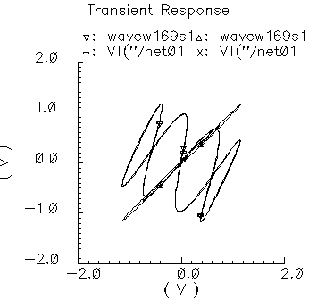
In the waveform display tool that overlays the results, change the x-axis to be one of the I-signals. You should get the picture shown in Figure 1-76. The tilt in the resulting Lissajous plot indicates phase shift at the carrier frequency but not at the baseband frequencies. The aspect ratio of the Lissajous figure indicates the 20 MHz component is attenuated more than the 5 MHz component. The baseband model captures both effects well.
Figure 1-75 WaveformsFigure 1-76 Lissajous plot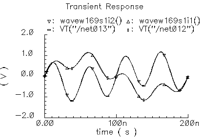
Comparison of Baseband and Passband Models
The circuit in Figure 1-77 shows how well the baseband and passband filters agree. The I-input is a 5MHz 1 volt peak sinusoid and the Q-input signal is a 20MHz 1 volt peak signal. The filter has a center frequency of 1.1GHz and a relative bandwidth of 0.1. The modulator LO is 1GHz. To make the analysis more interesting the carrier is not exactly aligned with the filter center frequency and the terminals are not matched. The circuit is listed as PB_BB_filter_comparison in the testbenches category of the rfLib.
Figure 1-77 PB_BB_filter_comparison Circuit
- Bring up the test circuit and an Analog Environment window.
- Set up an Envelope analysis with “carrier” as the Clock Name. Set reltol in the analog options to 1e-5. You can use the default reltol of 1e-3 but you do not get the waveforms close to the baseband results.
- Plot the “time” waveforms of the BB_butterworth_bp outputs. These waveforms are the response of the baseband equivalent model.
-
Plot the “harmonic time”, 1 harmonic, real and imaginary waveforms at the butterworth_lp output. These waveforms are the baseband waveforms extracted from a passband model. Figure 1-78 overlays the baseband and passband results. The baseband and passband filter models produce identical equivalent baseband waveforms. The slight offset in time is due to the ambiguity associated with deciding whether to plot a time-varying Fourier coefficient at the beginning or at the end of a clock cycle.
Figure 1-78 I and Q Baseband Equivalent Outputs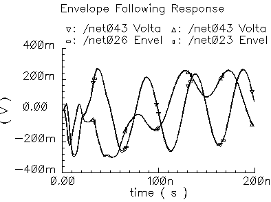
demod_ip3
(baseband = IQ_demod_BB, passband = IQ_demodulator)
Figure 1-79 Baseband and Passband IQ Demodulator Models
The IQ_demodulator converts RF (or IF) to baseband. Figure 1-80 shows exactly what the passband demodulator model does. The parameters are like those in the modulator blocks except saturation is specified by input referred IP3 instead of by 1 dB compression point. IP3 was chosen over the 1 dB compression point for specifying saturation because the demodulator usually lies in the receive path and receiver blocks are usually specified with IP3.
Figure 1-80 IQ Demodulator Calculations
The circuit called demod_ip3 in the testbenches category of the rfLib shows how the gain and IP3 parameters are defined. Figure 1-81 shows the schematic. Both the input and the output resistances are matched.
Figure 1-81 The demod_IP3 Schematic
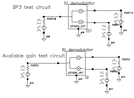
-
Recall the
demod_IP3circuit and set up a swept PSS analysis. Let the Beat Frequency be Auto Calculated. Keep 2 harmonics. Sweep the power parameter from -100 to 0 in 10 linear steps. - Set up a single point PAC analysis at 921 MHz and keep the -25 and -21 sidebands.
-
After running the analysis, from the PAC output window plot the input-referred IP3 curves with 81 MHz as the 3rd order sideband and 79 MHz as the 1st order sideband. The procedure is similar to the mixer IP3 example covered in “(IQ Modulator Models)”. Use Variable Sweep for the Circuit Input Power and -100 for the Extrapolation point. Make sure to plot Input Referred IP3. Click the
I-outputport in the top circuit. You should see -10 dBm as the IP3, just as specified. Figure 1-82 shows the IP3 plot. Note that 1st order line indicates the gain is 3dB below the specified gain of 0 dB. That is because not all of the power lies at 1000 MHz-921 MHz = 79 MHz; Some of the power lies at 1000 MHz + 921 MHz = 1921 MHz. Use the bottom test circuit to measure available power gain. The bottom circuit drives the demodulator at the same frequency as the demodulator’s internal local oscillator, which runs at 1 GHz. Now the output power is not split, it lies in the zero harmonic of theI-output.
Figure 1-82 Demodulator IP3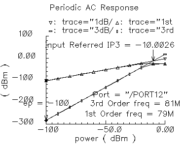
-
Plot the 1dB compression point at the port loading the
I-outputof the bottom circuit. Use the zeroth harmonic. The ratio of output to input power should be unity in the linear region. Figure 1-83 shows the compression point plot. The measured 1dB compression point is of no use in this test. We want the gain. At low power levels where the gain is constant, the gain is as specified. -
Remember, in this test circuit the load resistance and output resistance are equal so that the output power is maximal. Also, the input resistance equals the source resistance so that the horizontal axis truly equals input power.
Figure 1-83 Demodulator Available Power Gain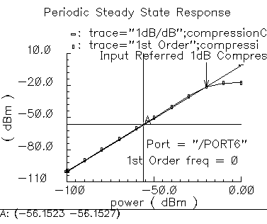
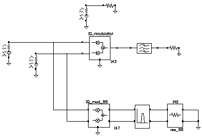
Phase errors behave like their counterparts in the modulator models except for a change of sign. Quadrature error behaves exactly as it does in the modulator models. Figure 1-84 shows a test circuit for illustrating the relationships between phase error and quadrature error in the modulators and demodulators. The test circuit is called mod_demod_test and is listed in the testbenches category. The test circuit also shows that the passband and baseband models give comparable results, as they should, as long as the passband carrier is not severely clipped. The baseband input trajectory is a complex 1 MHz tone, which produces a circular input trajectory. The demodulator outputs are not matched and are not symmetric with respect to I and Q paths. The modulators and demodulators are not perfectly linear and the non-linearities are asymmetric with respect to I and Q. The modulators and demodulators are driven by the same phase error and the quadrature error parameters are a common variable set to 0.785 radians.
Figure 1-84 mod_demod_test Circuit
To use the mod_demod_test circuit:
-
Recall the circuit and set up a 5 us Envelope analysis with
carrieras the Clock Name. -
After the analysis completes, plot the
IQ_mod_BBoutputs and make theI_outsignal the x-axis. -
Open a subwindow and in it, plot the harmonic time waveforms of the
IQ_modulatoroutput. Use the first harmonic and plot the real and imaginary waveforms. Make the real waveform the x-axis. - Open a third subwindow and stretch the Waveform Display window so that the third subwindow appears below the first window.
-
Plot the time waveforms at the
IQ_demod_BBoutputs and make theI_outwaveform the x-axis. -
Open a fourth subwindow and plot the harmonic time results at the
IQ_demodulatoroutputs but this time use the zeroth harmonic and only plot the real parts. Make theI_outwaveform the x-axis. Figure 1-85 shows what you should now see.
The leftmost pictures are from the baseband models and the rightmost are from the passband models. Passband and baseband models agree quite well. The top pictures are the voltages at nodes that lie between the modulator and demodulator. Quadrature error squashes the baseband trajectory at that node. The trajectory precesses because phase error ramps up linearly with time just like in the last test. The non-linearities produce the sharp corners. The bottom trajectories do not precess because the same phase error rotates the demodulator output in the reverse direction; driven by the same phase error ramp, the demodulator undoes the precession introduced in the modulator. The demodulator outputs are nearly in phase because the quadrature errors of pi/4 in the modulators and demodulators add to give a total quadrature error of π/2, which in this case puts the baseband I and Q outputs nearly in phase with each other.
dwn_cnvt_test
(RF-to-IF and IF-to-RF Mixers)
(passband = MIXER_PB, baseband = dwn_cnvrt and up_cnvrt)
Figure 1-86 Baseband and Passband Mixer Models
MIXER_PB is a passband model that converts RF to IF and IF to RF. dwn_cnvrt model is a baseband equivalent model of a mixer used to convert from RF to IF. up_cnvrt model is a baseband equivalent model of a mixer used to convert from IF to RF. There are some minor differences in the baseband models that depend on whether conversion is up or down. Figure 1-87 and Figure 1-88 show what the models do.
Figure 1-87 Calculations for up_cnvrt Mixer
Figure 1-88 Calculations for dwn_cnvrt Mixer
The noise figure and IP3 parameters are defined in “(IP3 Parameter)”. Unlike the IQ_demodulator, the IP3 test circuit can be used to define the available power gain because the gain is defined from the input frequency to just one sideband.
Typically the mixer would be used to create an IF stage. In that case, it is difficult to obtain a simple (i.e. filterless) envelope analysis that overlays waveforms to show how well baseband and passband models agree. The test circuit shown in Figure 1-89, which is listed as dwn_cnvt_test in the testbenches category of the rfLib, shows the relationship between baseband and passband models. The top branch of the circuit consists of passband models. The bottom branch consists of baseband models.
Figure 1-89 dwn_cnvrt_test Circuit
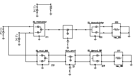
-
Recall the circuit and set up a 200 ns envelope analysis with
fclckas the Clock Name. Keep 1 harmonics1. -
After the analysis completes, plot the “time” waveform at the
I_outpin of theIQ_demod_BBmodel. Append to the plot, the harmonic-time, real part of the zero harmonic of theI_outpin on theIQ_demodulatormodel. -
Open a subwindow and do the same for the
Qoutputs. You should now see a picture like the one in Figure 1-90.
Figure 1-90 Output from an Envelope analysis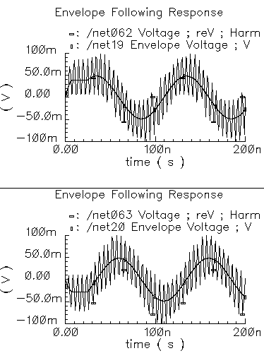
To understand these results, trace the input signal through the passband branch. A complex baseband 10 MHz tone drives both branches. The modulator’s local oscillator is 1 GHz so that the IQ_modulator output is at 1.01 GHz. There is no 990 MHz sideband because the input baseband trajectory is a circle (= sin + jcos), which represents a complex tone. The mixer local oscillator is 900 MHz, which when mixed with 1.01 GHz, produces 110 MHz and 1.91 GHz. The IQ_demodulator local oscillator is 100 MHz, which produces 10 MHz, 210 MHz, 2.01 GHz, and 1.81 GHz. The 10 MHz and 210 MHz terms dominate the zero harmonic at the demodulator outputs. The higher frequencies average out to nearly zero. The baseband output is the 10 MHz term and that is what the baseband branch generates, as shown in Figure 1-90. A Transient analysis actually runs about 13 times faster than envelope on this circuit. Figure 1-115 compares the same outputs using a Transient analysis.The Transient analysis shows that the zero harmonic of the envelope analysis averaged out all frequencies above the envelope clock frequency (1 GHz).
mixer_ip3
IP3 is measured with a two-tone test. One tone is the fundamental PSS frequency while the other is the frequency in a single point PAC analysis. IP3 is defined as the input power level in dBm where the extrapolated power in one of the third order intermodulation terms equals the extrapolated power in the fundamental term. As with the 1dB compression point measurement, input and output terminals must be matched to the source and load respectively.
The IP3 specification is demonstrated step by step on the mixer model because the mixer IP3 measurement can be confusing. Figure 1-91 shows the test circuit. The circuit is listed as mixer_ip3 in the testbenches category of the rfLib. For guidance on using the test circuit, see “Measuring IP3 for a Mixer”.
Figure 1-91 The mixer_ip3 Test Circuit
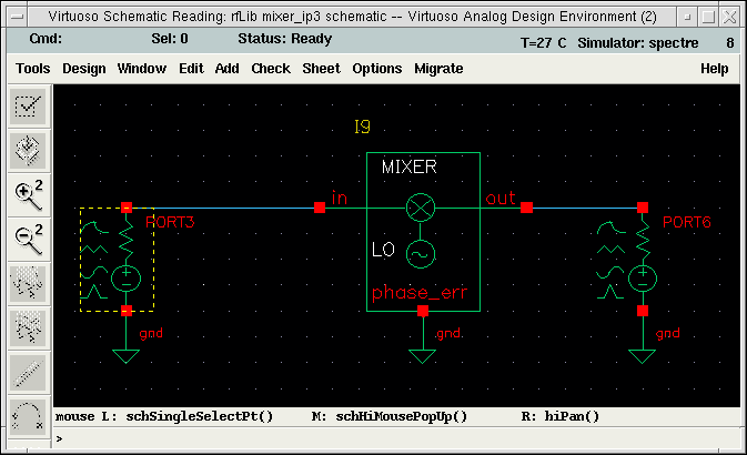
Measuring IP3 for a Mixer
For information about the test circuit used in this example, see “(IP3 Parameter)”.
- Open the schematic for the circuit and bring up ADE.
-
In the Virtuoso Analog Design Environment window, choose Analyses – Choose.
The Choosing Analyses form appears. -
Set up a PSS analysis.
-
Select pss.
The title Periodic Steady State Analysis appears along with the fields required for specifying a PSS analysis.
A 920 MHz tone already appears in the form. -
Add a Fundamental Tone called
eee(the name is arbitrary) with a Value of 1 GHz. - Select Beat Frequency.
-
Click Auto Calculate.
The result is40MHz. - For the Number of harmonics, type 2.
- Select Sweep.
-
For the Variable Name, use the
powervariable. - Set Frequency Variable to no.
- In the Sweep Range pane, select Start_Stop.
- In the Start field, type -60.
- In the Stop field, type 0.
- Select Linear.
- Select Number of Steps.
- In the Number of Steps field, type 10.
-
Select pss.
-
Set up a PAC analysis.
-
Select pac.
The title Periodic AC Analysis appears along with the fields required for specifying a PAC analysis. - Set Sweeptype to absolute.
- Select Single-Point.
- In the Freq field, type 921 M.
- In the sidebands pane, select Array of indices.
- In the Additional indices field, type -21 and -25.
After these steps, the Choosing Analyses form looks like this.
Figure 1-92 Choosing Analyses PAC SetupWhy select the -21 and -25 sidebands? Recall from the assumptions, the non-linearity occurs before the frequency translation. The input tones to the non-linearity are the large 920 MHz tone and the small signal 921 MHz tone. In an IP3 measurement only one tone must be large, the other can be small. PAC analysis performs small signal perturbations on the PSS solution. One perturbation term exiting the non-linearity appears at 921 MHz, right where it started. One of the third order intermodulation perturbation terms exiting the non-linearity appears at 2*920-921 = 919 MHz. The ideal mixer, driven by a pure 1 GHz local oscillator, translates the 921 MHz tone to 921-1000=-79 MHz while translating the 919 MHz tone to 1000-919=81 MHz. A single point 921 MHz PAC analysis produces tones displaced from harmonics of the fundamental by 921 MHz. The PAC sidebands specify which harmonics to use. You save the 79 MHz tone by saving the -25th sideband because the fundamental frequency is 40 MHz and 921 - 40*25 = -79 MHz. You save the 81 MHz tone by saving the -21 sideband because 921-40*21 = 81 MHz. Figure 1-92 shows the PAC setup.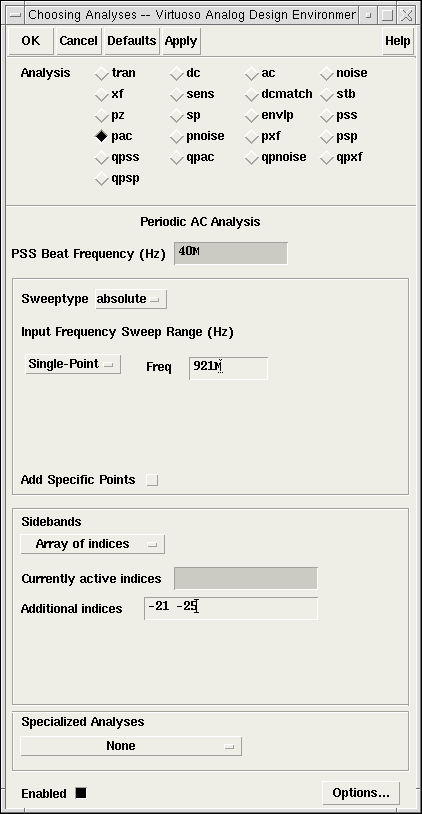
-
Select pac.
- Run the analysis.
-
Plot the PAC results. To do this, set up the Direct Plot form like this.
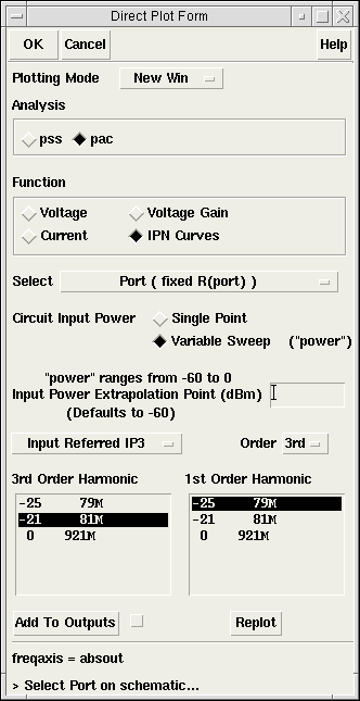
-
In the Composer window, click the output Port. The results appear as shown in Figure 1-93.
Figure 1-93 IP3 Results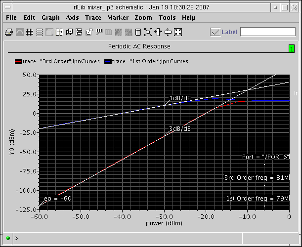
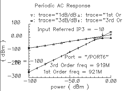
The measured IP3 is, -10 dBm, as specified. The measured IP3 is as specified only if the input port resistance matches the input resistance of the device-under-test. Other input resistances produce a measured IP3 different than the one specified.
Measuring IP3 for an LNA
You can measure IP3 of an LNA by replacing the mixer with an LNA and ensuring the input terminal remains matched. In this example, remove the 1 GHz Fundamental Tone from the PSS analysis. The Beat Frequency should now be 920 MHz. In the PAC set up, change the additional indices from -21 and -25 to -1 and -2.
After the analysis completes, set up the PSS Results form as shown in Figure 1-94. As in “Measuring IP3 for a Mixer”, the input referred IP3 is 10 dBm, as specified. Figure 1-95 shows the LNA IP3 results.
Figure 1-94 Direct Plot Form for the LNA
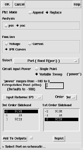
Figure 1-95 Results for the LNA
mod_1dbcp
(Available Power Gain and 1dB Compression Point)
Available power gain of the IQ-modulator is best explained with an example. Recall the circuit called mod_1dbcp listed in the testbenches category of the rfLib. The schematic contains two disjoint circuits. One shows how not to measure gain and compression point, the other shows the proper measurement.
-
Set up a PSS analysis. Both test circuits run in the same simulation. The beat frequency is 100 MHz. Save the first and 11th harmonics. In the options, set
maxstepto 50 ps. Sweep the variablepowerlinearly in 50 steps from -40 to 15. - After the analysis completes, plot the output referred 1dB compression point of the top circuit using -40 dBm as the Extrapolation point. First select the 11th harmonic (1.1 GHz) and click the output port in the top test circuit, the bad test circuit. Note that the linear gain is 3 dB lower than specified, as is the output referred 1dB compression point. The gain was specified as zero dB and the 1dB compression point was 10 dBm. The error arises from the fact that the input signal power splits between upper (1.1 GHz) and lower (900 MHz) sidebands but the ADE measurement only looks at one output sideband. The bottom test circuit resolves the ambiguity by defining the gain of the IQ-modulator as the gain from the baseband input to an ideally-demodulated baseband output. The bottom test circuit follows the IQ-modulator with an ideal IQ-demodulator. The gain of the demodulator is zero dB and the 1dB compression point is high enough to render the demodulator distortionless.
-
Repeat the steps for plotting the 1dB compression point but this time chose the first harmonic and select the output port that loads the bottom circuit. Select the first (100 MHz) harmonic and plot the 1dB compression point again. Now you should see a 1dB compression point plot that reflects the specified parameters of the IQ-modulator. The gain is now also correct, which can be computed from the ratio of the output to input power well below the compression point. Figure 1-97 shows such a plot.
Figure 1-96 1db Compression Point Test CircuitFigure 1-97 1db Compression Point Plot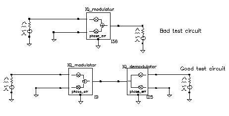
mod_demod_test
See “demod_ip3”.
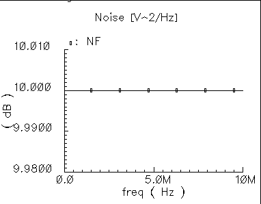
noise_figure
Noise figure is calculated as the input signal-to-noise ratio divided by the output signal-to-noise ratio. The test circuit for defining the noise figure parameter is shown in Figure 1-98. The circuit is listed as noise_figure in the testbenches category of the rfLib. It is similar to the one_db_cp test circuit.
Figure 1-98 The noise_figure Circuit
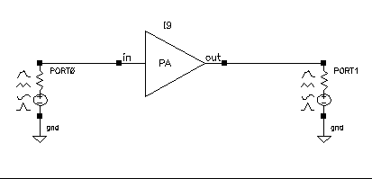
The specified noise figure is 10 dB. A Spectre RF Noise analysis produces the noise figure shown in Figure 1-99. To measure the specified noise figure, the driving port resistance must match the amplifier’s input resistance. The port at the output does not have to match the amplifier’s output resistance but the port impedance should be resistive. The input probe is the leftmost port, the output port is the rightmost port. Because the model is static, you can compute noise figure over any frequency interval.
Figure 1-99 Noise Figure Results
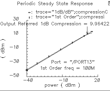
one_db_cp
(Output 1dB Compression Point Parameter)
The 1 dB compression point specifies a saturation non-linearity. It is the output power in dBm where the output power falls 1 dB below the power extrapolated linearly from the amplifier’s linear region of operation.
The test circuit in Figure 1-100 is listed as one_db_cp in the testbenches category in rfLib.
Figure 1-100 The one_db_cp Circuit
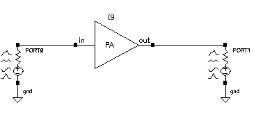
In the one_db_cp test circuit, power is the dBm of power delivered by the leftmost port. The available power gain is 0 dB. The 1dB compression point is 10 dBm. The input and output resistances are 50 Ohms and so are the port resistances.
To measure the 1dB compression point, perform a swept PSS analysis. Sweep power from -40 dBm to 15 dBm in 50 linear steps. The output referred 1dB compression point is computed for the 1st harmonic with an Extrapolation Point [dBm] of -40. Click the rightmost port device to display the output as illustrated in Figure 1-101.
Figure 1-101 Resulting 1dB Compression Point
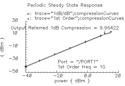
The specified output referred compression point is 10 dBm. The measured value is 9.964 dBm, which is fairly close to the specified value. The measured 1db compression point is as specified only when the driving source resistance matches the amplifier input resistance and the load port resistance matches the amplifier’s output resistance. In all compression point and IPN calculations, input power is computed from the maximum power the input Port can deliver, not from an actual power measurement. If you mismatch either terminal you do not measure the specified compression point.
PB_BB_filter_comparison
See “BB_ind_cap_test”.
PB_ind_cap_test
See “BB_ind_cap_test”.
quad_and_phase_error_demo
(Quadrature Error and Phase Error)
Quadrature error describes how far away from 90 degrees the two local oscillators are from each other. Ideally, they are exactly 90 degrees, or π/2 radians, apart in phase. In practice, parasitics and asymmetric delays can drive the phase shift away from π/2. Figure 1-102 show a baseband test circuit and its passband equivalent. The schematic is listed in the rfLib testbenches category under the name quad_and_phase_error_demo. Both circuits are driven from a common set of baseband sources. The test circuit serves two purposes, it shows the correspondence between baseband and passband models and it demonstrates how quadrature error and phase error affect the baseband trajectory. The baseband input signal is a complex tone, which makes a circular input baseband trajectory. If there were no quadrature error, the baseband representation of the modulator output would also be a circle. With quadrature error, the output trajectory is an ellipse. If the phase_err pins are driven by a ramp, the ellipse precesses. The ramp represents a small but fixed difference between carrier and local oscillator frequencies.
Figure 1-102 quad_and_phase_error_demo Circuit
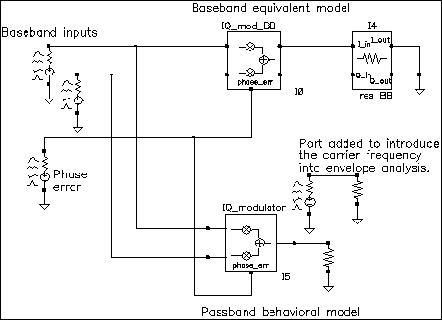
-
Set up an ENVLP analysis with
carrieras the Clock Name. Simulate 10 us of action and save the first harmonic. -
When the analysis completes, open the Envelope Following Direct Plot form and set the sweep to time. Plot the two outputs of the
IQ_mod_BBblock. -
Change the x-axis to be the
I-output. You should see the left trajectory in Figure 1-103. - Add a subwindow for the passband equivalent result.
-
In the Direct Plot form, change the sweep to harmonic time and plot the real and imaginary parts of the first harmonic of the
IQ_modulatoroutput voltage. -
Change the x-axis to be the real part of the first harmonic. You should now have two plots that match those in Figure 1-103.
Figure 1-103 Output Trajectories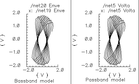
shifter_combiner_test
The phase shifter-combiner has two inputs and one output. The inputs are phase shifted by +/- 45 degrees then added together to form the output. All terminals are buffered and have the specified terminal resistances. The phase shifts are accomplished with Verilog-A code that does the same thing as the circuit shown in Figure 1-104. The gains of the left-most voltage-controlled-voltage sources are user-defined. The input resistance, output resistance, intended operating frequency, and internal resistance are also user-defined. The internal resistance and operating frequency are used to calculate the capacitance necessary to provide 45 degrees of phase shifts at the operating frequency. The baseband view requires that the carrier frequency be specified.
Figure 1-104 Phase Shift Circuit
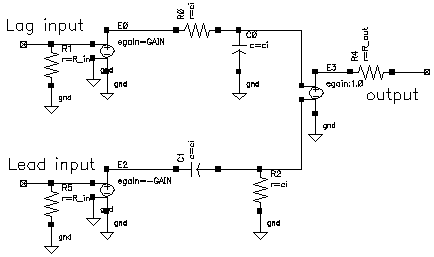
The shifter-combiner can be used to eliminate one phase of the carrier. The test circuit in Figure 1-105 shows a simple test to demonstrate the idea. The circuit is in the rfLib under the testbenches category and listed as shifter_combiner_test. The top circuit is a passband model and the bottom circuit is the baseband equivalent. Baseband input signals are mixed up to 1GHz then passed into the shifter-combiner. The baseband signal contains 10MHz and 20Mhz components. The modulators and shifter-combiner are arranged to produce only a 20MHz signal riding on the carrier.
Figure 1-105 shifter_combiner_test Circuit
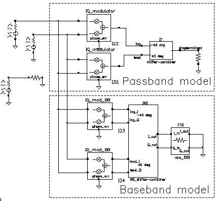
- Bring up the test circuit and an Analog Environment window.
-
Set up a 100ns envelope analysis on the circuit with the Clock Name set to
carrierand the modulationbw option set to 40MHz. Set the Harmonic number to 1. - Run the analysis.
- Plot the harmonic time, 1 Harmonic, and the real and imaginary parts of the passband shifter combiner output.
-
Append to the plot, the
timewaveforms at theI_outandQ_outpins of theBB_shifter _combinermodel. Figure 1-106 shows what you should see in the Waveform Display window. All waveforms are the same and they contain only the 20Mhz baseband signal. The 10Mhz baseband input signal does not propagate to the output.
Figure 1-106 shifter_combiner_test results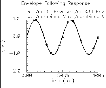
One application of the shifter-combiner is an image rejection receiver. Figure 1-107 shows a very simple example of an image rejection receiver. Figure 1-108 shows the baseband equivalent model of the receiver. Both examples are in the rfExamples directory and are listed as image_reject_rcvr_PB and image_reject_rcvr_BB. The local oscillator runs at 1GHz and the RF carrier is 1.1GHz, which places the image at 900Mhz. This example shows one of the limitations of the baseband equivalent models.
Figure 1-107 A Simple Image Rejection Receiver
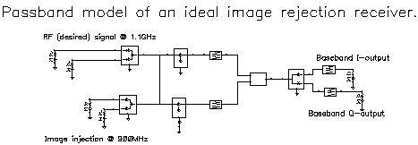
Figure 1-108 Baseband Equivalent Model of the Image Rejection Receiver
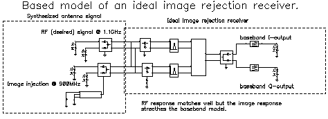
- Bring up the passband test circuit and an Analog Environment tool.
- Set up a PSS analysis. You need to add the 1.1GHz, 1GHz, and 900Mhz fundamental tones. Give them arbitrary but distinct names. AutoCalculate the Beat Frequency, which should be 2MHz. You need not save more than the 1st harmonic. Set the PSS maxstep option to 20ps so that it accurately simulates the oscillators hidden inside the Verilog-A modules.
- Run the analysis.
- Plot the voltages across Ports 5 and 6. Set the x-axis to be the voltage across Port 6. This is a Lissajous plot of the desired baseband signal, the one riding on the 1.1GHz carrier.
- Add a subwindow.
- Plot the voltages across Ports 8 and 7. Set the x-axis to be the voltage across Port 8. This is a Lissajous plot of the undesired baseband signal, the signal riding on the image of the carrier at 900MHz.
- Add another subwindow.
- Plot the I and Q- baseband outputs. Set the x-axis to be the I-output. The Lissajous plot is a tilted version of the desired baseband signal, indicating that most of the image was successfully rejected.
- Bring up the baseband equivalent receiver model and another Analog Environment tool.
- Run a 10us Transient analysis with 9.5us as the output start in the analysis options and maxstep set to 250ps. The phase_err pin on the image signal generator is being driven to spin the output at 200MHz, the frequency difference between the desired frequency and image frequency.
- Add another subwindow to the Waveform Display tool showing the passband results and make sure it is active.
-
Plot the I and Q baseband outputs from the baseband equivalent receiver model. Set the x-axis to be the I-output. You might need to adjust the scales on the last two plots to make them the same. Aside from the labels, the Waveform Display tool should look like Figure 1-109.
Figure 1-109 Lissajous Plots for Baseband Signals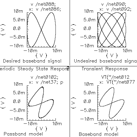
The baseband equivalent receiver model indeed rejects the image but the rejection is over-estimated. If you look closely, the baseband output of the passband model contains more ripple from the image. The over-attenuated ripple in the baseband model is explained as follows.
Recall the rotating reference frame analogy for baseband modeling. With respect to the rotating 1.1GHz reference frame, the image signals rotate counter-clockwise at twice the IF, 200MHz in this case. The lower left block in the baseband receiver model spins the modulator output at -200Mhz by ramping the phase error pin. The -200MHz signal propagates through the IF bandpass filters, as it should, because the response of the baseband model of the filter peaks at DC and at minus 200MHz. The trouble occurs in the final downconversion to baseband. In the baseband model, the final low pass filters severely attenuate the -200Mhz image signal. However, in the passband model, image power at minus 100MHz contributes to the baseband signal through the low pass filters with less attenuation.
This example highlights one of the limitations of baseband equivalent models: at any point in the system, the signal should not have a bandwidth larger than any carrier (RF or IF) of the system. For this example, the baseband model is only valid for input RF signals between 1GHz and 1.2GHz.
The limitation is somewhat moot because the idea behind a baseband equivalent model is to suppress all carriers. To simulate the image response with the baseband model we had to include a 200MHz source! We would have been better off simply not suppressing the 100MHz IF carrier, i.e. using baseband models for the RF stages but passband models for the IF stages.
In summary, an all-baseband equivalent model of an image rejection receiver is only good for simulating the response to the desired RF signal, not the image response.
shifter_splitter_test
The phase shifter-splitter has one input and two outputs. The outputs are phase shifted versions of the input at the specified frequency. The phase difference between the two outputs is 90 degrees. The phase shifts are accomplished with Verilog-A code that does the same thing as the circuit shown in Figure 1-110. The right-most voltage-controlled-voltage-sources (vcvs) are unity gain buffers. The left-most vcvs is also a buffer but the gain is a user-defined parameter. The input resistance, output resistance, intended operating frequency, and internal resistance are also user-defined. The internal resistance and operating frequency are used to calculate the capacitance necessary to provide +-45 degrees of phase shifts at the operating frequency. The baseband view requires the carrier frequency.
Figure 1-110 Phase Shift Circuit
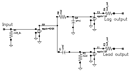
The test circuit in Figure 1-111 is for comparing the baseband responses of the passband and baseband equivalent models of the shifter-splitter. The circuit can be found in rfLib under the testbenches category. It is listed as shifter_splitter_test.
Figure 1-111 shifter_splitter_test Circuit
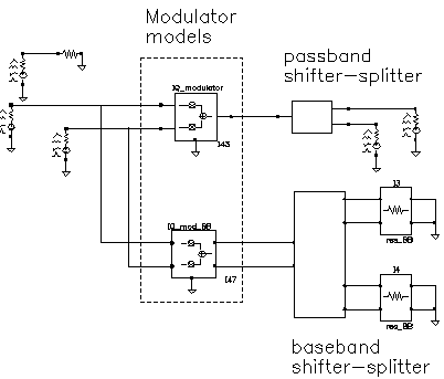
The following steps produce a set of Lissajous plots that show what the shifter-splitter does. You observe phase shift in the carrier by observing the tilt of the output Lissajous figures generated by the equivalent baseband signals.
- Bring up the test circuit in Figure 1-111 and an Analog Environment window.
-
Set up a 200ns Envelope analysis with
carrieras the Clock Name. Set the Number of harmonics to 1. Set the Envelope analysis option called modulationBW equal to 100MHz. - Run the analysis.
-
Plot the
timewaveforms of the two input baseband signals. Change the x-axis to be the I-signal. You should see the Lissajous plot in Figure 1-112.
Figure 1-112 Lissajous Plot for Baseband Input Signals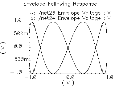
- Reset the Waveform Display window and plot the harmonic time, 1 harmonic, real and imaginary parts of the voltage across Port2. Set the x-axis to be the real part. Note that the Lissajous plot is tilted -45 degrees from the one in Figure 1-112.
- Add a subwindow.
- Repeat step 5 for the voltage across Port1. Notice that the Lissajous plot is tilted +45 degrees with respect to the Lissajous plot in Figure 1-112.
- Add another subwindow.
-
Plot the
timewaveforms at thelag_Iandlag_Qoutputs of theBB_shifter_splittermodel. Set the x-axis to be the lag_I waveform. The Lissajous plot should match the one produced in step 5. - Add another subwindow.
-
Repeat step 9 for the
leadoutputs of theBB_shifter_splittermodel. The Lissajous plot should match the one produced in step 7. Aside from the labels, your Waveform Display tool should look like Figure 1-113. The time-results of the baseband model faithfully duplicate the passband results but without simulating the carrier. The baseband model can be run with Spectre RF transient analysis.
Figure 1-113 Comparison of Lag and Lead times for Passband and Baseband Models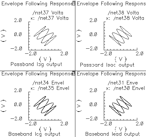
up_cnvt_test
There is a test circuit for the up_cnvrt model similar to the test circuit containing the dwn_cnvrt model. The up_cnvrt model is called up_cnvt_test and is shown in Figure 1-114. It is also in the testbenches category of rfLib. The steps parallel those for the dwn_cnvrt model.
Figure 1-114 up_cnvt_test Circuit
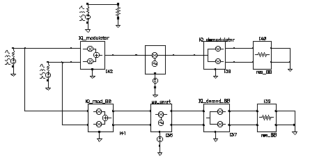
Figure 1-115 Results from a Transient Analysis
view_switching
This example illustrates how to switch between the single-ended baseband view and the differential passband view.
WCDMA_components Category
The components in the WCDMA_components category are:
- wcdma_dl_com_chanl
- wcdma_ocns
- wcdma_power_adjust
- wcdma_qpsk
- wcdma_sch_multiplexer
- wcdma_scrambling
- wcdma_scr_generator
- wcdma_spreading
wcdma_dl_com_chanl
Figure 1-116 wcdma_dl_com_chanl symbol
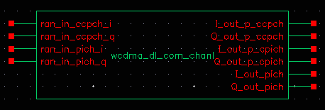
This module, with four inputs and six outputs, generates the pCPICH (primary common pilot), PICH (paging indicator channel) and pCCPCH (primary common control physical channel). For PICH and pCCPCH, either external or internal random signals can be selected according to the value of the enable_input parameter. The parameters of the module are:
| Name | Meaning | Type | Default Value | Range |
|
|
||||
|
|
||||
|
|
wcdma_ocns
Figure 1-117 wcdma_ocns symbol
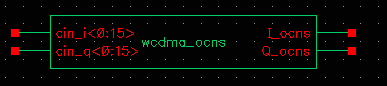
This module produces the combination of 16 dedicated data channels. The parameters of the module are:
| Name | Meaning | Type | Default Value | Range |
|
|
||||
wcdma_power_adjust
Figure 1-118 wcdma_power_adjust symbol
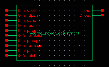
This module applies the weight to different channels. The parameters of the module are:
| Name | Meaning | Type | Default Value | Range |
|
|
||||
|
|
||||
|
|
||||
|
|
||||
|
|
wcdma_qpsk
Figure 1-119 wcdma_qpsk symbol
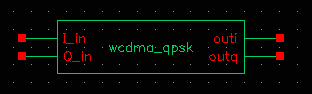
This block has two inputs, I_in and Q_in, and two outputs, outi and outq. The inputs receive random input from outside the module. The outputs produce QPSK signals in baseband.
- This module includes the interleaving and encoding of data.
-
You can use either random input from the outside or internal random bits. If
enable_inputis on, external data is used, otherwise internal random bits are used.
The instance parameters for the wcdma_qpsk block are:
| Name | Meaning | Type | Default Value | Range |
|
|
||||
|
|
||||
|
|
||||
|
|
wcdma_sch_multiplexer
Figure 1-120 wcdma_sch_multiplexer symbol
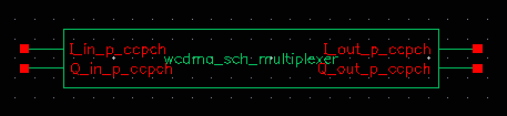
This module produces the synchronization channel and performs SCH multiplexing. The parameters of the module are:
| Name | Meaning | Type | Default Value | Range |
|
|
||||
|
|
||||
wcdma_scrambling
Figure 1-121 wcdma_scrambling symbol
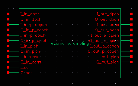
This module scrambles the spread code. The parameters of the wcdma_scrambling module are:
| Name | Meaning | Type | Default Value | Range |
|
|
wcdma_scr_generator
Figure 1-122 wcdma_scr_generator symbol
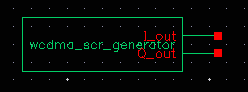
This module up-samples and filters the input. The parameters of the module are:
| Name | Meaning | Type | Default Value | Range |
|
|
|
|||
|
|
|
|||
|
|
||||
|
|
|
wcdma_spreading
Figure 1-123 wcdma_spreading symbol
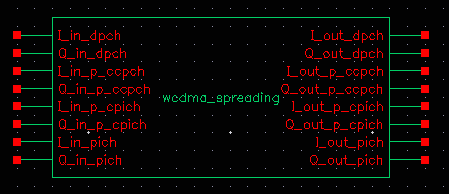
This module spreads the data over the OVSF codes. The parameters of the wcdma_spreading module are:
| Name | Meaning | Type | Default Value | Range |
|
|
||||
|
|
||||
|
|
||||
|
|
||||
|
|
||||
|
|
||||
Wireless Components Category
Wireless components automate the measurements associated with modulated signals. The supported standards are Zigbee, 802.11a, 802.11n, 802.11ac, 802.11ad, 802.11af, 802.11ah, 802.11p, 802.11ax, Bluetooth (BR, EDR, LE, and HS modes), smart meter, dmr, LTE, NR, and Msource. To use wireless, add a wireless source to your circuit, and add wireless probes at each point in the circuit where you want a measurement. When you set up the envelope analysis, put envelope into wireless mode, and specify the number of harmonics and whether you want standard envelope or level1 fast envelope. Run the simulation. In the Direct Plot Form, all the common measurements are available directly. This is much easier than in the past.
LTE
SYMBOL
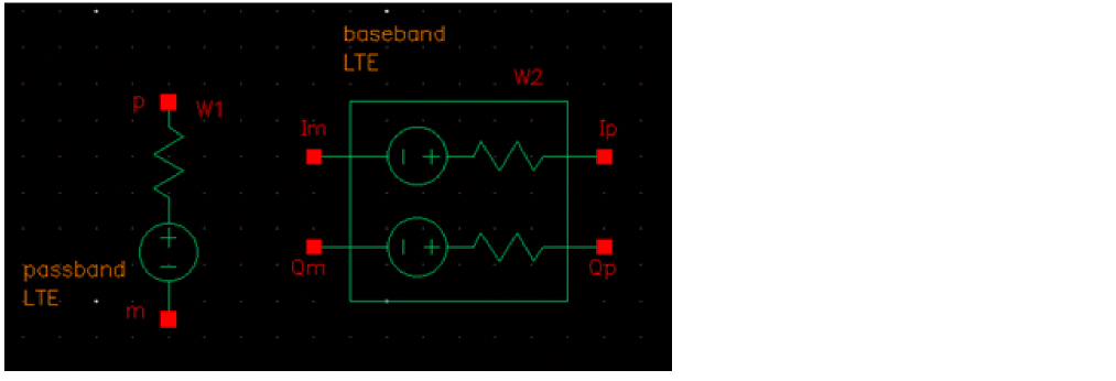
LTE Modulation Source
Command-line Help
spectre -h wsource
CDF Parameters
Parameter Description
- Signal type: Sets the passband or baseband operating mode.
- Source type: Specifies the type of wsource in the design.
- Carrier harmonic: Specifies the carrier harmonic for the LTE source.
-
LO source type: Specifies the type of local oscillator. Possible values are
I&Qandsingle. This parameter is available only for the passband operating mode. - LO/I source name: Specifies the name of the local oscillator I path. This parameter is available only for the passband operating mode.
- LO/Q source name: Specifies the name of the local oscillator Q path. This parameter is available only for the passband operating mode.
- LO source name: Specifies the name of the local oscillator. This parameter is available only for the passband operating mode.
- Average Power: source available average power in dBm
- Resistance: source Thevenin resistance
- Number of SF (FDD)/HF (TDD): The number of subframes to simulate.
- Oversample ratio: Controls the sampling frequency. If ACPR Type is set to UTRA and Channel bandwidth is specified as 200k, the value should be greater than or equal to 3. The sampling frequency is given by oversample*32.72MHz.
- SNR: Signal-to-noise power ratio.
- Operating band: Operating band given by TS36.101 Table 5.5-1, in the set {[1:14], [17:28], [30:31], [33-48], 65-66], [68], [70]}. Band [33-48] is TDD mode while the others are FDD mode.
-
FDD or TDD Mode: Selects the FDD or TDD Mode. In the default TDD mode, two out of five subframes are populated. In FDD mode, all subframes are populated. Possible values are
FDDandTDD. This option is displayed only when the operating band is in the range [33:48]. - Direction: Direction of uplink or downlink. Possible values are UL and DL.
- Channel number: E-UTRA Absolute Radio Frequency Channel Number given by TS36.101 Table 5.7.3-1, in the set {(18000:27809), (36000:55239), (131072:133221)}.
- Channel bandwidth: E-UTRA channel bandwidth given by TS36.101 Table 5.6.1-1, in the set {200K, 1.4M, 3M, 5M, 10M, 15M, 20M}.
- Modulation type: Specifies the modulation type. For LTE, it is QPSK, QAM16, and QAM64. For NB1 uplink, it is QPSK and BPSK. NB1 downlink always uses QPSK. Possible values are QPSK, QAM16, QAM64, and BPSK.
- Channel offset: Specifies the offset from the NB1 channel number center frequency. For UL, it is in the set {-10, -9, -8, -7, -6, -5, -4, -3, -2, -1, 0, 1, 2, 3, 4, 5, 6, 7, 8, 9}. For DL, it is in the set {-10, -9, -8, -7, -6, -5, -4, -3, -2, -1, -0.5, 0, 1, 2, 3, 4, 5, 6, 7, 8, 9}.
- Subcarrier spacing: Specifies the subcarrier spacing for NB1 uplink in the set {15K, 3.75K}.
- Number of tone: Specifies the number of tones for NB1 uplink category. For 15K subcarrier spacing, it is in the set {1, 3, 6, 12}. For 3.75K subcarrier spacing, it is 1.
- Tone start index: Specifies the tone start index for the NB1 uplink category.
-
Resource Block Allocation: Choices are
FullandPartial. WhenFullis selected, all the resource blocks in the channel are fully populated. WhenPartialis selected, the number of resource blocks and their location within the channel must be set. -
Resource Block Number: This sets the number of resource blocks that are occupied in the channel. The number should be 2^m * 3^n * 5^p where m, n, p >= 0. Each resource block occupies 180KHz bandwidth. The maximum number depends on the channel bandwidth. The maximum is shown in the table below.
- Starting Index of RB: This sets the starting point in the channel for the resource blocks. Zero means start at the lower boundary of the channel. The starting index + number of resource blocks must be equal to or less than the maximum number shown in the table above.
- Number of carriers in CA: This sets the number of carriers intra band channel aggregation. The default is 1. Values from 1 through 5 are selectable. Note that when set from 2 through 5, the EVM plot shows considerably larger values than are real. This option is available only when Channel bandwidth is set to 3M, 5M, 10M, 15M, or 20M.
- ACPR Type or CIM: This is selectable between EUTRA, which is the default, UTRA, and CIM. These settings are defined in 36101 section 6.6.2.3.1 for EUTRA and 6.6.2.3.2 for UTRA.
-
Downlink signal type: Specifies the downlink signal type. When set to PDSCH&CRS, both PDSCH and CRS are transmitted. When set to PDSCH, only PDSCH is transmitted. When set to CRS, only CRS is transmitted. Possible values are: PDSCH&CRS, PDSCH, and CRS.
Example
W0 ( net2 net1 ) wsource standard="LTE" r=50 dbm=10 LTE_Band=1 LTE_ChannelNumber=18050 LTE_Bandwidth=10M LTE_Modulation=QAM16 framenumber=1 oversample=4
NR
SYMBOL
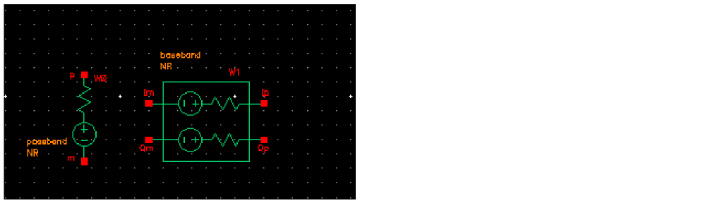
NR Modulation Source
Command-line Help
spectre -h wsource
CDF Parameters
Parameter Description
- Signal type: sets the passband or baseband operating mode.
- Signal type: Specifies the type of wsource in the design.
- Carrier harmonic: Specifies the carrier harmonic for the NR source.
-
LO source type: Specifies the type of local oscillator. Possible values are
I&Qandsingle. This parameter is available only for the passband operating mode. - LO/I source name: Specifies the name of the local oscillator I path. This parameter is available only for the passband operating mode.
- LO/Q source name: Specifies the name of the local oscillator Q path. This parameter is available only for the passband operating mode.
- LO source name: Specifies the name of the local oscillator. This parameter is available only for the passband operating mode.
- Average Power: source available average power in dBm.
- Resistance: source Thevenin resistance.
- Num of half subframes: The number of subframes to simulate.
- Oversample ratio: Controls the sampling frequency. The sampling frequency is given by oversample*Subcarrier spacing*4096.
- SNR: Signal-to-noise power ratio.
-
Operating band: Operating band given by TS38.101 Table 5.2-1. For
UL, it is in the set {[1:3], 5, [7:8], 12, 14,18, 20, [25:26], 28, 30, 34, [38:41], 48, [50:51], 53, [65:66], [70:71], 74, [77:84], 86, [89:95], [257:261]}. ForDL, it is in the set {[1:3], 5, [7:8], 12, 14, 18, 20, [25:26], [28:30], 34, [38:41], 48, [50:51], 53, [65:66], [70:71], [74:79], [90:94], [257:261]}. - Direction: Direction of uplink or downlink. Possible values are UL and DL.
-
OFDM_mode: The OFDM mode for uplink (
UL). Possible values are CP and DFT. - Channel number: Absolute Radio Frequency Channel Number given by TS38.101 Table 5.4.2.3-1, in the range [0: 2279165].
- Channel bandwidth: Channel bandwidth in the range [5M, 10M, 15M, 20M, 25M, 30M, 40M, 50M, 60M, 70M, 80M, 90M, 100M, 200M, 400M].
- Modulation type: Specifies the modulation type. Possible values are QPSK, QAM16, QAM64, QAM256 for direction DL and UL (with OFDM mode set to CP), and QPSK, QAM16, QAM64, QAM256, and pi_2_BPSK for UL with OFDM mode set to DFT.
- Subcarrier spacing: Specifies the subcarrier spacing in the set {15K, 30K, 60K, 120K}.
- RB number: This sets the number of resource blocks that are occupied in the channel. For UL, the number should be 2^m * 3^n * 5^p where m, n, p >= 0.
- RB start index: This sets the starting point in the channel for the resource blocks.
- Number of carriers in CA: This sets the number of carriers intra band channel aggregation. The default is 1. Values from 1 through 12 are selectable. Note that when set from 2 through 12, the carrier frequency is in the middle of the component carriers. In addition, the RB number and RB start index options are ignored. This option is visible only when the Operating band is specified in the set {1, 7, [40:41], 48, 66,71, [77:79], 90, [257:261].
- PAPR reduction in dB: Specifies the peak-to-average power ratio (PAPR) reduction (in dB) in the range [-6:0].
- EVM threshold specified: Specifies the EVM threshold in the range [0:0.5].
-
Channel Estimation: Specifies whether to use channel estimation for a non-CA case. Possible values are
NoandYes. The default value isNo. This option is available only when1is selected for Number of carriers in CA.
Example
W0 (net6 0 net3 0) wsource standard="NR" dbm=6.99 r=50 framenumber=1 \
oversample=8 snr=40 NR_Band=79 NR_Direction=UL NR_OFDMMode=CP \
NR_ChannelNumber=733333 NR_Bandwidth=100M NR_SCS=60K \
NR_Modulation=QAM16 NR_CANum=4
ZIGBEE
SYMBOL
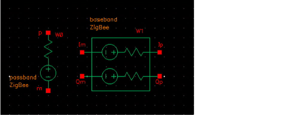
ZigBee modulation source
Command-line help
spectre -h wsource
Notes
zigbee applies ZigBee modulation compliant with IEEE Std 802.15.4-2006, Wireless Medium Access Control (MAC) and Physical Layer (PHY) Specifications for Low-Rate Wireless Personal Area Networks (WPANs). The present implementation is limited to the 2400 MHz band. zigbee netlists as a Spectre wsource.
The 2400 MHz band consists of 16 channels spaced by 5 MHz. The carrier frequency is given by Fc = 2405 + 5*(k-11) MHz.
k is the channel index in the range [11:26]. The parameter Channel determines the value of k.
You can reference Fc in the schematic and analysis dialogs as <instance_name>_wfreq, where <instance_name> is the schematic instance name of the zigbee cell.
A ZigBee frame consists of HeaderLength + DataLength octets (bytes), encoded in (HeaderLength + DataLength)*64 chips and transmitted at 2M chips/s. The duration of a frame is therefore Tframe = (HeaderLength + DataLength)*32 us.
The sampling frequency in the 2405M band is given by Fs = 4M*Oversample.
Oversample is a user-settable parameter.
CDF Parameters
Parameter Descriptions
- Signal type: Sets the passband or baseband operating mode.
- Signal type: Specifies the type of wsource in the design.
- Carrier harmonic: Specifies the carrier harmonic for the ZigBee source.
-
LO source type: Specifies the type of local oscillator. Possible values are
I&Qandsingle. This parameter is available only for the passband operating mode. - LO/I source name: Specifies the name of the local oscillator I path. This parameter is available only for the passband operating mode.
- LO/Q source name: Specifies the name of the local oscillator Q path. This parameter is available only for the passband operating mode.
- LO source name: Specifies the name of the local oscillator. This parameter is available only for the passband operating mode.
- Average Power: source available average power in dBm.
- Resistance: source Thevenin resistance.
-
Number of frames: The number of frames to simulate. The length of a frame is
(6 + Data length)*32u. -
Channel: Channel index
k. The channel index controls the carrier frequency, which is given byFc = 2405 + 5*(Channel–11) MHz. - PN code: The pseudo-random sequence that controls the data patterns.
- Data length: The number of data octets/bytes in the range [0:127]. Data length controls the length of a frame.
-
Oversample ratio: Controls the sampling frequency. The sampling frequency is given by
Oversample*4MHz. - SNR: Signal-to-noise power ratio.
Example
W0 (net2 net1) wsource standard="ZigBee" r=50 dbm=6.99 ZigBee_Channel=11 \ ZigBee_DataType=PN15 ZigBee_DataLength=20 oversample=3 framenumber=2
smartmeter
SYMBOL
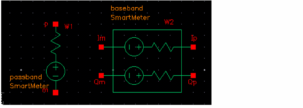
smartmeter modulation source
Command-line help
spectre -h wsource
Notes
smartmeter applies modulation compliant with IEEE Std 802.15.4g-2012. smartmeter netlists as a Spectre wsource.
smartmeter supports FSK Mode 1, OFDM Option 4, and OQPSK RateMode 3.
All frequency bands 0 through 13 as defined in Table 68f are supported.
A smart_meter frame consists of a header and data that depends on the modulation type, as set by the PHY Type parameter.
CDF Parameters For All Modulation Types
Parameter Descriptions For All Modulation Types
- Signal type: Sets the passband or baseband operating mode.
- Signal type: Specifies the type of wsource in the design.
- Carrier harmonic: Specifies the carrier harmonic for the smartmeter source.
-
LO source type: Specifies the type of local oscillator. Possible values are
I&Qandsingle. This parameter is available only for the passband operating mode. - LO/I source name: Specifies the name of the local oscillator I path. This parameter is available only for the passband operating mode.
- LO/Q source name: Specifies the name of the local oscillator Q path. This parameter is available only for the passband operating mode.
- LO source name: Specifies the name of the local oscillator. This parameter is available only for the passband operating mode.
- Average Power: Source available average power in dBm.
- Resistance: source Thevenin resistance.
- Number of frames: Number of frames to simulate.
- PN code: Sets the length of the shift register for the pseudo-random sequence that generates the data patterns.
- Oversample ratio: Controls the sampling frequency. Use the default of 4 for most simulations. If exceptionally wide bandwidth is needed in the PSD, set the parameter to 8.
- SNR: Signal-to-noise power ratio.
CDF Parameters for FSK
Parameter Descriptions for FSK
- Frequency band identifier: Sets the frequency band number from table 68f. Possible values for FSK are 0 through 13.
- Channel number: Channel numbers as defined in Table 68d are supported.
- Preamble length in octets: Preamble length as defined in Table 71. As per the table, values from 4 through 1000 are supported.
- Payload length in octets: Size of the data portion in octets. Values from 1 through 2047 are supported.
CDF Parameters for OFDM
Parameter Descriptions for OFDM
- Frequency band identifier: Sets the frequency band number from table 68f. Possible values for OFDM are 2, 3, 4, 7, 8, 9, 11, or 13.
- Channel number: Channel numbers as defined in Table 68d are supported.
- Number of data symbols: Number of OFDM data symbols in one frame.
- Modulation and coding: MCS 2 through 6 are implemented. Only OFDM Option 4 is supported.
- EVM measurement type: Values can be Data&Pilot, Data, or Pilot.
CDF Parameters for OQPSK
Parameter Descriptions for OQPSK
- Frequency band identifier: Sets the frequency band number from table 68f. The only possible value for OQPSK is 13.
- Channel number: Channel numbers as defined in Table 68d are supported.
- Payload length in octets: Size of the data portion in octets.
Examples
FSK (net2 0) wsource standard="SmartMeter" r=50 dbm=6.99 framenumber=3 \
oversample=4 SmartMeter_Channel=0 SmartMeter_DataType=PN9 \
SmartMeter_PHYType=FSK \
SmartMeter_Band=0 SmartMeter_PreambleLength=4 \
SmartMeter_DataLength=1000
OFDM (net2 0) wsource standard="SmartMeter" r=50 dbm=6.99 framenumber=3 \
oversample=4 SmartMeter_Channel=0 SmartMeter_DataType=PN9 \
SmartMeter_PHYType=OFDM \
SmartMeter_Band=2 SmartMeter_DataSym=80 SmartMeter_MCS=2 \
SmartMeter_EVMType=Data&Pilot
OQPSK (net2 0) wsource standard="SmartMeter" r=50 dbm=6.99 framenumber=3 \
oversample=4 SmartMeter_Channel=0 SmartMeter_DataType=PN9 \
SmartMeter_PHYType=OQPSK \
SmartMeter_Band=13 SmartMeter_DataLength=1000
DMR
Symbol
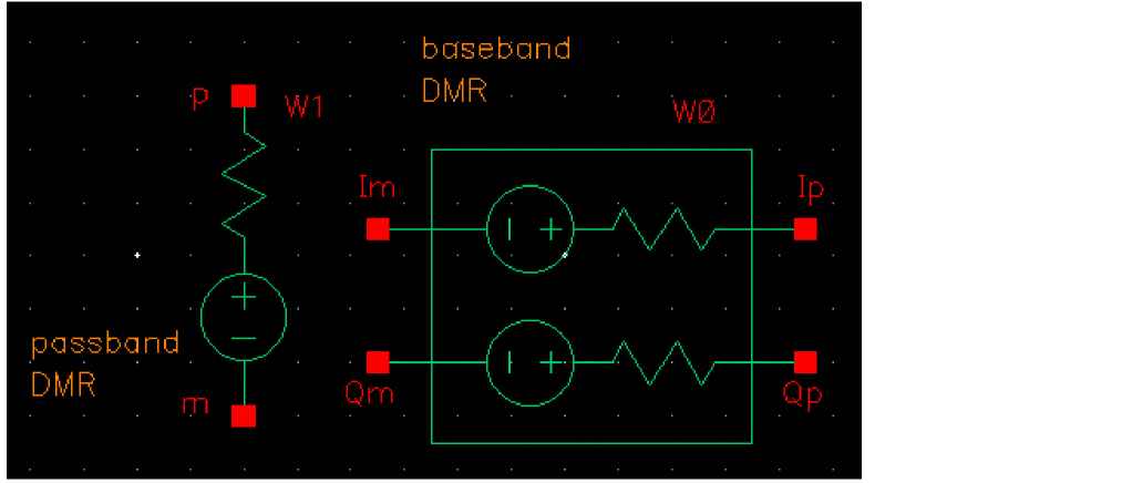
DMR Modulation Source
Command-line Help
spectre -h wsource
Notes
DMR netlists as a Spectre wsource.
The carrier frequency is in the 30MHz to 1GHz band. As always, you can reference the carrier frequency in the schematic and analysis dialogs as <instance_name>_wfreq, where <instance_name> is the schematic instance name of the DMR cell.
DMR operates within a 12.5 KHz RF carrier bandwidth.
Parameter Descriptions
- Signal type: Sets the passband or baseband operating mode.
- Source type: Specifies the type of wsource in the design.
- Carrier harmonic: Specifies the carrier harmonic for the NR source.
-
LO source type: Specifies the type of local oscillator. Possible values are
I&Qandsingle. This parameter is available only for the passband operating mode. - LO/I source name: Specifies the name of the local oscillator I path. This parameter is available only for the passband operating mode.
- LO/Q source name: Specifies the name of the local oscillator Q path. This parameter is available only for the passband operating mode.
- LO source name: Specifies the name of the local oscillator. This parameter is available only for the passband operating mode.
- Average Power: Source available average power in dBm.
- Resistance: source Thevenin resistance in Ohms.
- Number of bursts: The number of frames to simulate. Default is 1.
- Oversample ratio: Controls the sampling frequency. The default is 4.
- SNR: Signal-to-noise power ratio.
- Carrier frequency: Channel center frequency, in range [30M:1G].
- PN Code: The pseudo random sequence for the transmitted data. Possible values are PN9, PN15, and PN23.
- Pulse shaping filter type: Pulse shaping filter type. Possible values are None and RRC.
- Roll-off factor: Roll-off factor, in range (0:1).
- Idle time: Idle time in a TDMA frame. Possible values are 0 and 30m.
Example
W0 (net2 net1) wsource standard="DMR" r=50 dbm=6.99 DMR_Frequency=200M DMR_Alpha=0.1 DMR_IdleTime=30M
WLAN11A
SYMBOL
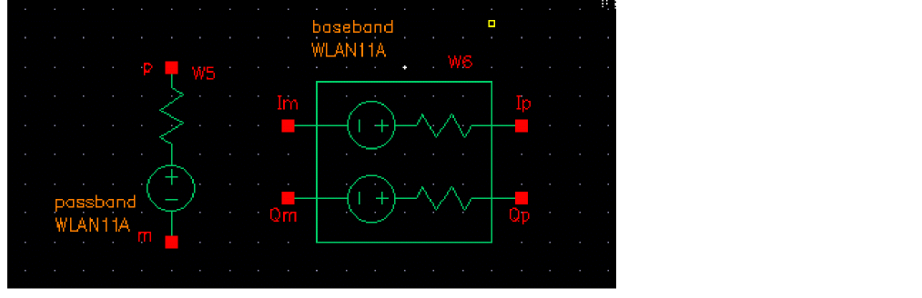
802.11a modulation source
Command-line help
spectre -h wsource
Notes
wlan11a applies 802.11a-compliant modulation according to IEEE Standard 802.11a-1999, Wireless LAN Medium Access Control (MAC) and Physical Layer (PHY) specifications, High-Speed physical Layer in the 5 GHz Band.
wlan11a netlists as a Spectre wsource.
The carrier frequency is in the 5 GHz band. As always, you can reference the carrier frequency in the schematic and analysis dialogs as <instance_name>_wfreq, where <instance_name> is the schematic instance name of the wlan11a cell.
A wlan11a frame consists of preamble and data. Data length is a settable property with a default of 20 symbols. The frame duration and sampling frequencies are given in the table below assuming 20 data symbols.
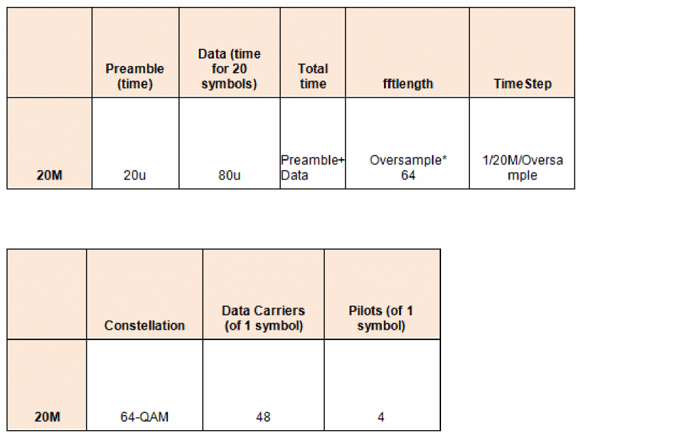
CDF Parameters
Note: 802.11a is 802.11n in the 5GHz frequency band with the long guard interval using legacy format and fixed bandwidth of 20MHz. 802.11a netlists as 802.11n with the appropriate settings.
Parameter Descriptions
- Signal type: Sets the passband or baseband operating mode.
- Signal type: Specifies the type of wsource in the design.
- Carrier harmonic: Specifies the carrier harmonic for the wlan11a source.
-
LO source type: Specifies the type of local oscillator. Possible values are
I&Qandsingle. This parameter is available only for the passband operating mode. - LO/I source name: Specifies the name of the local oscillator I path. This parameter is available only for the passband operating mode.
- LO/Q source name: Specifies the name of the local oscillator Q path. This parameter is available only for the passband operating mode.
- LO source name: Specifies the name of the local oscillator. This parameter is available only for the passband operating mode.
- Average Power: Source available average power in dBm.
- Resistance: source Thevenin resistance in Ohms.
- Number of frames: The number of frames to simulate. Refer to the table for the frame Oversample: Controls the sampling frequency. Refer to the table for details.
- Oversample: Controls the sampling frequency. The default is 4.
- SNR: Signal-to-noise power ratio.
-
Channel number: Channel number in range [0:200] in the 5GHz band. The carrier frequency is given by
Fc (MHz) = 5000 + 5*WLAN11N_Channel. -
EVM measurement type: EVM measurement type. When set to
Data&Pilot, the EVM calculation includes all the used subcarriers of Data and Pilots. When set toData, the EVM calculation includes only the Data subcarriers. When set toPilot, the EVM calculation includes only the Pilot subcarriers. Possible values areData&Pilot,Data, andPilot.
Example
W0 (net2 net1) wsource standard="WLAN11N" r=50 dbm=6.99 WLAN11N_Mode=Legacy \ WLAN11N_Bandwidth=20M WLAN11N_Oversample=4 WLAN11N_GI=Long framenumber=1 WLAN_11N_Channel=100 WLAN_11NDataSym=20
WLAN11P
SYMBOL
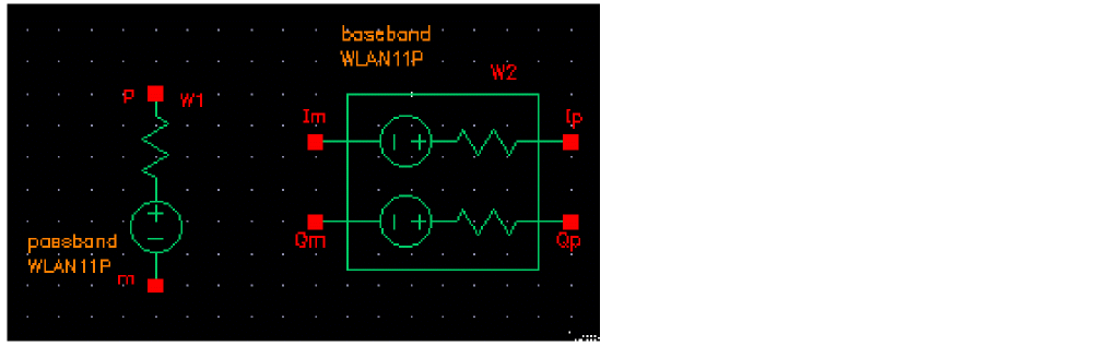
802.11p modulation source
Command-line help
spectre -h wsource
Notes
wlan11p applies 802.11p-compliant modulation according to IEEE Standard 802.11p-2010, Wireless LAN Medium Access Control (MAC) and Physical Layer (PHY) specifications.
wlan11p netlists as a Spectre wsource.
The carrier frequency is in the 5 GHz or 700 MHz band. As always, you can reference the carrier frequency in the schematic and analysis dialogs as <instance_name>_wfreq, where <instance_name> is the schematic instance name of the wlan11p cell.
A wlan11p frame consists of preamble and data. The Data length property can be set with a default of 80 symbols. The frame duration and sampling frequencies are given in the table below assuming 80 data symbols.
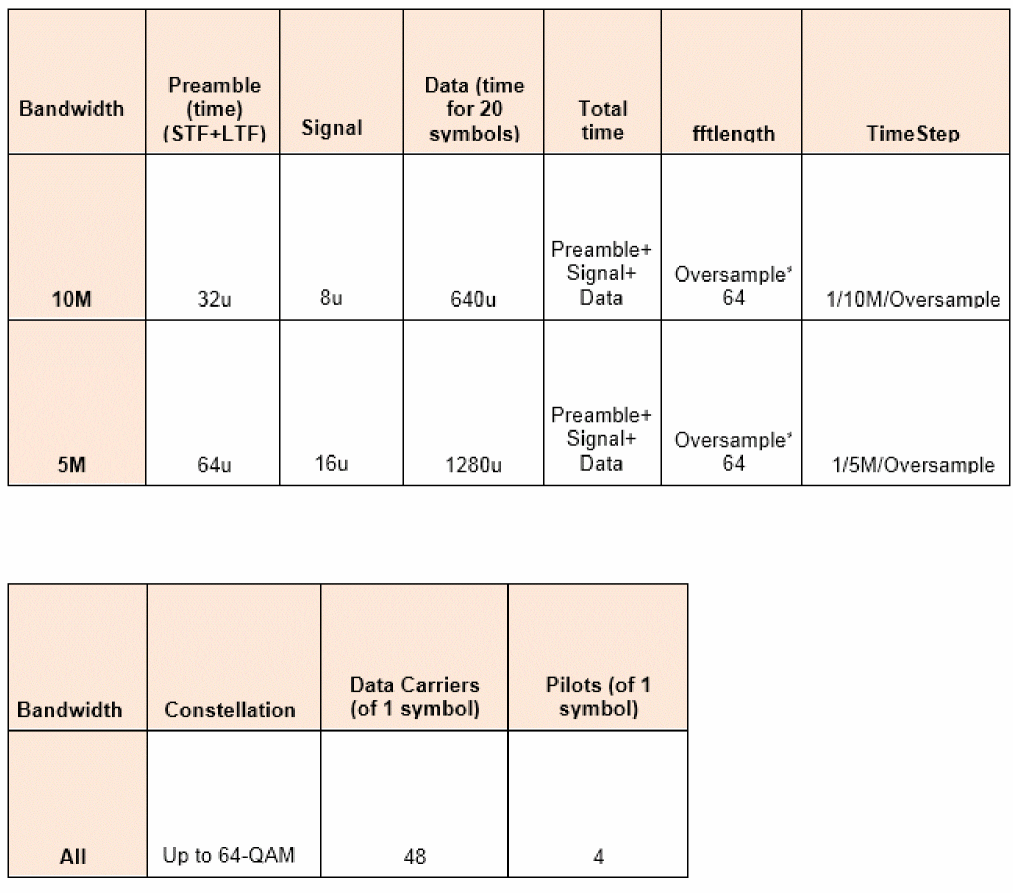
CDF Parameters
Parameter Descriptions
- Signal type: Sets the type of operating band.
- Source type: Specifies the type of wsource in the design.
- Carrier harmonic: Specifies the carrier harmonic for the wlan11p source.
-
LO source type: Specifies the type of local oscillator. Possible values are
I&Qandsingle. This parameter is available only for the passband operating mode. - LO/I source name: Specifies the name of the local oscillator I path. This parameter is available only for the passband operating mode.
- LO/Q source name: Specifies the name of the local oscillator Q path. This parameter is available only for the passband operating mode.
- LO source name: Specifies the name of the local oscillator. This parameter is available only for the passband operating mode.
- Average Power: Source available average power in dBm.
- Resistance: Source Thevenin resistance in Ohms.
- Number of frames: The number of frames to simulate.
- Oversample: Controls the sampling frequency. The default is 4.
- SNR: Signal-to-noise power ratio.
- Band: Frequency band. Possible values are 5G or 700M.
- Bandwidth: Channel Bandwidth for the 5G band. Can be set to 5M or 10M. For 20M bandwidth, use the wlan11a source.
-
Channel number: Channel number in range [170:184] in the 5GHz band. For the 10MHz channel bandwidth, the carrier frequency is given by
Fc (MHz) = 5000 + 5*WLAN11P_Channel. For the 5MHz channel bandwidth, the carrier frequency is given byFc (MHz) = 5002.5 + 5*WLAN11P_Channel. - PN Code: Pseudo-random code shift register length. Default is PN9. PN15 and PN23 are also available.
- Number of data symbols: Default is 80.
- Modulation Coding Scheme: Default is 7. MCS 0 and 1 are bpsk. MCS 2 and 3 are qpsk. MCS 4 and 5 are 16-QAM. MCS 6 and 7 are 64-QAM. Note that coding is not supported. Coding is used for error detection and correction. All the bits are treated as data bits.
-
EVM measurement type: When set to
Data&Pilot, the EVM calculation includes all the used subcarriers of Data and Pilots. When set toData, the EVM calculation includes only the Data subcarriers. When set toPilot, the EVM calculation includes only the Pilot subcarriers. Possible values areData&Pilot,Data, andPilot.
In the ADE Direct Plot functions, the spectral mask follows 802.11p-2010 Table I.7. Power Class C is adopted.
Example
W0 (net2 net1) wsource standard="WLAN11P" r=50 dbm=6.99 WLAN11P_Bandwidth=10M WLAN11P_Oversample=4 framenumber=1 WLAN_11P_Channel=174 WLAN_11PDataSym=80
WLAN11N
SYMBOL
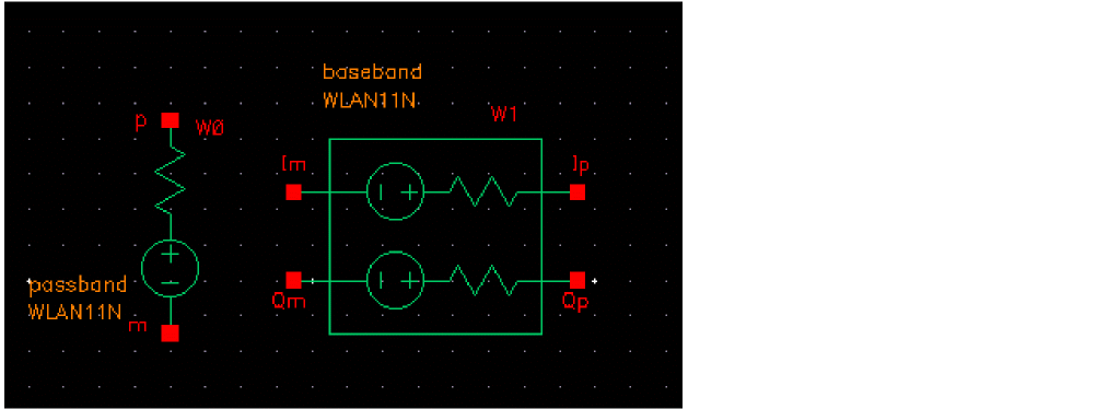
802.11n modulation source
Command-line help
spectre -h wsource
Notes
wlan11n applies 802.11n-compliant modulation according to IEEE Standard 802.11n-2009, Wireless LAN Medium Access Control (MAC) and Physical Layer (PHY) specifications, Amendment 5: Enhancements for Higher Throughput.
wlan11n netlists as a Spectre wsource.
The carrier frequency is selectable to be in the 2.4GHz or 5 GHz band. As always, you can reference the carrier frequency in the schematic and analysis dialogs as <instance_name>_wfreq, where <instance_name> is the schematic instance name of the wlan11n cell.
A wlan11n frame consists of preamble and data. Data length is settable with a property on the schematic symbol. The frame duration and sampling frequencies are given in the table below.
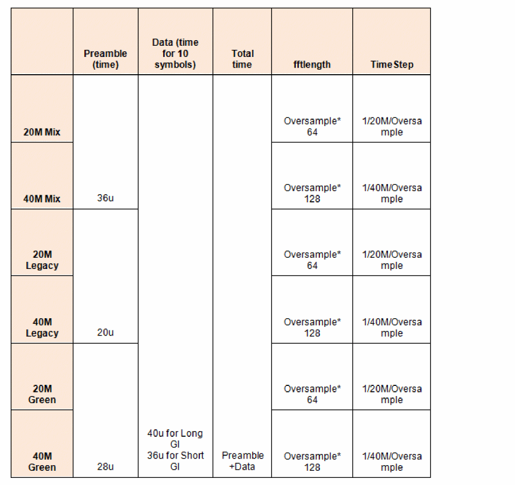
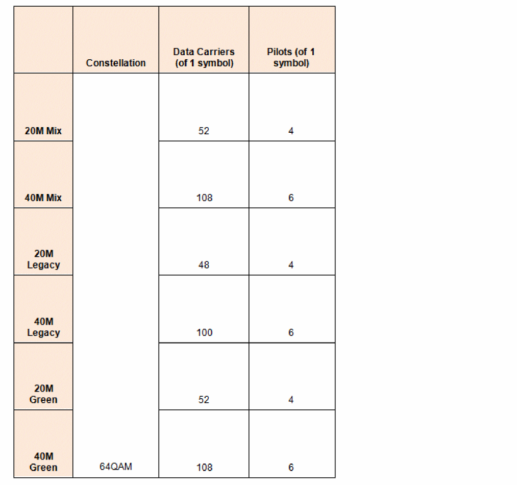
CDF Parameters
Parameter Descriptions
- Signal type: Sets the passband or baseband operating mode.
- Source type: Specifies the type of wsource in the design.
- Carrier harmonic: Specifies the carrier harmonic for the wlan11n source.
-
LO source type: Specifies the type of local oscillator. Possible values are
I&Qandsingle. This parameter is available only for the passband operating mode. - LO/I source name: Specifies the name of the local oscillator I path. This parameter is available only for the passband operating mode.
- LO/Q source name: Specifies the name of the local oscillator Q path. This parameter is available only for the passband operating mode.
- LO source name: Specifies the name of the local oscillator. This parameter is available only for the passband operating mode.
- Average Power: Source available average power in dBm.
- Resistance: source Thevenin resistance in Ohms.
- Number of frames: The number of frames to simulate. Refer to the table for the frame structure and details.
- PHY format: Choice of Mix, Green, or Legacy.
- Bandwidth: Choice of 20 MHz or 40 MHz bandwidth.
- Frequency band: Choice of 2.4G or 5G band.
- Oversample: Controls the sampling frequency. Refer to the table for details.
- Guard interval: Choice of Long and Short guard interval.
- SNR: Signal-to-noise power ratio.
-
Channel number: Channel number in range [0:200]. For the 5GHz band, the carrier frequency is given by
Fc (MHz) = 5000 + 5*WLAN11N_Channel. For the 2.4GHz band, it is given byFc (MHz) = 2407+ 5*WLAN11N_Channel. -
EVM measurement type: EVM measurement type. When set to
Data&Pilot, the EVM calculation includes all the used subcarriers of Data and Pilots. When set toData, the EVM calculation includes only the Data subcarriers. When set toPilot, the EVM calculation includes only the Pilot subcarriers. Possible values areData&Pilot,Data, andPilot.
Example
W0 (net2 net1) wsource standard="WLAN11N" r=50 dbm=6.99 WLAN11N_Mode=Mix \ WLAN11N_Bandwidth=20M oversample=4 WLAN11N_GI=Long framenumber=1
WLAN11AC
SYMBOL
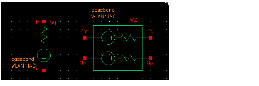
802.11ac modulation source
Command-line help
spectre -h wsource
Notes
wlan11ac applies 802.11ac-compliant modulation according to IEEE Standard 802.11ac-2013, Wireless LAN Medium Access Control (MAC) and Physical Layer (PHY) specifications, Amendment 4: Enhancements for Very High Throughput for Operation in Bands below 6GHz.
wlan11ac netlists as a Spectre wsource.
The carrier frequency is in the 5 GHz band. As always, you can reference the carrier frequency in the schematic and analysis dialogs as <instance_name>_wfreq, where <instance_name> is the schematic instance name of the wlan11ac cell.
A wlan11ac frame consists of preamble and data. Data length is settable with a property with a default of 80 symbols. The frame duration and sampling frequencies are given in the table below assuming 80 symbols.
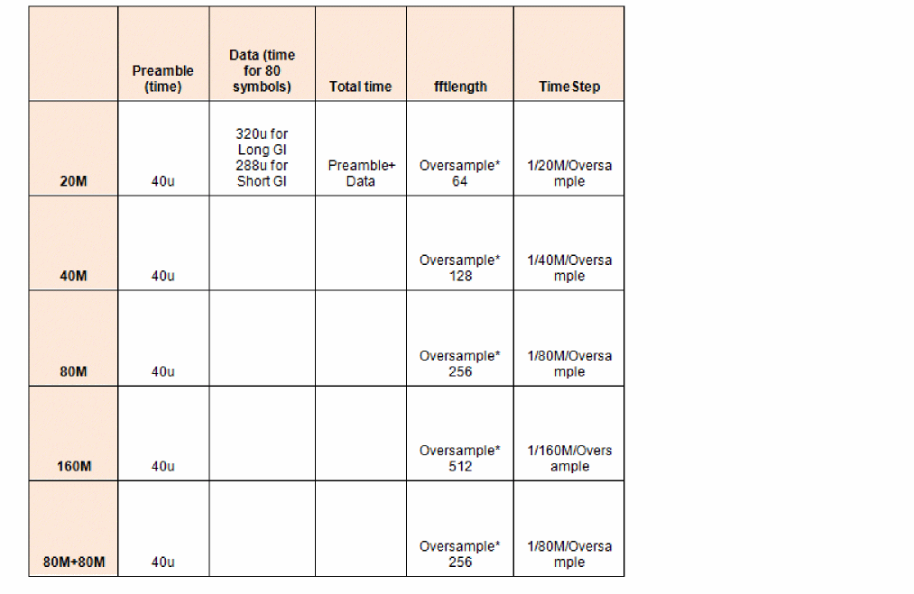
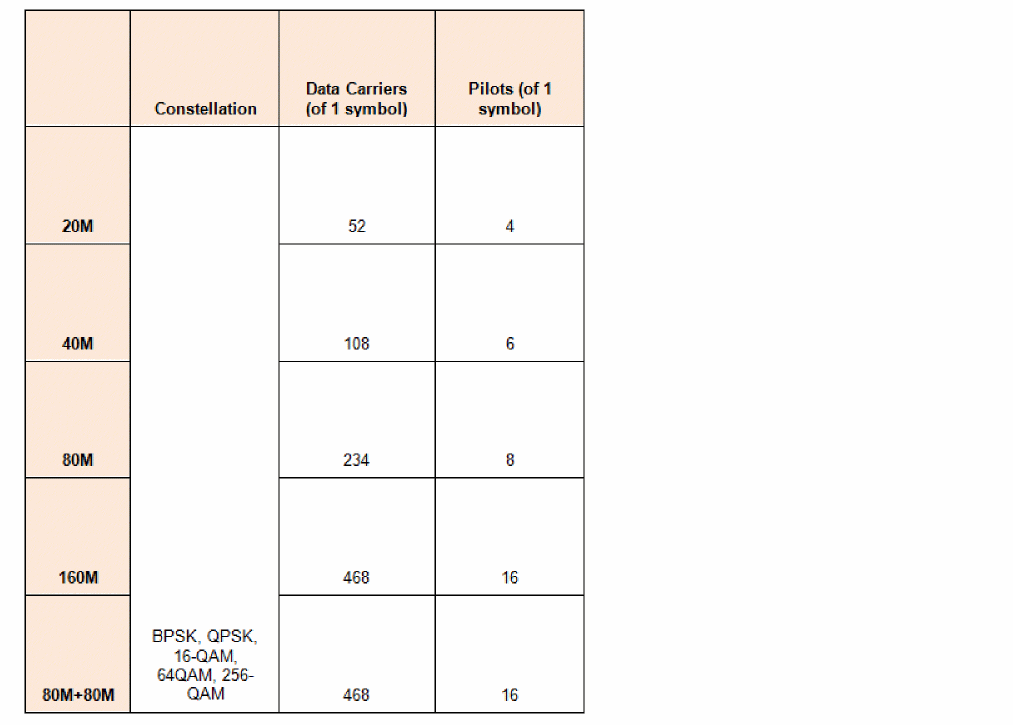
CDF Parameters
Parameter Descriptions
- Signal type: Sets the passband or baseband operating mode.
- Source type: Specifies the type of wsource in the design.
- Carrier harmonic: Specifies the carrier harmonic for the wlan11ac source.
-
LO source type: Specifies the type of local oscillator. Possible values are
I&Qandsingle. This parameter is available only for the passband operating mode. - LO/I source name: Specifies the name of the local oscillator I path. This parameter is available only for the passband operating mode.
- LO/Q source name: Specifies the name of the local oscillator Q path. This parameter is available only for the passband operating mode.
- LO source name: Specifies the name of the local oscillator. This parameter is available only for the passband operating mode.
- Average Power: Source available average power in dBm.
- Resistance: Source Thevenin resistance in Ohms.
- Number of frames: The number of frames to simulate. Refer to the table for the frame structure and details.
- Bandwidth: Choice of 20M, 40M, 80M, 160M, or 80+80M bandwidth.
- Modulation coding scheme: 0 through 9 are selectable.
- Oversample: Controls the sampling frequency. Refer to the table for details.
- Guard interval: Choice of Long and Short guard interval.
- SNR: Signal-to-noise power ratio.
-
Channel number: Channel number in range [0:200]. The carrier frequency is given by
Fc (MHz) = 5000 + 5*WLAN11N_Channel. - PN code: This sets the length of the shift register in the pseudorandom number generator to generate the data bits. The default is PN23 and is strongly suggested. PN23, PN15, and PN9 are available.
-
EVM measurement type: EVM measurement type. When set to
Data&Pilot, the EVM calculation includes all the used subcarriers of Data and Pilots. When set toData, the EVM calculation includes only the Data subcarriers. When set toPilot, the EVM calculation includes only the Pilot subcarriers. Possible values areData&Pilot,Data, andPilot.
Example
W0 (net2 net1) wsource standard="WLAN11AC" r=50 dbm=6.99 WLAN11AC_MCS=8 \ WLAN11AC_Bandwidth=80M oversample=4 WLAN11AC_GI=Long framenumber=1
WLAN11AD
SYMBOL
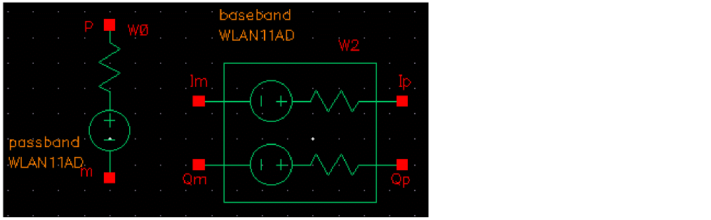
802.11ad modulation source
Command-line help
spectre -h wsource
Notes
wlan11ad applies 802.11ad-compliant modulation according to IEEE Standard 802.11ad-2012, Wireless LAN Medium Access Control (MAC) and Physical Layer (PHY) specifications, Amendment 3: Enhancements for Very High Throughput in the 60GHz band.
wlan11ad netlists as a Spectre wsource.
The carrier frequency is in the 60 GHz band range. As always, you can reference the carrier frequency in the schematic and analysis dialogs as <instance_name>_wfreq, where <instance_name> is the schematic instance name of the wlan11ad cell.
A root-raised cosine (RRC) filter with roll-off factor in the range (0:1) can be chosen. Default is 0.25. The impulse response of RRC filter is given by:
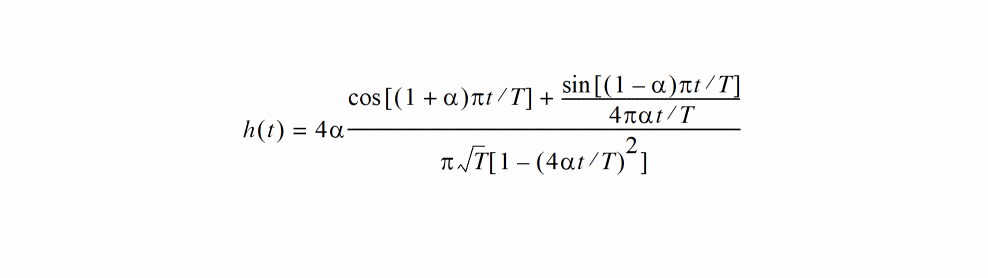
where T is the symbol period and ![]() is the roll-off factor.
is the roll-off factor.
The length of impulse response of the filter is given by:
where span is the filter span in symbols and oversample is the output samples per symbol.
A wlan11ad frame consists of preamble, header, and data. Details are provided in the table below.
CDF Parameters
Parameter Descriptions
- Signal type: Sets the passband or baseband operating mode.
- Source type: Specifies the type of wsource in the design.
- Carrier harmonic: Specifies the carrier harmonic for the wlan11ad source.
-
LO source type: Specifies the type of local oscillator. Possible values are
I&Qandsingle. This parameter is available only for the passband operating mode. - LO/I source name: Specifies the name of the local oscillator I path. This parameter is available only for the passband operating mode.
- LO/Q source name: Specifies the name of the local oscillator Q path. This parameter is available only for the passband operating mode.
- LO source name: Specifies the name of the local oscillator. This parameter is available only for the passband operating mode.
- Average Power: Source available average power in dBm.
- Resistance: Source Thevenin resistance in Ohms.
- Number of frames: The number of frames to simulate. Refer to the table for the frame structure and details.
- Oversample ratio: Controls the sampling frequency.
- SNR: Signal-to-noise power ratio.
-
Channel number: Channel number in range [1:4]. The carrier frequency is given by
Fc (GHz) = 56.16 + 2.16*WLAN11N_Channel. - Modulation and coding scheme: 0 through 24 are selectable.
- Number of data symbols: The number of data symbols. Default is 80. This option is visible only when MCS is in the range [13:24].
-
EVM measurement type: EVM measurement type. When set to
Data&Pilot, EVM calculation includes all the used subcarriers of Data and Pilots. When set toData, EVM calculation includes only the Data subcarriers. When set toPilot, EVM calculation includes only the Pilot subcarriers. Possible values areData&Pilot,Data, andPilot. This option is visible only when MCS is in the range [13:24]. - Data length in octets: Sets the length of the data portion of the frame in octets. This option is visible only when MCS in the range [0:12]
- Pulse shaping filter type: Sets the pulse shaping filter type. Possible values are RRC and none. This option is visible only when MCS is in the range [0:12].
- Roll-off factor: Roll-off factor for the RRC filter.
Example
W0 (net2 net1) wsource standard="WLAN11AD" r=50 dbm=6.99 WLAN11AD_MCS=8 \ oversample=4 WLAN11AD_FilterType=RRC
WLAN11AF
SYMBOL
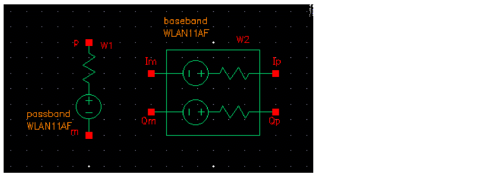
802.11af modulation source
Command-line help
spectre -h wsource
Notes
wlan11af applies 802.11af-compliant modulation according to IEEE Standard 802.11af-2013, Wireless LAN Medium Access Control (MAC) and Physical Layer (PHY) specifications, Amendment 5: TV White Spaces Operation.
wlan11af netlists as a Spectre wsource.
The carrier frequency is in the television white space frequency range. As always, you can reference the carrier frequency in the schematic and analysis dialogs as <instance_name>_wfreq, where <instance_name> is the schematic instance name of the wlan11af cell.
A wlan11af frame consists of preamble and data. Data length is settable with a property with a default of 80 symbols. The frame duration and sampling frequencies are given in the table below assuming 80 symbols.
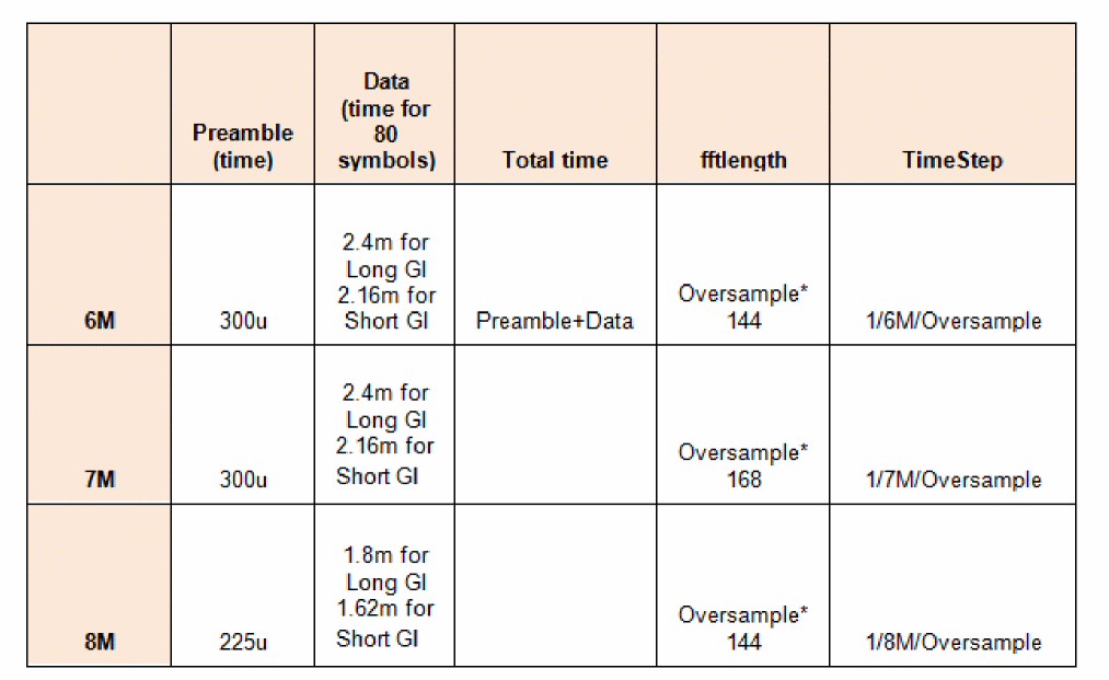
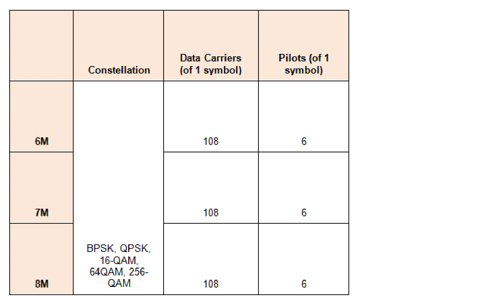
CDF Parameters
Parameter Descriptions
- Signal type: Sets the passband or baseband operating mode.
- Source type: Specifies the type of wsource in the design.
- Carrier harmonic: Specifies the carrier harmonic for the wlan11af source.
-
LO source type: Specifies the type of local oscillator. Possible values are
I&Qandsingle. This parameter is available only for the passband operating mode. - LO/I source name: Specifies the name of the local oscillator I path. This parameter is available only for the passband operating mode.
- LO/Q source name: Specifies the name of the local oscillator Q path. This parameter is available only for the passband operating mode.
- LO source name: Specifies the name of the local oscillator. This parameter is available only for the passband operating mode.
- Average Power: Source available average power in dBm.
- Resistance: Source Thevenin resistance in Ohms.
- Number of frames: The number of frames to simulate. Refer to the table for the frame structure and details.
- Bandwidth: Choice of 6 MHz, 7 MHz, or 8 MHz bandwidth.
- Modulation coding scheme: 0 through 9 are selectable.
- Oversample: Controls the sampling frequency. Refer to the table for details.
- Guard interval: Choice of Long and Short guard interval.
- SNR: Signal-to-noise power ratio.
-
Channel number: Channel number in range [2:51]. The carrier frequency is given by
StartingFreq + ChNum*6Mwhere the StartingFreq is 45MHz for channels 2 through 4, 49MHz for channels 5 and 6, 99MHz for channels 7 through 13, and 389MHz for channels 14 through 51. - PN code: This sets the length of the shift register in the pseudorandom number generator to generate the data bits. The default is PN23 and is strongly suggested. PN23, PN15, and PN9 are available.
-
EVM measurement type: EVM measurement type. When set to
Data&Pilot, the EVM calculation includes all the used subcarriers of Data and Pilots. When set toData, the EVM calculation includes only the Data subcarriers. When set toPilot, the EVM calculation includes only the Pilot subcarriers. Possible values areData&Pilot,Data, andPilot. - Carrier freq for 7M/8M BW: When the bandwidth is 7MHz or 8MHz, the carrier frequency must be specified.
Example
W0 (net2 net1) wsource standard="WLAN11AF" r=50 dbm=6.99 WLAN11AF_MCS=8 \ WLAN11AF_Bandwidth=6M oversample=4 WLAN11AF_GI=Long framenumber=1
WLAN11AH
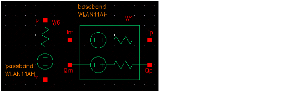
802.11ah modulation source
Command-line help
spectre -h wsource
Notes
wlan11ah applies 802.11ah-compliant modulation that is an amendment of the IEEE 802.11-2007 wireless networking standard.
wlan11ah netlists as a Spectre wsource.
The carrier frequency is set in the Carrier frequency field in the property list. An ADE variable W0_wfreq (where W0 is the instance name of the wireless source) is introduced with a default value of 1G in the ADE variables section. The value set in ADE is not used. Instead, this variable is assigned at the beginning of the simulation to the value specified in the Carrier frequency field.
The WLAN11AH standard offers three modes: 1 MHz (S1G_1M), long preamble mode (S1G_LONG), and short preamble mode (S1G_SHORT).
A wlan11ah frame consists of preamble and data. The frame duration and sampling frequencies are given in the table below assuming 80 symbols.
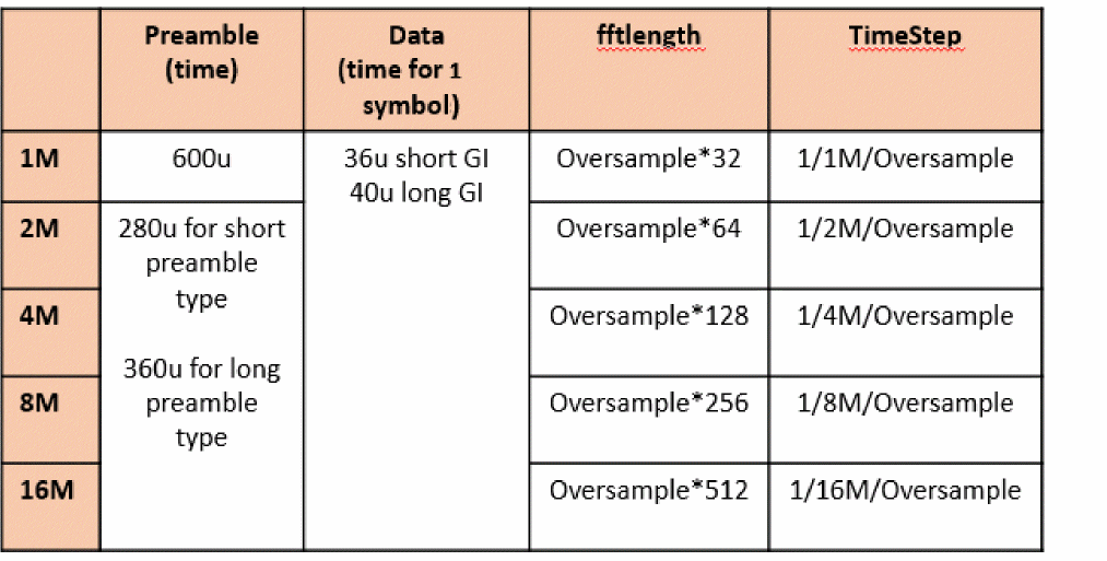
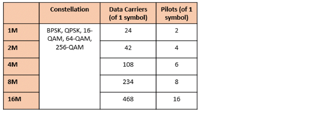
CDF Parameters
Parameter Descriptions
- Signal type: Sets the passband or baseband operating mode.
- Source type: Specifies the type of wsource in the design.
- Carrier harmonic: Specifies the carrier harmonic for the wlan11ah source.
-
LO source type: Specifies the type of local oscillator. Possible values are
I&Qandsingle. This parameter is available only for the passband operating mode. - LO/I source name: Specifies the name of the local oscillator I path. This parameter is available only for the passband operating mode.
- LO/Q source name: Specifies the name of the local oscillator Q path. This parameter is available only for the passband operating mode.
- LO source name: Specifies the name of the local oscillator. This parameter is available only for the passband operating mode.
- Average Power: Source available average power in dBm.
- Resistance: Source Thevenin resistance in Ohms.
- Number of frames: The number of frames to simulate. Refer to the table for the frame structure and details.
- Oversample ratio: Controls the sampling frequency. Refer to the table for details.
- SNR: Signal-to-noise power ratio.
- Carrier Frequency: Channel center frequency in the range (700M: 1G).
- PN code: This sets the length of the shift register in the pseudorandom number generator to generate the data bits. The default is PN23 and is strongly suggested. PN23, PN15, and PN9 are available.
- Number of data symbols: Number of PSDU data symbols in each frame.
- Bandwidth: Choice of 1MHz, 2 MHz, 4 MHz, 8 MHz, or 16MHz bandwidth.
- Modulation coding scheme: 0 through 9 are selectable.
- Guard interval: Choice of Normal and Short guard intervals.
-
EVM measurement type: EVM measurement type. When set to
Data&Pilot, the EVM calculation includes all the used subcarriers of Data and Pilots. When set toData, the EVM calculation includes only the Data subcarriers. When set toPilot, the EVM calculation includes only the Pilot subcarriers. Possible values areData&Pilot,Data, andPilot. - Preamble type: Sets the preamble type Short or Long for the 2 MHz, 4 MHz, 8 MHz, or 16 MHz bandwidth.
Example
W0 (net2 net1) wsource standard="WLAN11AH" r=50 dbm=6.99 WLAN11AH_MCS=8 \ WLAN11AH_Bandwidth=8M oversample=4 framenumber=1
WLAN11AX
Symbol
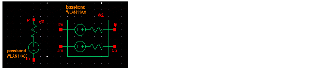
802.11ax modulation source
Command-line help
spectre -h wsource
Notes
wlan11ax netlists as a Spectre wsource.
Frequency Band
The 2.4GHz, 5GHz, and 6GHz ISM bands are used.
Frame Structure
A wlan11ax frame consists of preamble and data. Data length is settable with a property with a default of 80 symbols. The frame duration and sampling frequencies are given in the table below.
| Preamble (time) | Data time (Per Symbol) Excludes guard interval | FFT Length | Time Step | Total Time 80 symbols, G1 | Total time 80 symbols GI4 | |
| Constellation | Data Carriers of 1 Symbol | Pilot Carriers | |
|---|---|---|---|
CDF Parameters
| Label | Parameter | Type | Default |
- Signal type: Sets the passband or baseband operating mode.
- Source type: Specifies the type of wsource in the design.
- Carrier harmonic: Specifies the carrier harmonic for the wlan11ax source.
-
LO source type: Specifies the type of local oscillator. Possible values are
I&Qandsingle. This parameter is available only for the passband operating mode. - LO/I source name: Specifies the name of the local oscillator I path. This parameter is available only for the passband operating mode.
- LO/Q source name: Specifies the name of the local oscillator Q path. This parameter is available only for the passband operating mode.
- LO source name: Specifies the name of the local oscillator. This parameter is available only for the passband operating mode.
- Average Power: Source available average power in dBm.
- Resistance: Source Thevenin resistance in Ohms.
- Number of frames: The number of frames to simulate. Refer to the table for the frame structure and details.
- Oversample ratio: Controls the sampling frequency. Refer to the table for details.
- SNR: Signal-to-noise power ratio.
- Frequency Band: Choice of 2.4GHz, 5GHz, and 6GHz ISM bands.
-
Channel number: Channel number. For 5G band, the carrier frequency is given by
Fc (MHz) = 5000 + 5*WLAN11N_Channel. For 2.4G band, the carrier frequency is given byFc (MHz) = 2407 + 5*WLAN11N_Channel. For 6G band, it is given byFc = 5925 + 5*WLAN11N_Channel. - PN code: This sets the length of the shift register in the pseudorandom number generator to generate the data bits. The default is PN23 and is strongly suggested. PN23, PN15, and PN9 are available.
- Bandwidth: Signal bandwidth. For 5G and 6G band, choice of 20M, 40M, 80M, 160M, or 80+80M bandwidth is available. For 2.4G band, 20M, 40M, or 80M bandwidth is available.
- Modulation coding scheme: 0 through 11 are selectable.
- Guard interval: Choice of GI1, GI2, and GI4 guard intervals. GI1 is 0.8usec. GI2 is 1.6usec. GI4 is 3.2usec.
-
EVM measurement type: EVM measurement type. When set to
Data&Pilot, the EVM calculation includes all the used subcarriers of Data and Pilots. When set toData, the EVM calculation includes only the Data subcarriers. When set toPilot, the EVM calculation includes only the Pilot subcarriers. Possible values areData&Pilot,Data, andPilot.
Example
W0 (net2 net1) wsource standard="WLAN11AX" r=50 dbm=6.99 WLAN11AX_MCS=8 \ WLAN11AX_Bandwidth=80M oversample=4 WLAN11AX_GI=GI1 framenumber=1
Bluetooth
SYMBOL
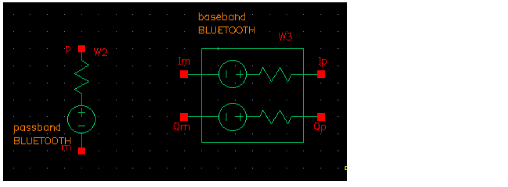
Bluetooth modulation source
Command-line help
spectre -h wsource
Notes
bluetooth applies Bluetooth LE and Bluetooth HS compliant modulation according to Covered Core Package Version 4.2, December 2014.
Bluetooth netlists as a Spectre wsource.
A Bluetooth LE frame consists of preamble, data, and CRC fields. Data length can be set using a property with a default of 10 octets. The frame duration is given in the table below assuming 10 octets.
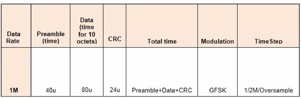
HS Mode
A Bluetooth HS frame consists of preamble, header, and data. Data length can be set using a property with a default of 10 octets for data rates of 1M, 2M, 5.5M, and 11M. For 72M, the default is 80 OFDM symbols. The frame duration is given in the table below assuming 10 octets for the 1M, 2M, 5.5M, and 11M data rates, and 80 OFDM symbols for the 72M rate.
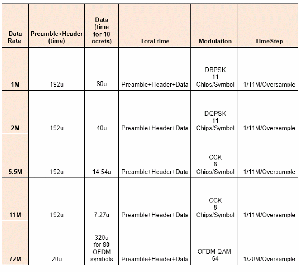
CDF Parameters
| Label | Parameter | Type | Default |
|
Data length in octets (LE Mode and HS Mode for 11M rate and below.) |
|||
Parameter Descriptions
- Signal type: Sets the passband or baseband operating mode.
- Source type: Specifies the type of wsource in the design.
- Carrier harmonic: Specifies the carrier harmonic for the bluetooth source.
-
LO source type: Specifies the type of local oscillator. Possible values are
I&Qandsingle. This parameter is available only for the passband operating mode. - LO/I source name: Specifies the name of the local oscillator I path. This parameter is available only for the passband operating mode.
- LO/Q source name: Specifies the name of the local oscillator Q path. This parameter is available only for the passband operating mode.
- LO source name: Specifies the name of the local oscillator. This parameter is available only for the passband operating mode.
- Average Power: Source available average power in dBm.
- Resistance: Source Thevenin resistance in Ohms.
- Number of frames: The number of frames to simulate. Refer to the table for the frame.
- Oversample: Controls the sampling frequency. Refer to the table for details.
- SNR: Signal-to-noise power ratio.
- Bluetooth mode: Sets the mode to LE, HS, EDR, or BR.
-
Channel number: Channel number. For LE mode, it is in the range [0:39] and the carrier frequency is given by
Fc (MHz) = 2402 + 2 * BLUETOOTH_Channel. For HS mode 72Mbps, it is in the range [1:13] and carrier frequency is given byFc (MHz) = 2407 + 5 * BLUETOOTH_Channel. For other data rate in HS mode, it is in the range [1:14] and the carrier frequency is given byFc (MHz) = 2407 + 5 * BLUETOOTH_Channelfor channel [1:13], andFc = 2484MHz for channel 14. For EDR and BR mode, it is in the range [0:78] and the carrier frequency is given byFc (MHz) = 2402 + BLUETOOTH_Channel. - PN code: This sets the length of the shift register in the pseudorandom number generator to generate the data bits. The default is PN9. PN23, PN15, and PN9 are available.
- Data length in octets: Data length in octets. For LE data channel, it is in the range [1:255]. For LE advertising channel (channel 0, 12, 39), it is in the range [6:37]. For HS mode, it is in the range [2:2e4] for simulation. For EDR mode, it is in the range [1:1021]. For BR mode, it is in the range [1:339].
-
Modulation type: Modulation type. Possible values are
FSKandGFSK. - Modulation index: Modulation index. For LE mode, it is in the range [0.45:0.55]. For BR mode, it is in the range [0.28:0.35].
- Data rate in bps: Data rate in bps for LE, HS and EDR modes. Possible values are 1M and 2M for LE mode; 1M, 2M, 5.5M, 11M and 72M for HS mode; 2M and 3M for EDR mode.
- Pulse shaping filter type: This sets the pulse shaping filter type for HS mode for 11M rate and below. Possible values are None and Gaussian.
- Bandwidth product: Sets the bandwidth time product for HS mode for 11M rage and below in the range (0 1].
- Number of data symbols: This sets the number of data symbols in the frame for HS 72M data rate mode.
-
EVM measurement type: When set to
Data&Pilot, the EVM calculation includes all the used subcarriers of Data and Pilots. When set toData, the EVM calculation includes only the Data subcarriers. When set toPilot, the EVM calculation includes only the Pilot subcarriers. Possible values areData&Pilot,Data, andPilot. This is available for HS mode 72M data rate only.
Example
W0 (net2 net1) wsource standard=”BLUETOOTH" r=50 dbm=6.99 \
BLUETOOTH_Mode=LE BLUETOOTH_Channel=2 BLUETOOTH_DataType=PN9 \
BLUETOOTH_DataLength=10 framenumber=1
Msource
SYMBOL
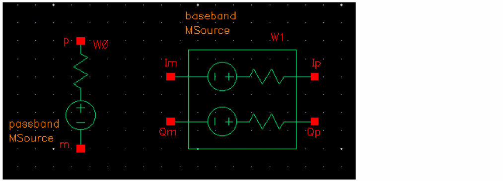
Msource modulation source
Command-line help
spectre -h wsource
Msource is a generic modulated source that can generate single carrier or OFDM modulated signals at any frequency and data rate.
Msource netlists as a Spectre wsource.
CDF Parameters
| Label | Parameter | Type | Default |
Parameter Descriptions
- Signal type: Sets the passband or baseband operating mode.
- Source type: Specifies the type of wsource in the design.
- Carrier harmonic: Specifies the carrier harmonic for the msource source.
-
LO source type: Specifies the type of local oscillator. Possible values are
I&Qandsingle. This parameter is available only for the passband operating mode. - LO/I source name: Specifies the name of the local oscillator I path. This parameter is available only for the passband operating mode.
- LO/Q source name: Specifies the name of the local oscillator Q path. This parameter is available only for the passband operating mode.
- LO source name: Specifies the name of the local oscillator. This parameter is available only for the passband operating mode.
- Average Power: Source available average power in dBm.
- Resistance: Source Thevenin resistance in Ohms.
- Number of frames: The number of frames to simulate.
- Oversample ratio: Controls the sampling frequency.
- SNR: Signal-to-noise power ratio.
- Channel frequency: The channel frequency in Hz.
- Data rate (bps): Data rate in bps.
-
Modulation type: Modulation type. Possible values are
BPSK,QPSK,M_8PSK,QAM16,QAM64,QAM256, andQAM1024. - Number of symbols: Number of symbols in a frame.
-
PN Code: This sets the length of the shift register in the pseudorandom number generator to generate the data bits. The default is
PN15. Other possible values arePN9andPN23. -
Pulse shaping filter type: Sets the pulse shaping filter type. Possible values are
NoneandRRC. -
Roll-off factor: The roll-off factor. The default value is
0.2. -
OFDM type: Sets the OFDM type. Possible values are
NoandYes. -
IFFT/FFT size: IFFT/FFT size. The default value is
64. -
Number of Data carriers: Sets the number of data carriers. The default value is
52. -
Cyclic prefix: Sets the cyclic prefix. Possible values are
1/4and1/8. The default value is1/4. -
Number of DC carriers: Number of DC carriers. Possible values are
1,3, and5. The default value is1.
Example
W0 (net2 net1) wsource standard=”msource" r=50 dbm=6.99 \
MSource_Frequency=5G MSource_Alpha=0.2 MSource_DataType=PN9 \
framenumber=1
WPROBE
SYMBOL
Wireless probe
Command-line help
spectre -h wprobe
Notes
wprobe serves the following two purposes:
-
In fast envelope wireless analysis mode,
wprobesets the output node. -
In both regular and fast envelope mode,
wprobeperforms signal post processing to calculate EVM, BER, and Spectrum measurements, including ACPR.
Electrically, wprobes are open-circuited.
wprobe provides output for three functions for use in the Direct Plot Form: Measure, Constellation, and Spectrum.
Measure
Measure provides the EVM and BER measurements. They are shown in the Direct Plot Form as <probe instance name>.evm and <probe instance name>.ber. Both are computed and plotted as functions of the frame index.
EVM measures the modulation accuracy of the transmitter. In order to calculate EVM, a time record of N received complex samples ![]() is captured. For each received complex sample,
is captured. For each received complex sample,
a decision is made about which complex value was transmitted. The error vector ![]() is defined as the distance from the ideal position (
is defined as the distance from the ideal position (Ij,Qj) to the actual position of the received point.
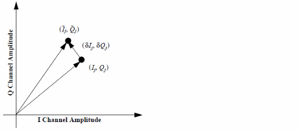
Therefore, the received vector is the sum of the ideal vector and the error vector, as shown below.
S is the magnitude of the vector to the ideal constellation.
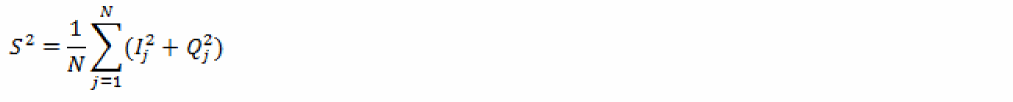
In digital transmission, the number of bit errors is the number of received bits of a data stream over a communication channel that have been altered due to noise, interference, distortion, or bit synchronization errors.
The bit error rate or bit error ratio (BER) is the number of bit errors divided by the total number of transferred bits during the simulated time interval. BER is a unitless performance measure, often expressed as a percentage.
Constellation
The Constellation function outputs two waveforms, <probe instance name>.mea and <probe instance name>.ref. <probe instance name>.mea plots ![]() , and the measured I/Q samples across the probe. The
, and the measured I/Q samples across the probe. The.ref measurement is the ideal reference signal from wsource.
Spectrum
The Spectrum measurement calculates the power spectral density of the signal across the probe terminals using the psdbb() Calculator function. It also calculates the ACPR, Main Channel Power, and displays the spectral mask.
psdbb() function parameters, such as From, To, Number of Samples and Window Size are obtained automatically from the 'param' dataset.
The Window Size is the largest value of pow(2, n), where n satisfies:

Fmax = 1/Tstep and Fmin is the frequency bin width. Taking wlan11n as an example, Fmin is equal to one subcarrier bandwidth / oversample ratio.
The Window type is fixed at Cosine4.
FSKErr
When the modulation is FSK, select yes for FSKErr. This will toggle off the EVM measurement as they are mutually exclusive. Setting this to yes allows plotting the deviation from center for the data part of the frame.
CDF Parameters
Example
WPRB0 (net2 net1) wprobe ber=yes psd=yes evm=yes
Return to top