2
rfTlineLib Library
The RF transmission line library rfTlineLib is a library of wideband-accurate transmission line models in multi-conductor microstrip and stripline configurations. Based on frequency-dependent per-unit-length parameters calculated by a 2D quasi-static electromagnetic solver, the models are integrated in Virtuoso ADE and are accessible from stand-alone Spectre netlists. rfTlineLib includes an interactive graphical stackup editor for storing substrate geometry and material properties.
rfTlineLib includes an interactive graphical stack-up editor for storing substrate geometry and material properties. It supports a virtually unlimited range of multi-layer, multi-conductor transmission line configurations, including microstrip, stripline, edge- and broadside-coupled lines, and others. Some examples of transmission line structures supported by rfTlineLib are shown below:
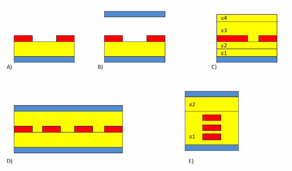
Examples of supported transmission line configurations. A) coupled microstrip B) coupled microstrip with a shield C) asymmetric coupled microstrip in inhomogeneous dielectric D) edge-coupled 4-conductor stripline E) broad-side coupled line in inhomogeneous dielectric
Related Topics
- Benefits of rfTlineLib
- Comparison of rfTlineLib and analogLib Mtline
- Location of rfTlineLib
- Structure of the rfTlineLib Library
- An Example of rfTlineLib
- Using rfTlineLib
- rfTLineLib Cells
- Microstrip Components
- Stripline Components
- Obsolete Components
Benefits of rfTlineLib
The rfTlineLib transmission line models offer the following benefits:
-
Accuracy:
rfTlineLibtransmission line models, such as mlin and slin, are based on rigorous EM simulations and include state-of-the-art descriptions of dielectric and conductor losses. Their applicability extends to long transmission lines and wide frequency ranges. The models have been tested extensively against standard industry benchmarks and 3D EM models, matching them within 1% or better.
The runtime simulation performance of newrfTlineLibmodels is comparable to empirical transmission line models and low-order lumped approximations. The use of EM-based transmission line parameters means that, in general, the initial extraction takes considerably longer, a few seconds in typical cases. However, instance and cross-section based caching makes EM extraction a one-time cost. As a result, in typical use, the overall simulation performance remains highly efficient. -
Ease of Use: stackup, a new cell in
rfTlineLib, defines common substrate properties.stackupoffers several pre-configured and commonly used layer stacks and the ability to define custom substrates behind an easy to use, graphical editor. Transmission line cells reference the common substrate definition without the need to re-enter shared parameters. - Smart Discontinuities: rfTlineLib discontinuities - tees, bends, curves and others - do not require users to specify redundant connectivity information. Instead, the properties of adjacent lines are collected automatically from the circuit's topology.
Limitations
The rfTlineLib transmission line models have the following limitations:
- Discontinuity models are not supported in shooting envelope and shooting-based pss.
- Discontinuities are modeled as short-circuits in transient.
-
rfTlineLibdoes not support coplanar waveguide configurations.
Related Topics
- rfTlineLib Library
- Comparison of rfTlineLib and analogLib Mtline
- Comparison of rfTlineLib and analogLib Mtline
- Location of rfTlineLib
- Structure of the rfTlineLib Library
Comparison of rfTlineLib and analogLib Mtline
rfTlineLib transmission lines are based on Spectre mtline technology and are netlisted as instances of mtline. In that sense, rfTlineLib models may be viewed as features of mtline and not a substitute.
mtline has been enhanced significantly to support rfTlineLib. These enhancements include:
- Improvements to EM solver accuracy. The solver is now within 1% of the established benchmarks.
-
New Spectre primitives -- including stackup, dielectric, and conductor - and new
mtlineparameters, to support a common substrate definition and the ability to reference it from mtline. - New frequency-dependent models of dielectric losses, including Debye, Wideband Debye, and table-based models.
- The Hammerstad surface roughness model for enhanced modeling of conductor losses.
- EM solver speed improvements.
In most cases, users will find rfTlineLib models more intuitive and convenient than analogLib mtline. Nevertheless, there are several use scenarios in which analogLib mtline is the only choice. They include coplanar waveguide configurations and the use of RLGC-form input as transmission line parameters.
Related Topics
- rfTlineLib Library
- Benefits of rfTlineLib
- Comparison of rfTlineLib and analogLib Mtline
- Location of rfTlineLib
- Structure of the rfTlineLib Library
Location of rfTlineLib
In MMSIM 12.1.1 and IC 6.1.6 ISR1 or newer versions, rfTlineLib is located in the following directory:
$(compute:THIS_TOOL_INST_ROOT)/tools/dfII/samples/artist/rfTlineLib
To use this library, specify the following in your cds.lib file or include it in the library path editor:
DEFINE rfTlineLib $(compute:THIS_TOOL_INST_ROOT)/tools/dfII/samples/artist/rfTlineLib
Related Topics
- rfTlineLib Library
- Benefits of rfTlineLib
- Comparison of rfTlineLib and analogLib Mtline
- Structure of the rfTlineLib Library
Structure of the rfTlineLib Library
rfTlineLib is organized in the following two categories for easier access and browsing:
TransmissionLines
This category contains the following new transmission line cells:
- maclin: asymmetric 2-conductor coupled microstrip
- mclin: coupled 2-conductor microstrip
- mlin: single-conductor microstrip
- coplanar: coplanar waveguide
- sclin: coupled 2-conductor stripline
- slin: single-conductor stripline
- nclin: n-conductor transmission line
Behavioral
Obsolete
Legacy models including microbend2, microbend90, microopenend, microstep, microstrip, stripbend90, and stripline have been moved to category Obsolete and remain supported for backward compatibility but are otherwise not recommended.
Discontinuities
The following cells have been discontinued:
- mtee: microstrip T-junction
- mbend: mitered arbitrary angle microstrip bend
- mbend2: mitered 90 degree microstrip bend
- mcorn: microstrip corner
- mcros: microstrip cross
- mstep: microstrip step
- stee: stripline T-junction
- sbend: mitered, arbitrary angle stripline bend
- sbend2: mitered 90 degree stripline bend
- scros: stripline cross
- sstep: stripline step
- mcurve: microstrip curve
- scurve: stripline curve
- mloceff: micsrostrip open-circuit effect
-
sloceff: stripline open-circuit effect
Related Topics
- rfTlineLib Library
- An Example of rfTlineLib
- Obsolete Components
- Microstrip Components
- Stripline Components
An Example of rfTlineLib
The following example illustrates the features of rfTlineLib.
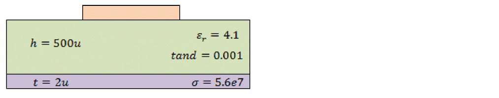
Consider a microstrip trace on 500u FR4, with 2u copper traces and ground plane, as shown below.
Step 1: Insert a stackup object
To define this stack, begin by placing a stackup instance on the schematic, as shown below.
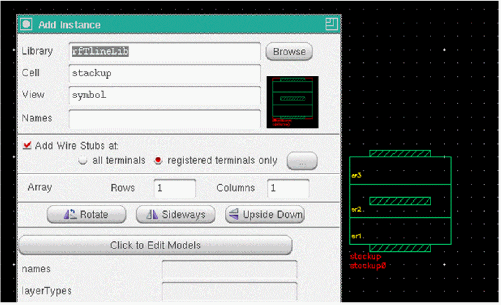
Transmission lines will reference the stackup (shown later). Any number of stackup objects may be present, although in practice, one is usually sufficient. Stackups may be placed anywhere in the hierarchy.
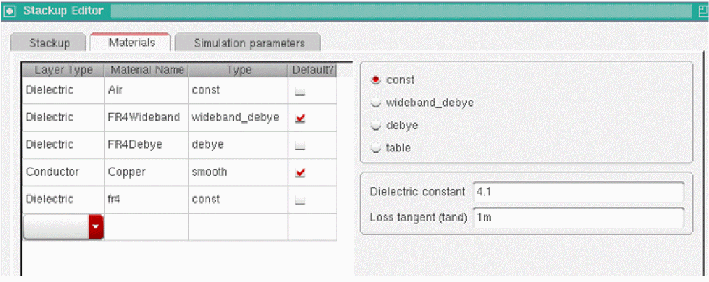
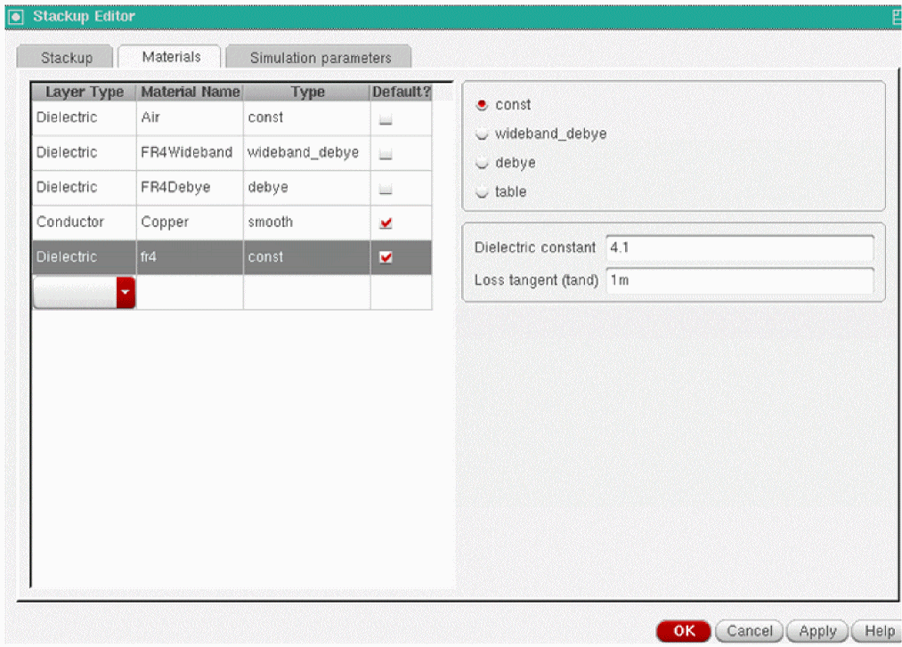
Step 2: Define material properties
Click the button labeled Click to Edit Models on the Add Instance form to edit the stack, and click the Materials tab. This is where you set the material properties of conductors and dielectrics.
Select a new dielectric from the drop-down list, as shown below.
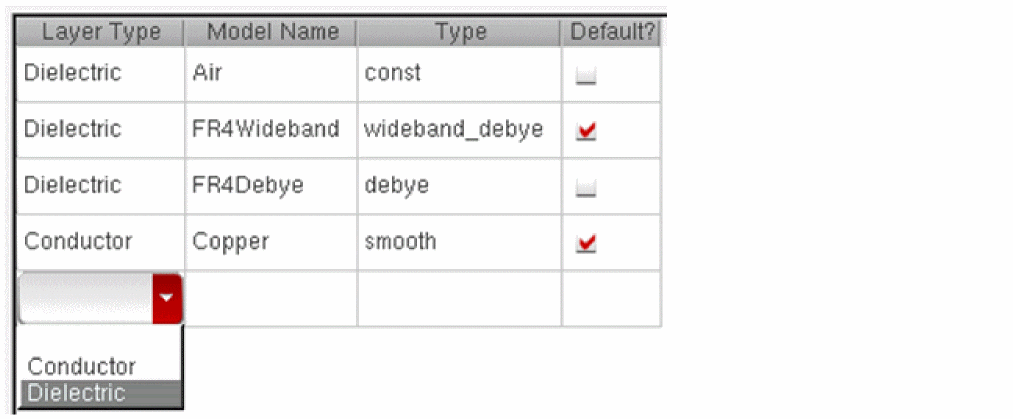
Name the material fr4, choose the constant loss model, and let the relative permittivity and loss tangent equal 4.1 and 0.001, respectively. The material database should look as follows:
Step 2.1: Setting default materials
If you want fr4 to be the default material when adding new dielectric layers to the stack, select the check box in the Default column for fr4, as shown below:
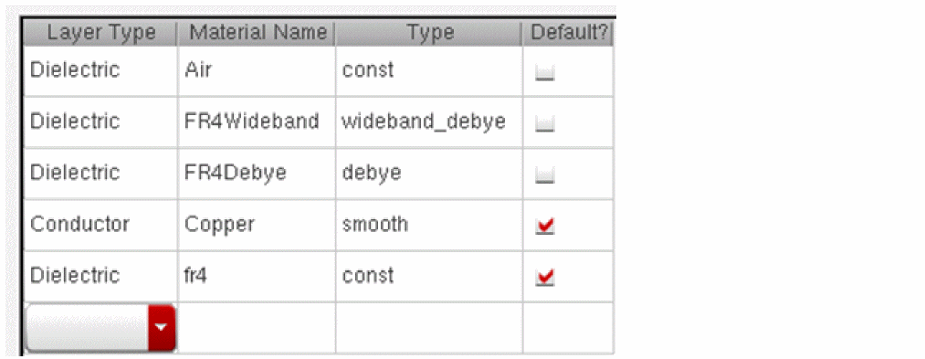
Now, newly added conductors will use Copper, and dielectrics will use fr4 by default.
Step 3: Define the layer stack
Next, click the Stackup tab to define the layer stack. In our case, we can choose the Microstrip configuration, the Microstrip/Stripline configuration, or we can enter our own configuration from scratch. In this step, we will define our own configuration to illustrate the process of defining a layer stack.
Select Modified from the Choose Configuration drop-down list, and enter three layers as follows:
- Click Add reference, name it ground, set the thickness to 2 microns (2e-6 or 2u), and make sure that it uses Copper as the model.
- Click Add dielectric, leave the name at default, and set the thickness to 500u. Select fr4 by double-clicking on the Material cell and choosing fr4.
- Click Add top/bottom microstrip, set the name to signalTop, let the thickness be 2u, and make sure that the Material cell specifies Copper.
The layer stack should now look as follows:
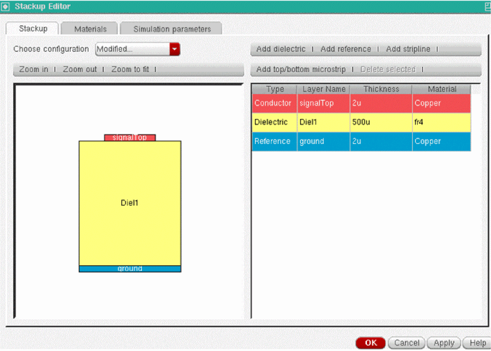
Click OK and then OK again to exit the CDF form. The stackup is now ready for use.
Step 4: Insert a transmission line
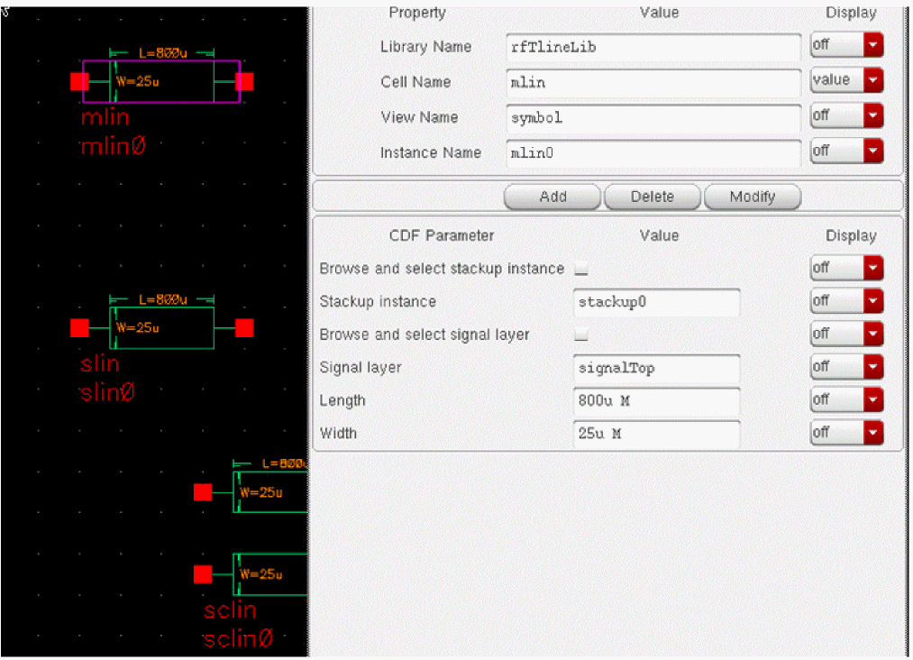
Insert a stackup0 in our case) and the layer name of the microstrip signal conductor (signalTop in our case). Ground layers are identified automatically and are not parameters of transmission line cells. Note the existence of layer and signal name browsers on the CDF form. If the stackup object is placed on the same schematic as the lines, you can use the browsers for easy specification of layer and stackup names. Clicking Browse and selecting stackup instance displays the names of the stackup instances on the schematic. Similarly, for a given stackup instance, browsing and selecting signal layer lists all its signal conductors.
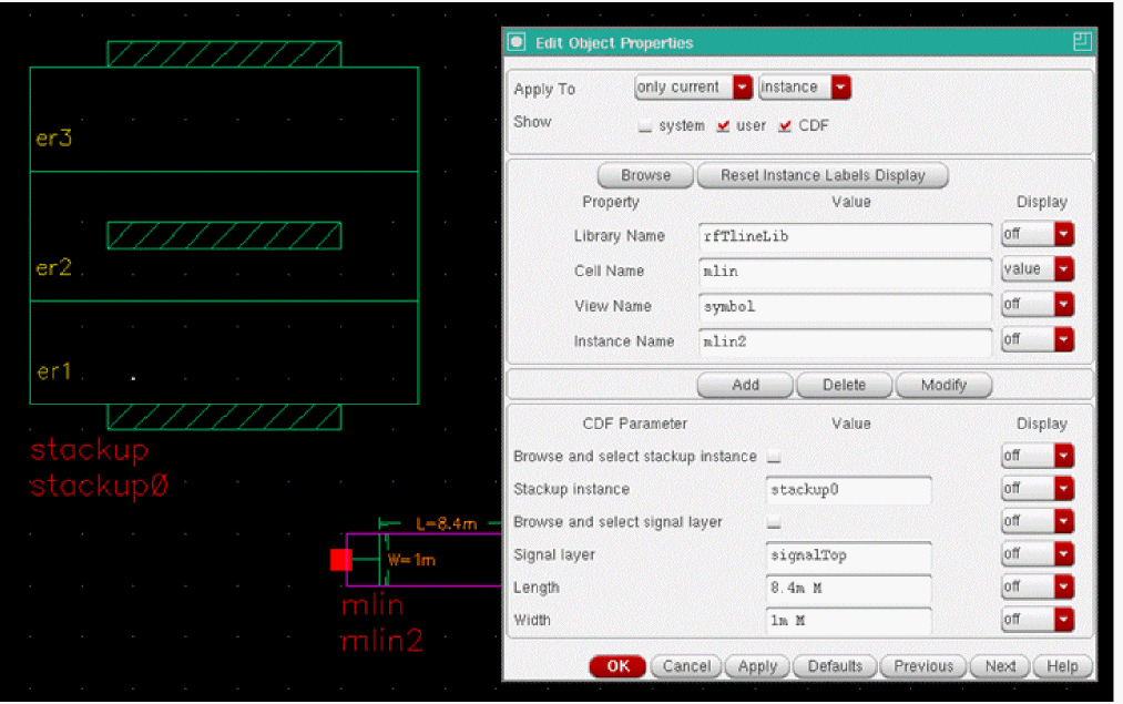
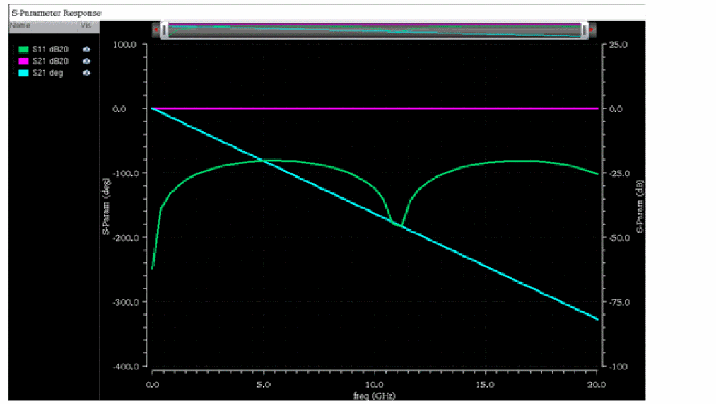
Let the width and length be equal to 1 millimeter (1m) and 8.4m, respectively. The microstrip line is ready to be used in the simulation. Simulate 50-Ohm S-parameters from DC from 20 GHz to obtain the following response:
Related Topics
- rfTlineLib Library
- Benefits of rfTlineLib
- Comparison of rfTlineLib and analogLib Mtline
- Structure of the rfTlineLib Library
- Using rfTlineLib
Using rfTlineLib
The Stackup
rfTlineLib transmission line cells reference stackup objects. Stackup objects store material properties and cross section information. Stackups may be placed anywhere in the hierarchy and are specified by their Spectre-style hierarchical paths.
Dielectric Models
rfTlineLib offers four methods of modeling frequency dependence of relative permittivity ![]() :
:
-
Constant
 and loss tangent (tan
  )
) - Wideband Debye model as proposed by Djordjevic-Sarkar [Ref. 1] and Svensson-Dermer [Ref. 2]
- Multipole Debye model
- Table model that constructs the multipole Debye model from the specified table of frequency-dependent dielectric constant and tangent delta
Constant Model
The constant model assumes no frequency dependence. In particular, the relative permittivity ![]() is of the form:
is of the form:

You specify the constant model by setting the dielectric constant ![]() and the loss tangent tan
and the loss tangent tan![]() in the stackup object, as shown below.
in the stackup object, as shown below.
The constant model is the oldest and most commonly used in the frequency domain. A drawback of this model is that it is non-causal if tan![]() . In practical use, the constant dielectric model is recommended for dielectrics with very low loss, such as Duroid, Silicon dioxide (SiO2), and so on. The largest loss tangent that should be used in this entry is 0.005. Since many commercial EM simulators implement the constant dielectric model, it may also be useful for comparison and verification.
. In practical use, the constant dielectric model is recommended for dielectrics with very low loss, such as Duroid, Silicon dioxide (SiO2), and so on. The largest loss tangent that should be used in this entry is 0.005. Since many commercial EM simulators implement the constant dielectric model, it may also be useful for comparison and verification.
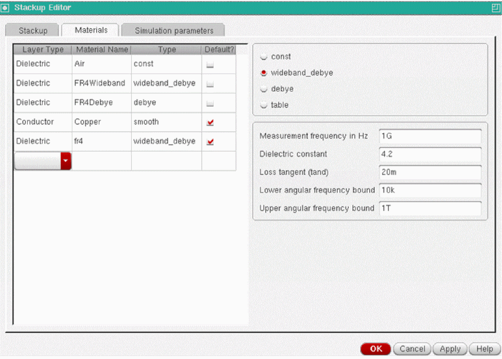
Wideband Debye
The Wideband Debye model expands the relative permittivity as [Ref. 1, 2].

The model is constructed from the following user-specified data:
- The measurement frequency
- The dielectric constant and the loss tangent at the measurement frequency
-
 1and
1and  2, angular frequency bounds, whose typical values are 1-1e4 rad/s and 1e10 to 1e12 rad/s, respectively;
Wideband Debye is a causal model for frequency-dependent dielectric constant of lossy dielectrics. It is constructed from the values of the dielectric constant and the loss tangent at one frequency point, so it combines the simplicity of the constant model with the benefit of causal response. The other two parameters ( ![]() 1and
1and ![]() 2 ) are the lower and upper bound of the angular frequency where the loss tangent tan
2 ) are the lower and upper bound of the angular frequency where the loss tangent tan![]() varies approximately linearly with frequency. The model is not very sensitive to these values, so setting
varies approximately linearly with frequency. The model is not very sensitive to these values, so setting ![]() 1=100 and
1=100 and ![]() 2=1e12 is reasonable. This model is most commonly used for the FR-4 dielectric and pre-preg utilized to manufacture common PCBs. It is recommended for the modeling of FR-4 PCBs.
2=1e12 is reasonable. This model is most commonly used for the FR-4 dielectric and pre-preg utilized to manufacture common PCBs. It is recommended for the modeling of FR-4 PCBs.
The model is constructed such that the frequency-dependent dielectric constant and tangent delta of the model matches those given at the measurement frequency, and the loss tangent varies approximately linearly between ![]() 1and
1and ![]() 2. Note that in Spectre the angular frequencies are specified,
2. Note that in Spectre the angular frequencies are specified, ![]() 1=2
1=2![]() f1 and
f1 and ![]() 2=2
2=2![]() f2.
f2.
You specify the Wideband Debye model parameters in the Stackup Editor, as follows:
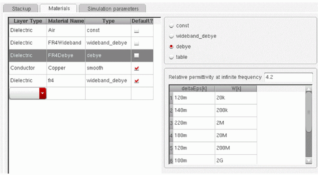
Debye
The Debye model uses the following multi-pole expansion:
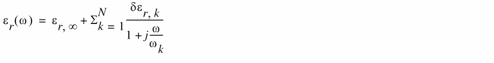
N, ![]() ,
, ![]() k and
k and ![]() are model parameters and are specified by the user and entered in
are model parameters and are specified by the user and entered in
the Stackup Editor, as shown below.
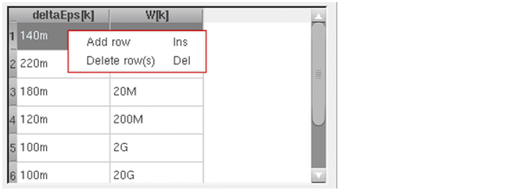
To add or delete a row of data, select the row, right-click, and select Add row or Delete row(s) from the context menu. Alternatively, use the bindkeys, as shown below.
Multipole Debye is recommended for the dielectrics for which the Wideband Debye model does not describe the frequency dependence well. It can approximate the experimental data of the frequency dependent dielectric constant more closely than the wideband Debye model provided the experimental results are available at a sufficient number of frequency points. Note that it is necessary to have at least three frequency points to construct a usable multipole Debye model, and it is recommended to have at least 10 frequency points [Ref. 3].
We preload the published multipole Debye model for FR-4 from Djordjevic-Sarkar's paper [1].
Table Model
The table model assumes a general frequency-dependence of the relative permittivity.
You can specify ![]() and
and ![]() in tabular format, as shown below.
in tabular format, as shown below.
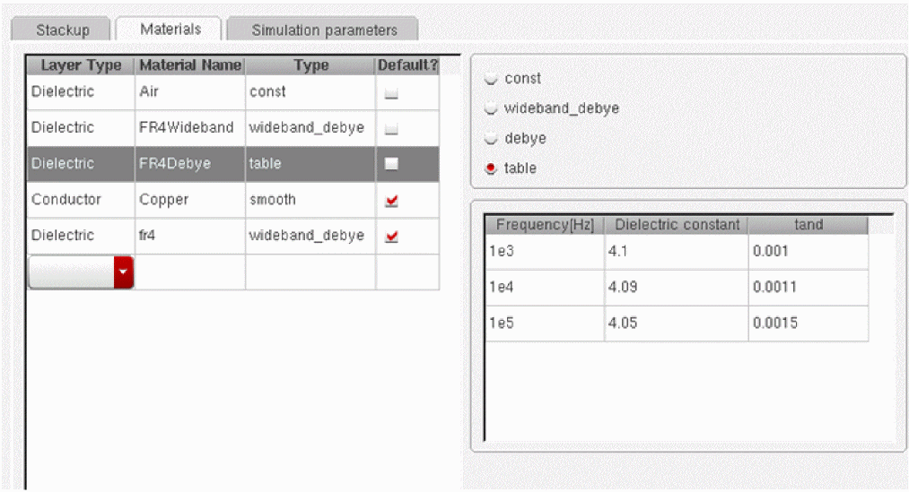
You can add and delete rows by selecting a row and right-clicking or by using Insert and Delete bindkeys, similar to the Debye model.
Adding Dielectric Material Models
The material browser is pre-configured with several default materials. You can add as many materials as you wish by using the drop-down menu at the bottom of the model table:
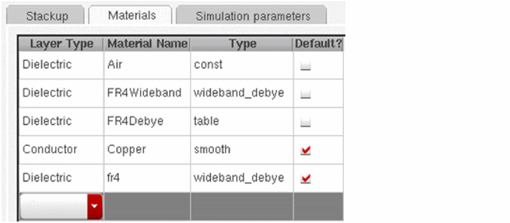
To change the name of a material, double-click the Material Name cell. Default materials are those that are assigned automatically to the newly added layers. A material is designated as a default material by selecting the Default? check box.
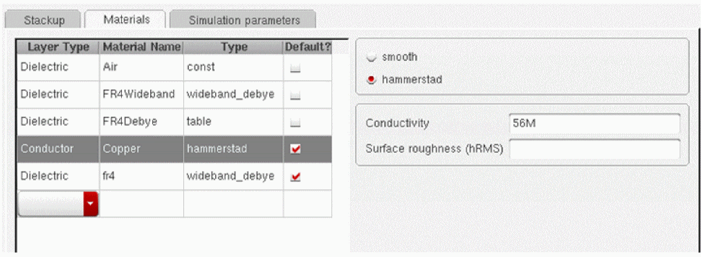
Conductors
Conductors are specified in terms of their conductivity ![]() in S/m. One can model smooth conductor surfaces (smooth), or model the surface roughness included by means of Hammerstad formula [4] (hammerstad).
in S/m. One can model smooth conductor surfaces (smooth), or model the surface roughness included by means of Hammerstad formula [4] (hammerstad).
The Hammerstad model introduces the RMS tooth height parameter hRMS (the units of length, typical value in micrometers), and accounts for the increase of the frequency dependent resistance and inductance per unit length through the use of the Hammerstad coefficient.

where ![]() is the skin-depth. The 2-D EM calculations are performed for the
is the skin-depth. The 2-D EM calculations are performed for the
conductors with the smooth surface, and the parameters of the transmission line with rough conductor surfaces, RH ![]() and LH
and LH ![]() are calculated from those for the smooth conductor surfaces, R
are calculated from those for the smooth conductor surfaces, R![]() and L
and L![]() according to the expressions below.
according to the expressions below.
This approach assumes that all conductors have the same roughness.
To specify the smooth model, enter the conductivity, as shown: below.
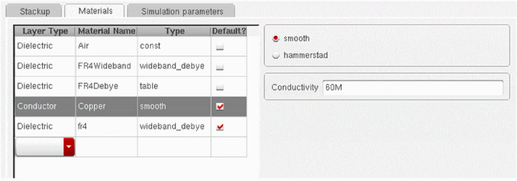
To include the roughness model, select hammerstad and specify the conductivity and RMS height, as shown below.
Adding Conductor Materials
You can add as many conductor materials as you wish. The procedure is similar to adding dielectrics.
Configuring Layers
Use the Stackup tab to set up your substrate. The Substrate Editor is preconfigured with three layer stacks: Microstrip/Stripline, Microstrip, and Stripline. The existing configurations are sufficient to describe many practical scenarios. The Microstrip/Stripline configuration is the most general of the three, and is shown below.
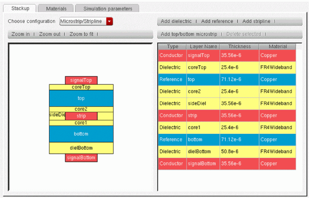
Since Microstrip/Stripline already includes two microstrip and one stripline configuration, the standalone Microstrip and Stripline are included mainly as examples. You can freely use the more general stack to define simpler cross-sections. Internally, the solver automatically strips away the unused layers. For example, if a microstrip line were defined on signalTop, the solver would ignore everything beneath the top ground plane. Similarly, if a stripline were defined on strip, everything above top and below bottom would be ignored without performance penalty.
To edit layer names, thicknesses or model types, double-click the appropriate cell and edit as appropriate.
Entering Custom Layer Stacks
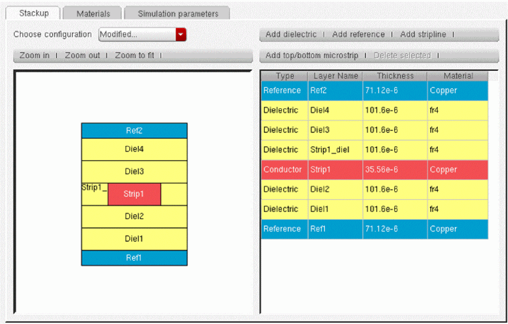
To enter an arbitrary stack, delete the existing configuration by selecting all layers (click on the top layer in the table or the graphical view, then <SHIFT>+click on the bottom layer, and choose Delete selected). Starting from the bottom, enter the appropriate layer one at a time by choosing the appropriate commands using the button strip in the top right corner. The following stack is produced by the sequence of commands: Add reference>Add dielectric>Add dielectric>Add stripline>Add dielectric>Add dielectric>Add reference.
Inserting Layers
Layers are inserted by selecting a layer and using one of the Add layer commands. New layers are always added on top of the selected stack. If no layer is selected, new layers are added to the top of the stack.
Bindkeys
The following bindkeys are supported:
- Zoom in: <Ctrl>+L
- Zoom out: <Ctrl>+S
- Zoom to fit: <Ctrl>+F
- Delete layers, models or rows in material model tables:<Delete>
- Add rows in material model tables: <Insert>
Units
Layer thicknesses are expressed in meters. The use of scale factors, such as p, n, u, m, K, M and G is supported. You can specify thickness in mils but the stack editor will automatically convert them to meters. For example, typing in "2mil" for the thickness of a layer will automatically convert it to 50.8u.
Adding Transmission Lines
Transmission lines reference stackup objects by means of the Stackup instance parameter, as shown below.
Stackup instance is a hierarchical instance path in the Spectre language format. Thus:
- stackup0 matches an instance defined at the current level of hierarchy or any of the parents, in that order of precedence.
- I0.stackup0 matches a stackup object defined in subcircuit instance I0 defined at the present level of hierarchy or at the top-level circuit, in that order of precedence.
Select the Browse and select stackup instance check box to display the stackup browser. Similarly, select the Browse and select signal layer check box to display a list of signal layers for the chosen stackup. The browsing aids work only when the stack is defined on the same schematic as the transmission line instance.
Working With Transmission Line Discontinuities
Transmission line discontinuities are in the category Discontinuities. Discontinuities have the following important properties:
Automatic Detection of Adjacent Lines
rfTlineLib discontinuities are aware of the lines that connect to them and do not require you to specify their geometric and material properties. This information is detected by Spectre at runtime and passed automatically.
Discontinuities Cannot be Simulated Unless They Connect to Transmission Lines
To be simulateable in Spectre, discontinuities must be connected to transmission lines. Leaving them open-circuited or connected to other device types results in Spectre simulation errors.
Discontinuities are Short Circuited in Transient Simulation
In transient and PSS shooting simulations, discontinuities are treated as short-circuits. This is a limitation of the present implementation that will be resolved in future releases.
rfTLineLib Cells
The rfTlineLib library contains the following cells:
MLIN
SYMBOL
Command-line help
CDF Parameters
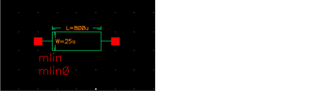
mlin is not limited to traditional microstrip configurations in the strictest sense of the word - with air above the conductor and a homogeneous dielectric beneath. In fact, the stackup can include any number of dielectric layers of arbitrary material properties, and an optional ground shield above the conductor.mlin is in effect a general single conductor line above ground (with an optional ground shield). The mlin cell was provided for convenience and for naming compatibility with legacy microwave EDA tools.
Similar comments apply to coupled microstrip cells like mclin and maclin.
Example
mlin0 (net1 net2 0 0) mtline stackup=stackup0 layer=["signalTop"] len=800u linewidth=[25u]
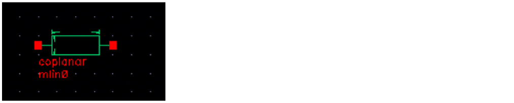
COPLANAR
SYMBOL
Command-line help
Structure
CDF Parameters
Example
Mline0 (net1 net2 0 0) mtline linetype=coplanar stackup=stackup0
+ Layer=[“signaltop” ] len=(800u) linewidth=[(25u) (25u) (25u) ]
+ linespace=[(25u) 25u) ]
SLIN
SYMBOL
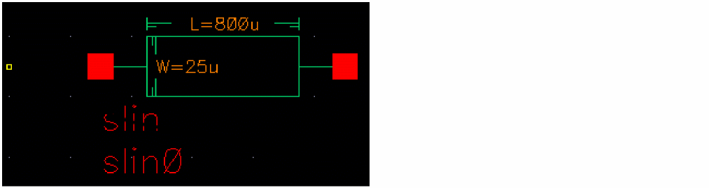
Command-line help
spectre -h mtline
CDF Parameters
The slin cell was provided for convenience and for naming compatibility with legacy microwave EDA tools but is more general than legacy implementations.
Similar comments apply to coupled stripline cells.
Example
slin0 (net1 net2 0 0) mtline stackup=stackup0 layer=["strip"] len=800u linewidth=[25u]
MCLIN
SYMBOL
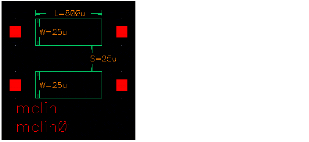
Command-line help
spectre -h mtline
CDF Parameters
Example
mclin0 (net1 net2 net3 net4 0 0) mtline stackup=stackup0 layer=["signalTop"] len=800u linewidth=[25u 25u] linespace=[25u]
MACLIN
SYMBOL
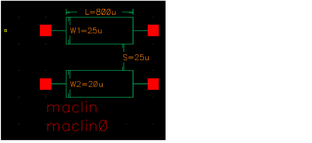
This cell is similar to mclin, but it allows you to specify lines of different width.
Command-line help
spectre -h mtline
CDF Parameters
maclin is in effect a general single conductor line above ground (with an optional ground shield). The mlin cell was provided for convenience and for naming compatibility with legacy microwave EDA tools.
Example
maclin0 (net1 net2 net3 net4 0 0) mtline stackup=stackup0 layer=["signalTop"] len=800u linewidth=[25u 25u] linespace=[25u]
SCLIN
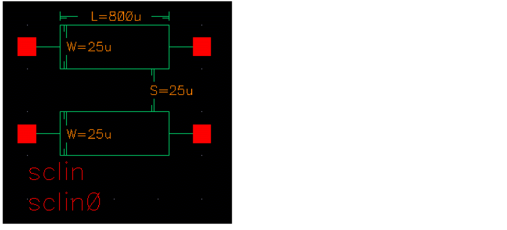
Coupled stripline
Command-line help
spectre -h mtline
CDF Parameters
The sclin cell was provided for convenience and for naming compatibility with legacy microwave EDA tools but is more general than legacy implementations.
Example
sclin0 (net1 net2 net3 net4 0 0) mtline stackup=stackup0 layer=["strip"] len=800u linewidth=[25u 25u] linespace=[25u]
SYMBOL: NCLIN
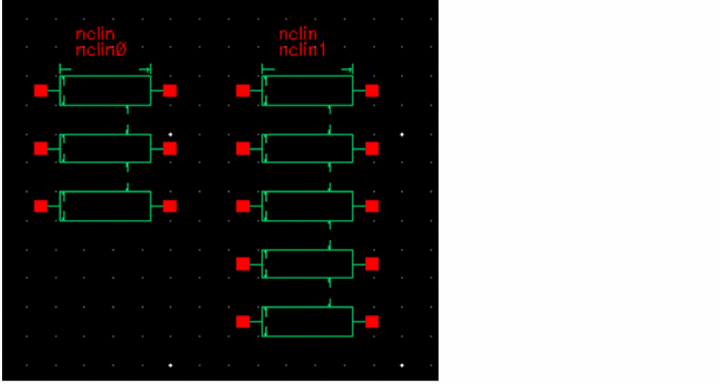
N coupled conductors
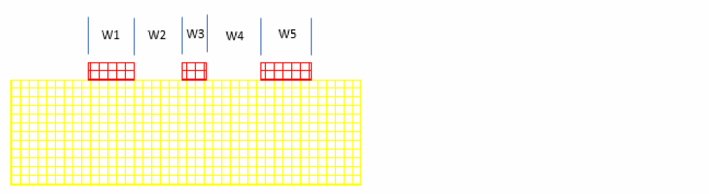
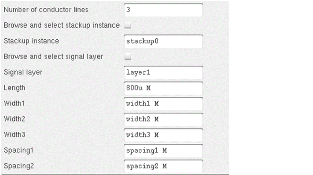
nclin is a parametric cell which lets you specify a transmission line consisting of N coupled conductors. N is between 1 and 64.
For an N conductor line, you specify N widths and N-1 spacings. In the CDF form, the widths and spacings are specified using parameters Width1, Width2, … WidthN and Spacing1, Spacing2,..... SpacingN-1. On the symbol, Width1 corresponds to the top line, and WidthN corresponds to the bottom line.
Line spacing is measured from edge-to-edge, as shown (cross-section view) below.
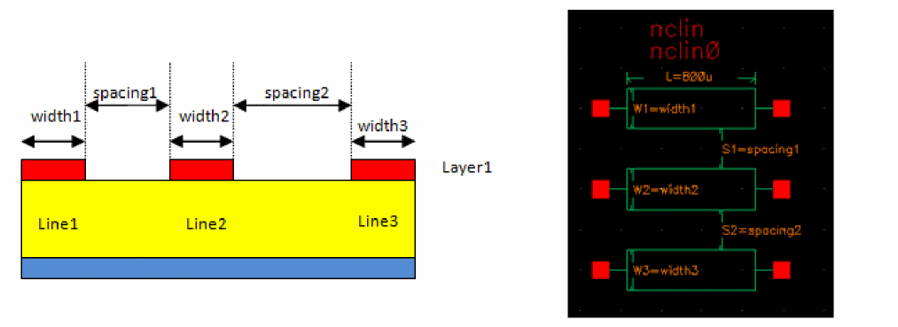
Assuming that a conductor by the name of Layer1 is defined in the stackup, the CDF form for the above configuration would look, as shown below.
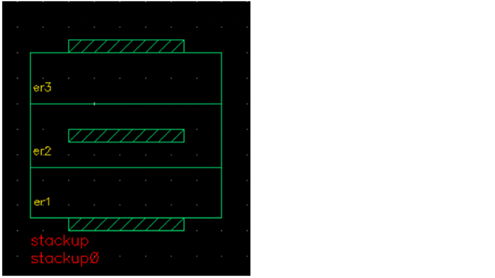
You can also define broad-side coupled lines (coupled lines on multiple layers). Consider the following example:
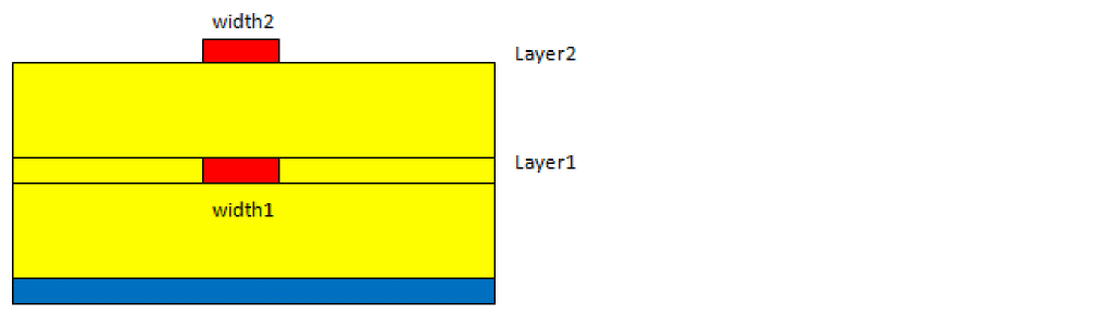
Since spacing is defined as starting from the right edge of one line to the left edge of the next, we use negative spacing to position them on top of one another. Therefore, the CDF form would look like the following:
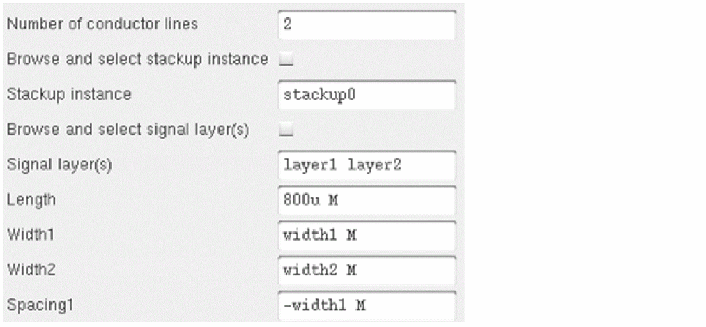
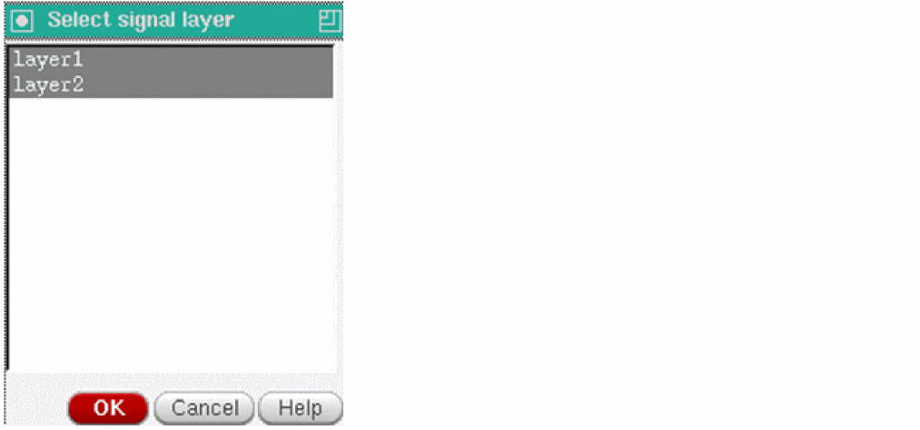
To specify more than one layer, you can type in a comma-separated list of names, as shown, or use <SHIFT>+click or <CTRL>+click key combinations to select multiple layer names in the Select signal layer browser.
Command-line help
spectre -h mtline
CDF Parameters
Example
nclin0 (net1 net2 net3 net4 0 0) mtline stackup=stackup0 layer=["strip"] len=800u linewidth=[25u 25u] linespace=[25u]
SYMBOL: STACKUP
Stackup
This cell is used to define common geometric and material properties of transmission lines. The netlisting of the stackup cell includes several Spectre devices, such as stackup, dielectric, and conductor.
Command-line help
spectre -h stackup
spectre -h dielectric
spectre -h conductor
CDF Parameters
Example
stackup0 stackup names=["signalBottom" "dielBottom" "bottom" "core1" "strip" "sideDiel" "core2" "top" "coreTop" "signalTop" ] type=["Cond" "Diel" "Ref" "Diel" "Cond" "Diel" "Diel" "Ref" "Diel" "Cond" ] thickness=[35.56u 50.8u 71.12u 25.4u 35.56u 35.56u 25.4u 71.12u 25.4u 35.56u] material=[Copper FR4 Copper FR4 Copper FR4 FR4 Copper FR4 Copper]
FR4 dielectric type="wideband_debye" nd=5 data=[1G 4.2 20m 10K 1T]
Copper conductor type="smooth" nd=1 data=[56M]
SYMBOL: MTEE
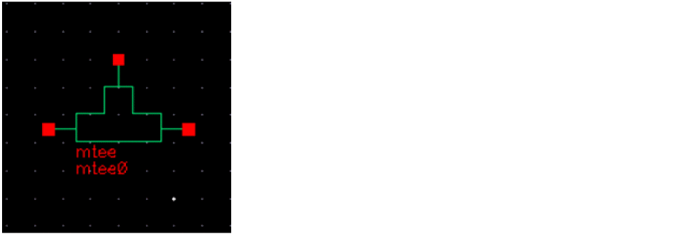
Microstrip tee junction
A tee instance must have exactly three transmission line instances connecting to its terminals, one transmission line per terminal. All three transmission lines should refer to the same stackup. It is an error to have instances of any other model connect to the terminals of a tee.
The geometric and material information is obtained automatically from the transmission line instances.
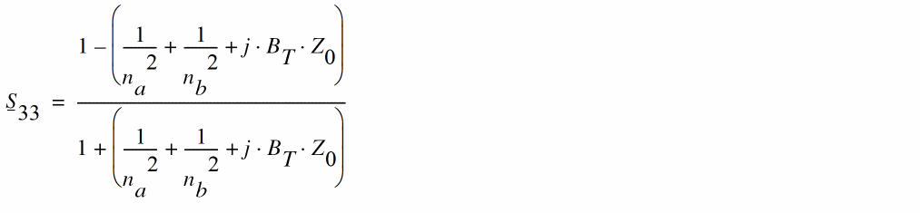
A diagram of the physical microstrip tee junction and the equivalent circuit is shown below.
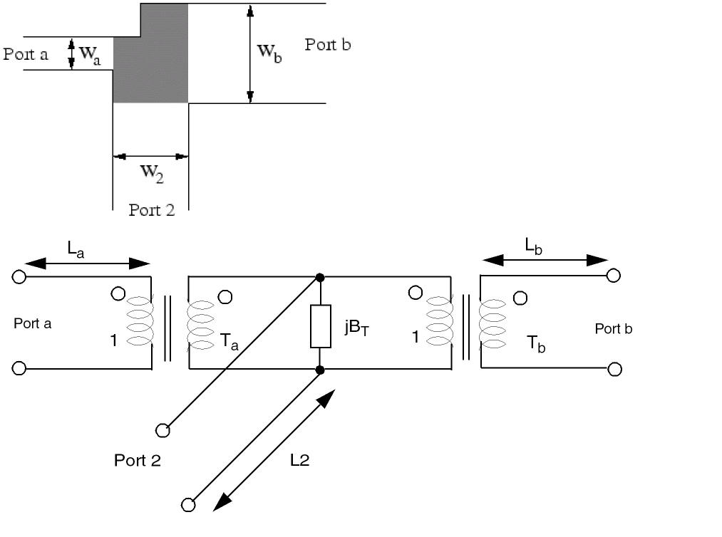
A model of the microstrip tee junction shows a unsymmetrical microstrip tee with the main arms consisting of port a and b and with the side arm consisting of port 2. The grayed portion marks the area modeled by the equivalent circuit (shown at the bottom). The equivalent circuit consists of a shunt reactance BT, one transformer in each main arm (ratios Ta and Tb) and a microstrip line in each arm (width Wa, Wb, and W2).
The equivalent parallel plate line width is given by:
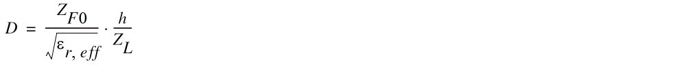
ZF0 is the vacuum field impedance, h is the height of substrate, ![]() is the effective,relative dielectric constant, and ZL is the microstrip line impedance.
is the effective,relative dielectric constant, and ZL is the microstrip line impedance.
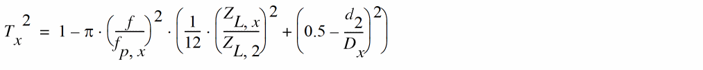
The first higher order mode cut-off frequency is given by:

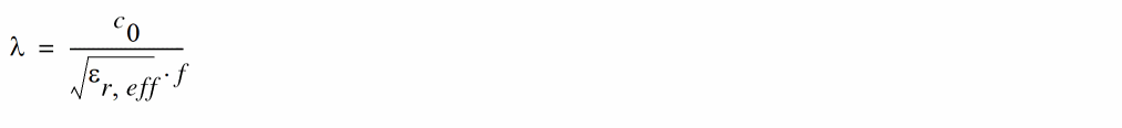
The effective wave length of the microstrip quasi-TEM mode is given by:

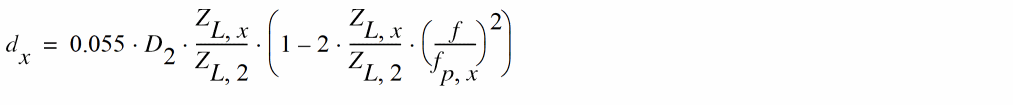
The main arm displacements of the reference planes from the center lines are (index x stand for a or b) given by:

The length of the line in the main arms is given by:
The side arm displacement of the reference planes from the center lines is given by:
The length of the line in the side arm is given by:
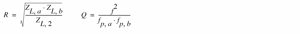
where max (x,y) is the larger of both the quantities.

The turn ratio of the transformers in the side arms is given by:

The shunt susceptance is given by:

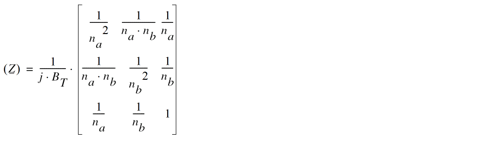
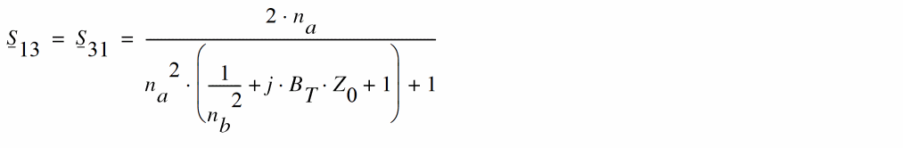
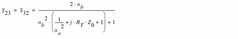
For better implementation of the microstrip tee, the device parameter of the internal equivalent circuit (two transformers and the shunt susceptance) are given below. The port numbering for them is port a = 1, port b = 2, and port 2 = 3.

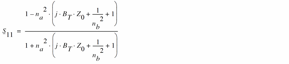
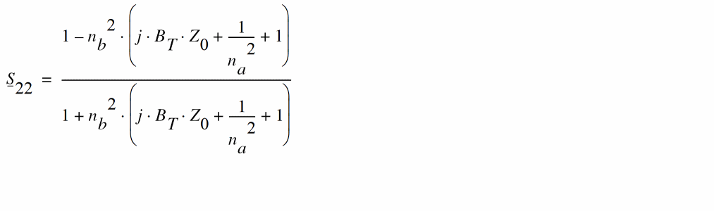


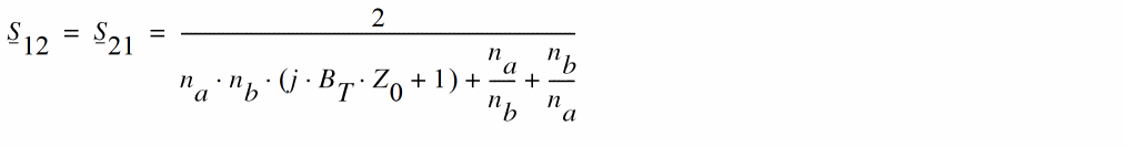
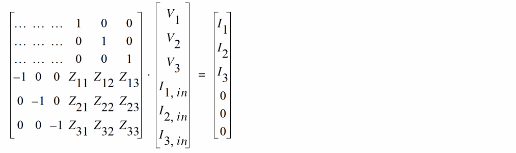
The MNA matrix representation can be derived from the Z parameters in the following way:

Note that the main arm displacements yield two small microstrip lines at each main arm and the side arm displacement results in a small microstrip strip line as well, but with negative length, that is a kind of phase shifter here.
The transformer ratios are negative with increasing frequency which produces complex values in the Z-parameter matrix as well as in the S-parameter matrix. That is why the ratios are delimited to a minimum value.
Spectre uses an augmented version of the Hammerstad model by accounting for the frequency-dependent characteristic impedance and the effective dielectric constant of the connecting transmission lines.
Command-line help
spectre -h tee
CDF Parameters
Range of Usage
The T-junction model is valid for the frequency range not exceeding the first high order mode cutoff frequency. The first high order model cutoff frequency, fp, can be calculated using
fp [GHz]= Zo/h[mm], where Zo is the characteristic impedance of the trace, and h is the substrate thickness. The results of the model for frequencies above the fp are not correct. The model achieves the best accuracy when the ratio of the trace width Wi to the substrate thickness h satisfies the inequality 1<=Wi/h <=10. The dielectric constant of the substrate should not exceed 12.8.
Example
mtee0 (net1 net2 net3) tee
SYMBOL: STEE
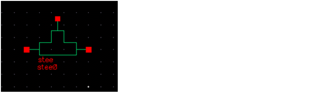
Stripline tee junction
A tee instance must have exactly three transmission line instances connecting to its terminals, one transmission line per terminal. All three transmission lines should refer to the same stackup. It is an error to have instances of any other model connect to the terminals of a tee.
The geometric and material information is obtained automatically from the transmission line instances.
A diagram of the physical microstrip tee junction and the equivalent circuit is shown below.

A model of the microstrip tee junction shows a unsymmetrical microstrip tee with the main arms consisting of port a and b and with the side arm consisting of port 2. The grayed portion marks the area modeled by the equivalent circuit (shown at the bottom). The equivalent circuit consists of a shunt reactance BT, one transformer in each main arm (ratios Ta and Tb) and a microstrip line in each arm (width Wa, Wb, and W2).
The equivalent parallel plate line width is given by:

ZF0 is the vacuum field impedance, h is the height of substrate, ![]() is the effective, relative dielectric constant, and ZL is the microstrip line impedance.
is the effective, relative dielectric constant, and ZL is the microstrip line impedance.
The first higher order mode cut-off frequency is given by:

The effective wave length of the microstrip quasi-TEM mode is given by:
The main arm displacements of the reference planes from the center lines are (index x stand for a or b) given by:
The length of the line in the main arms is given by:
The side arm displacement of the reference planes from the center lines is given by:
The length of the line in the side arm is given by:
where max (x,y) is the larger of both the quantities.
The turn ratio of the transformers in the side arms is given by:
The shunt susceptance is given by:

For better implementation of the microstrip tee, the device parameter of the internal equivalent circuit (two transformers and the shunt susceptance) are given below. The port numbering for them is port a = 1, port b = 2, and port 2 = 3.


The MNA matrix representation can be derived from the Z parameters in the following way:
Note that the main arm displacements yield two small microstrip lines at each main arm and the side arm displacement results in a small microstrip strip line as well, but with negative length, that is a kind of phase shifter here.
The transformer ratios are negative with increasing frequency which produces complex values in the Z-parameter matrix as well as in the S-parameter matrix. That is why the ratios are delimited to a minimum value.
Spectre uses an augmented version of this model by accounting for the frequency-dependent characteristic impedance and the effective dielectric constant of the connecting transmission lines.
Command-line help
spectre -h tee
CDF Parameters
Range of Usage
The model achieves the best accuracy for W1=W2, where W1 and W2 are the trace with for the traces connecting to the "top of the T". In case of ![]() , the geometric mean
, the geometric mean sqrt(W1*W2) is used which works for the trace width mismatch of up to 10%.
Denote the characteristic impedances of the transmission lines of the width W1 and W2 (connecting to the "top of the T") as Zo1 and that of the width W3 as Zo3. The condition 0.2 <=Zo1/Zo3 <=2 is required for the maximum accuracy. The stripline T-junction model is accurate for the frequency range up to the first high-order cut-off frequency.
Example
stee0 (net1 net2 net3) tee
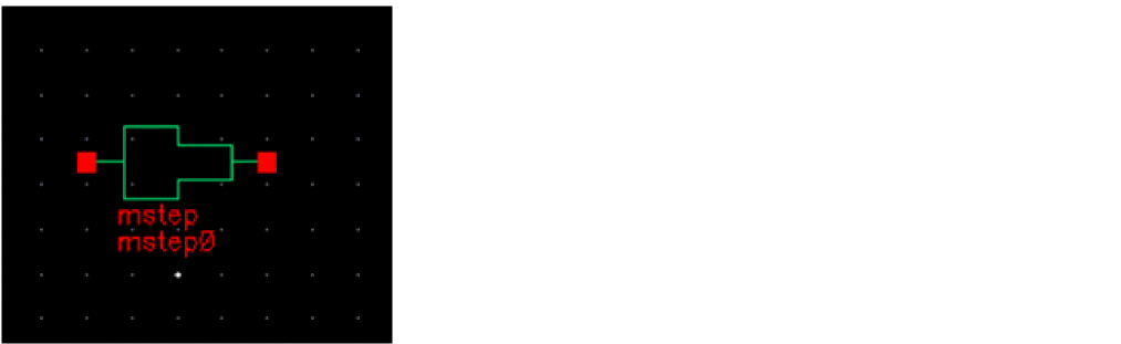
SYMBOL: MSTEP
Microstrip step in width (centered)
A step instance must have exactly two transmission line instances connecting to its terminals, one transmission line per terminal. Both transmission lines should refer to the same stackup. It is an error to have instances of any other model connect to the terminals of a step.
The geometric and material information is obtained automatically from the transmission line instances. The step junction model is based on the approximate full-wave EM analysis that involves transforming to an equivalent parallel plate waveguide and the use of mode matching technique, as described in:
T.S. Chu, T. Itoh, and Y.C. Shih 'Comparative Study of Mode-Matching Formulations for Microstrip Discontinuity Problems', IEEE Trans. MTT, V. 33, N. 10, 1985,and references within.
The advantage of this approach over the closed-form empirical formulas is its validity for a wide range of the dielectric constants.
Command-line help
spectre -h step
CDF Parameters
Range of Usage
The model is valid for the relative dielectric constant ranging from 1 to 12.8 (even though there is no hard upper limit), and the ratio of the trace width from 1 (for which the model acts as a short) to 20.
Example
mstep0 (net1 net2) step
SYMBOL: SSTEP
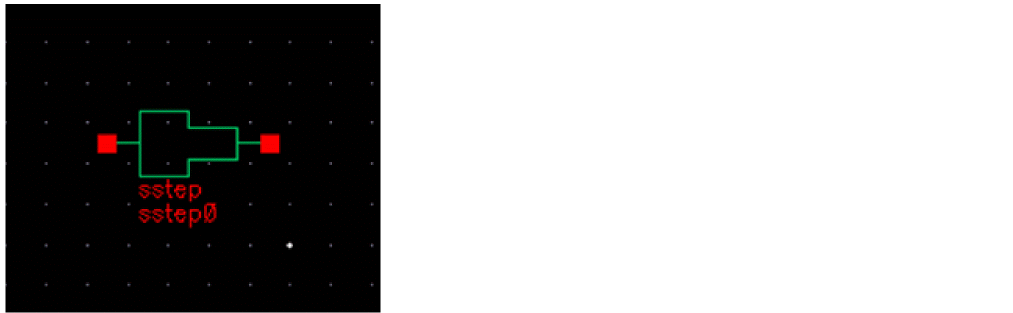
Stripline step in width (centered)
A step instance must have exactly two transmission line instances connecting to its terminals, one transmission line per terminal. Both transmission lines should refer to the same stackup. It is an error to have instances of any other model connect to the terminals of a step.
The geometric and material information is obtained automatically from the transmission line instances. The step junction model is based on the approximate full-wave EM analysis that involves transforming to an equivalent parallel plate waveguide and the use of mode matching technique, as described in:
T.S. Chu, T. Itoh, and Y.C. Shih 'Comparative Study of Mode-Matching Formulations for Microstrip Discontinuity Problems', IEEE Trans. MTT, V. 33, N. 10, 1985, and references within.
The advantage of this approach over the closed-form empirical formulas is its validity for a wide range of the dielectric constants.
Command-line help
spectre -h step
CDF Parameters
Range of Usage
The model is valid for the relative dielectric constant ranging from 1 to 12.8 (even though there is no hard upper limit), and the ratio of the trace width from 1 (in which case the model acts as a short) to 20.
Example
sstep0 (net1 net2) step
SYMBOL: MBEND2
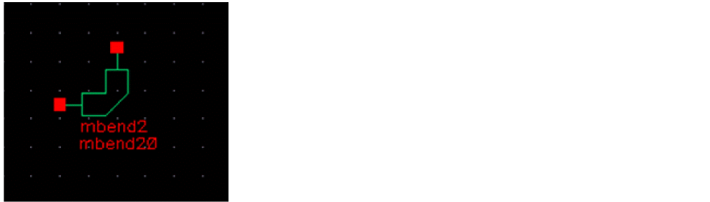
Microstrip optimally mitered 90 degree bend
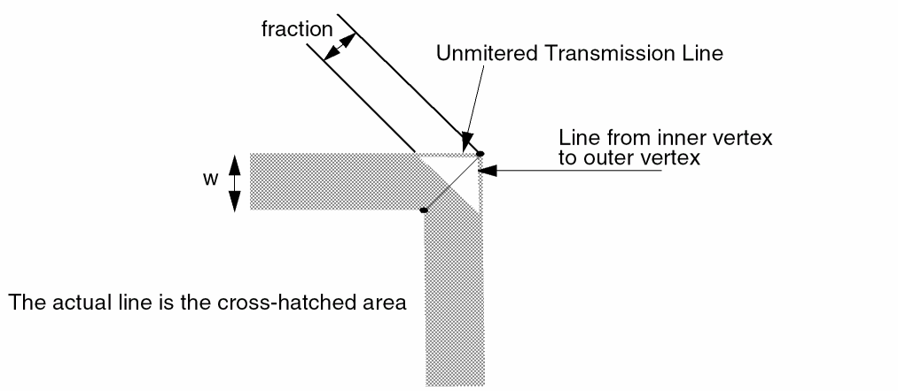
The geometry of the MBEND2 model is defined in the figure below. Both traces have the same width, W. The miter fraction M is defined as M=fraction/Line from inner to outer vertex, where fraction and line from inner to outer vertex are defined below.

The optimal miter fraction was determined experimentally [R. J. P. Douville and D. S. James, Experimental study of symmetric microstrip bends and their compensation; IEEE Trans. Microwave Theory Tech., vol. MTT-26, pp. 175-182, Mar. 1978] to be well approximated as M=(0.52+0.65exp[-1.35w/h]).
A bend2 instance must have exactly two transmission line instances connecting to its terminals, one transmission line per terminal. Both transmission lines should refer to the same stackup. It is an error to have instances of any other model connect to the terminals of a step.
The geometric and material information is obtained automatically from the transmission line instances.
The frequency-domain model is an empirically based model, which consists of a lumped equivalent circuit (T-network of two inductors and a shunt capacitor to ground). The equivalent circuit parameters are frequency-independent and are expressed as functions of trace width, dielectric height, and dielectric constant.
The expressions were developed by Kirschning, Jansen, and Koster and given in the following publication:
M. Kirschning, R. H. Jansen, and N. H. L. Koster. 'Measurement and Computer-Aided Modeling of Microstrip Discontinuities by an Improved Resonator Method', 1983 IEEE MTT-S International Microwave Symposium Digest, May 1983, pp. 495-497.
Command-line help
spectre -h mbend2
CDF Parameters
Range of Usage
The ratio of the trace width W to the substrate thickness h should satisfy 0.2<= W/h<=6.0. For the best accuracy, the dielectric constant Er should satisfy
The simulation frequency f should satisfy f[GHz]<12/h[mm].
Example
mbend20 (net1 net2) bend2
SYMBOL: SBEND2
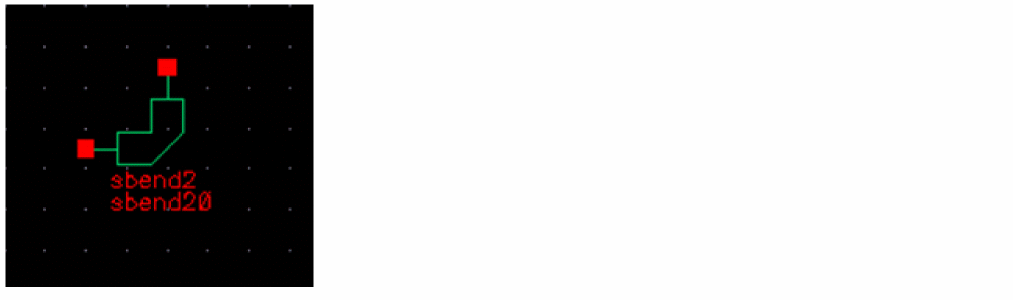
Stripline optimally mitered 90 degree bend
The geometry of the MBEND2 model is defined in the figure below. Both traces have the same width, W. The miter fraction M is defined as M=fraction/Line from inner to outer vertex, where fraction and the line are defined below.
A bend2 instance must have exactly two transmission line instances connecting to its terminals, one transmission line per terminal. Both transmission lines should refer to the same stackup. It is an error to have instances of any other model connect to the terminals of a step.
The geometric and material information is obtained automatically from the transmission line instances.
The frequency-domain model is an empirically based model which consists of a lumped equivalent circuit (T-network of two inductors and a shunt capacitor to ground). The equivalent circuit parameters are frequency-independent and are expressed as functions of trace width, dielectric height, and dielectric constant.
The expressions were developed by Kirschning, Jansen, and Koster and given in the following publication:
M. Kirschning, R. H. Jansen, and N. H. L. Koster. 'Measurement and Computer-Aided Modeling of Microstrip Discontinuities by an Improved Resonator Method', 1983 IEEE MTT-S International Microwave Symposium Digest, May 1983, pp. 495-497.
Command-line help
spectre -h bend2
CDF Parameters
Range of Usage
The ratio of the trace width W to the total dielectric thickness B should satisfy
Example
sbend20 (net1 net2) sbend2
SYMBOL: MBEND
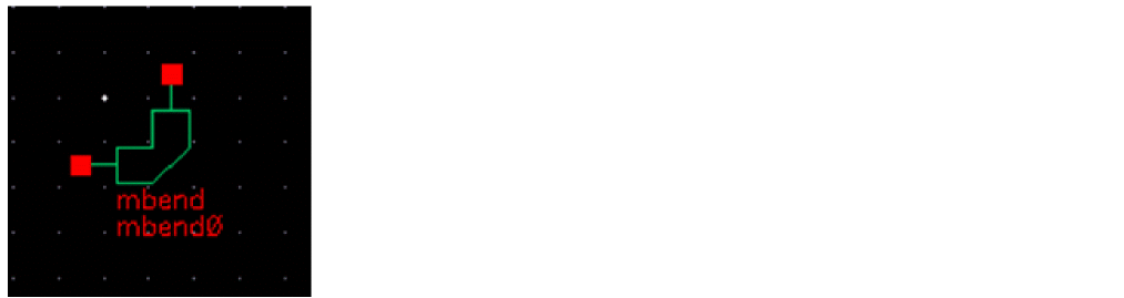
Microstrip bend with the specified angle and miter fraction
A bend instance must have exactly two transmission line instances connecting to its terminals, one transmission line per terminal. Both transmission lines should refer to the same stackup. It is an error to have instances of any other model connect to the terminals of a step.
The geometric and material information is obtained automatically from the transmission line instances.
The frequency-domain model is an empirically based model, which consists of a T-network of three impedances with two cascaded sections of transmission lines.
Command-line help
spectre -h bend
CDF Parameters
The miter angle is half the angle of the bend.
The miter fraction is defined as follows:
Draw a line from the inside vertex of the bend to the outside vertex of the unmitered bend. The miter fraction is the distance from the mitered edge at the intersection of the miter and the line to the outside vertex (labeled fraction below) divided by the total length of the line from vertex to vertex.

Range of Usage
The dielectric constant Er should satisfy the inequality ![]() .
.
The angle parameter (in degrees) should satisfy ![]() .
.
The ration of the trace width W to the substrate thickness h should satisfy the equation ![]() .
.
Example
mbend0 (net1 net2) bend angle=85 miterfraction=0.6
SYMBOL: SBEND
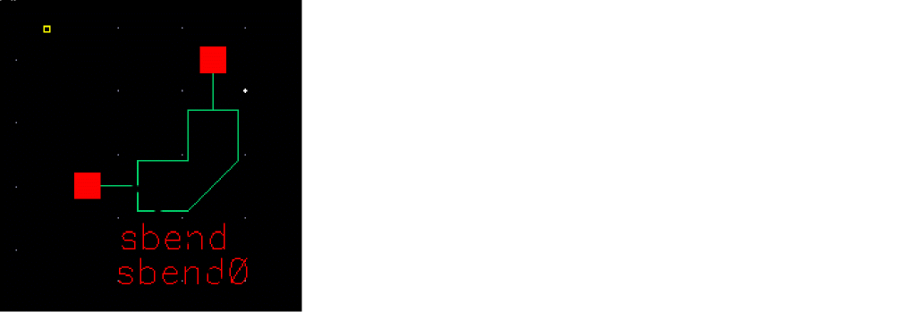
Microstrip bend with the specified angle and miter fraction
A bend instance must have exactly two transmission line instances connecting to its terminals, one transmission line per terminal. Both transmission lines should refer to the same stackup. It is an error to have instances of any other model connect to the terminals of a step.
The geometric and material information is obtained automatically from the transmission line instances.
The frequency-domain model is an empirically based model, which consists of a T-network of three impedances with two cascaded sections of transmission lines.
Command-line help
spectre -h bend
CDF Parameters
The miter fraction is defined as follows:
Draw a line from the inside vertex of the bend to the outside vertex of the unmitered bend. The miter fraction is the distance from the mitered edge at the intersection of the miter and the line to the outside vertex (labeled fraction below) divided by the total length of the line from vertex to vertex.

Range of Usage
The dielectric constant Er should satisfy the inequalities ![]() .
.
The ratio of the trace width W to the dielectric substrate thickness h should satisfy the inequality .![]()
The angle (in degrees) should satisfy the condition ![]() .
.
Example
mbend0 (net1 net2) bend angle=85 miterfraction=0.6
SYMBOL: MCORN
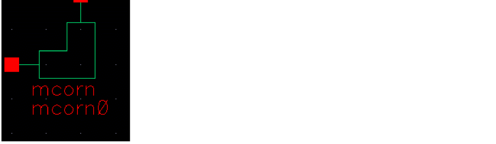
Microstrip unmitered 90 degree corner
A corner instance must have exactly two transmission line instances connecting to its terminals, one transmission line per terminal. Both transmission lines should refer to the same stackup. It is an error to have instances of any other model connect to the terminals of a step.
The geometric and material information is obtained automatically from the transmission line instances.
The frequency-domain model is an empirically based model which consists of a lumped equivalent circuit (T-network of two inductors and a shunt capacitor to ground). The equivalent circuit parameters are frequency-independent and are expressed as functions of trace width, dielectric height, and dielectric constant.
The expressions were developed by Kirschning, Jansen, and Koster and given in the following publication:
M. Kirschning, R. H. Jansen, and N. H. L. Koster. 'Measurement and Computer-Aided Modeling of Microstrip Discontinuities by an Improved Resonator Method', 1983 IEEE MTT-S International Microwave Symposium Digest, May 1983, pp. 495-497.
Command-line help
spectre -h corner
CDF Parameters
Range of Usage
The model, implemented as described in the reference given above, is valid for the ratio of the trace width W to the substrate thickness h within the range ![]() .
.
The dielectric constant Er should satisfy the inequality ![]() .
.
Example
mcorn0 (net1 net2) mcorn
SYMBOL: MCROS
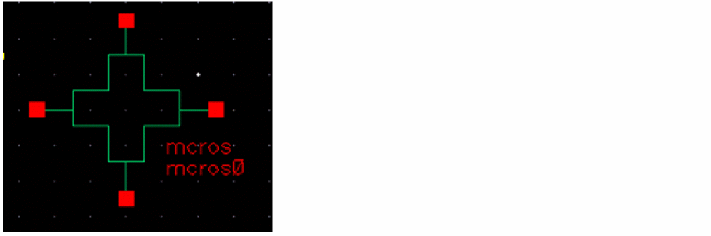
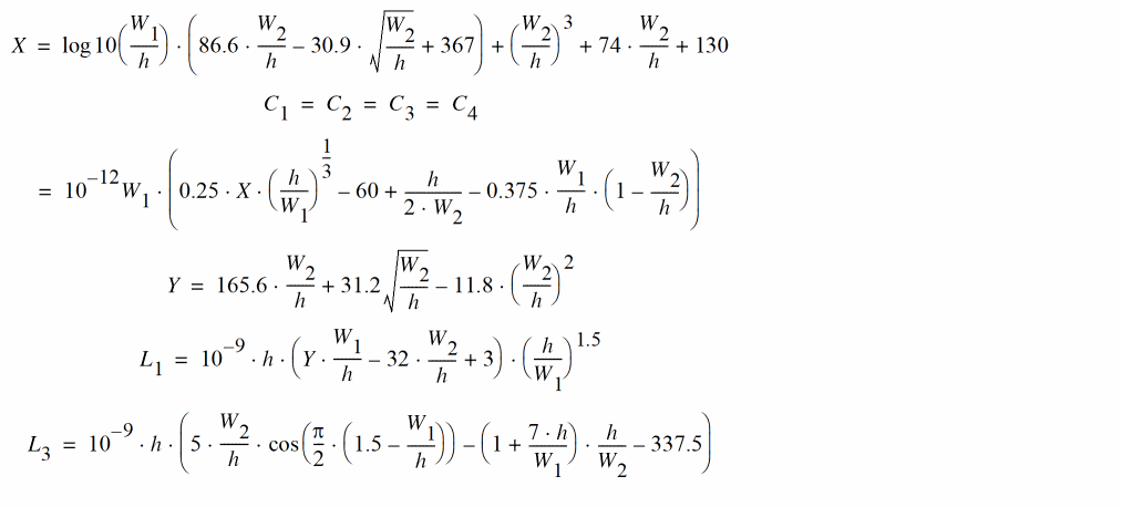
Microstrip cross
A cross instance must have exactly four transmission line instances connecting to its terminals, one transmission line per terminal. All four transmission lines should refer to the same stackup. It is an error to have instances of any other model connect to the terminals of a step.
The geometric and material information is obtained automatically from the transmission line instances.
The frequency-domain model is an empirically based model which consists of a lumped equivalent circuit (five inductors and four shunt capacitors to ground). The equivalent circuit parameters are frequency-independent and are expressed as functions of trace width, dielectric thickness, and dielectric constant.
A diagram of the physical cross and the equivalent circuit is shown below.

The model of a microstrip cross instance shows the equivalent circuit (right-hand side) and the layout with dimensions (left-hand side). The hatched area in the layout marks the area modeled by the equivalent circuit. As can be seen, the model requires the microstrip width of line 1 and 3, as well as the one of line 2 and 4 to be equal to each other. In addition, the permittivity of the substrate must be ![]() = 9.9 (Accommodation of different dielectric constants is shown later). The component values are calculated as follows:
= 9.9 (Accommodation of different dielectric constants is shown later). The component values are calculated as follows:
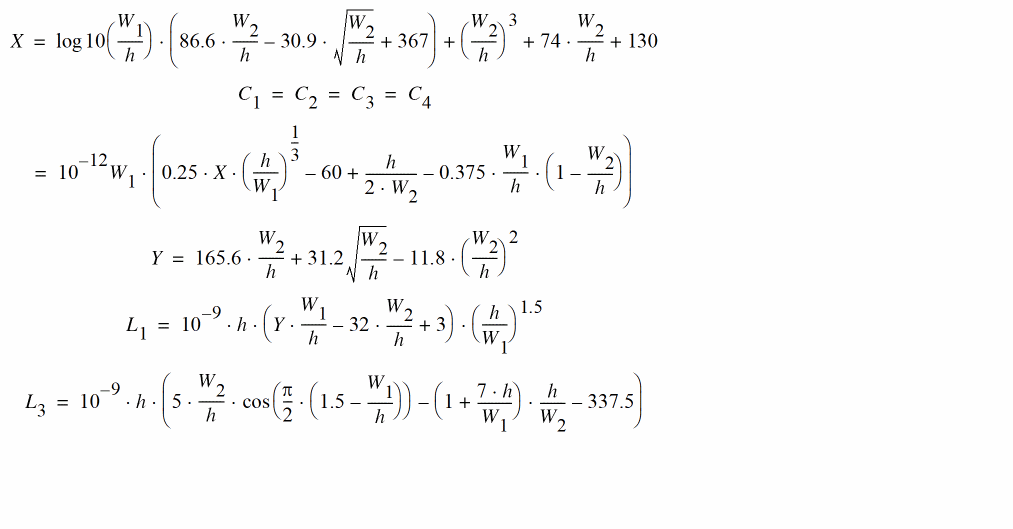
The equation of L2 is obtained from the one of L1 by exchanging the indices ( W1 and W2). Note that L3 is negative, so the model is unphysical without external microstrip lines. The above-mentioned equations are accurate to within 5% for ![]() and
and
![]() (value of C1 ... C4) or for
(value of C1 ... C4) or for ![]() (value of L1.... L3), respectively.
(value of L1.... L3), respectively.
Some improvements to this model include:
- Comparisons with real life show that the value of L3 is too large. Multiplying it by 0.8 leads to much better results.
-
The model can be expanded for substrates with
 by modifying the values of the capacitances, as follows:
where:
The equations of Z0 and are the ones from the microstrip lines.
The model assumes that there are only two distinct values of the trace width, w1Left=w1Right and w2Bottom=w2Top. Trace widths are defined as follows:
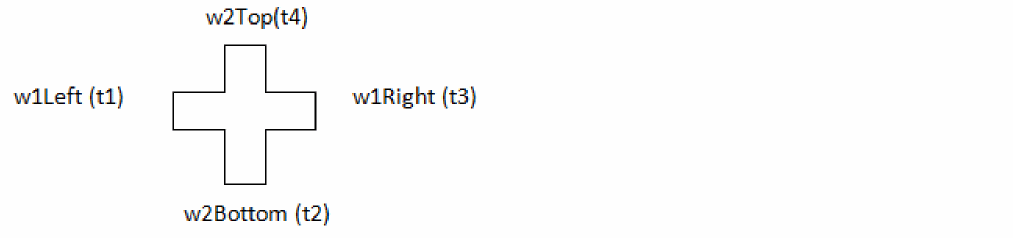
As an approximation, the geometric mean of the trace width,
W1=sqrt(w1Left * w1Right), W2=sqrt(w2Top * w2Bottom) is used if this condition is not satisfied.
Command-line help
spectre -h cross
CDF Parameters
Range of Usage
Denote the larger trace width as W1, and the smaller trace width as W2. The model has accuracy of approximately 5% if the following inequalities are satisfied:
Example
mcros0 (t1 t2 t3 t4) cross
SYMBOL: SCROS
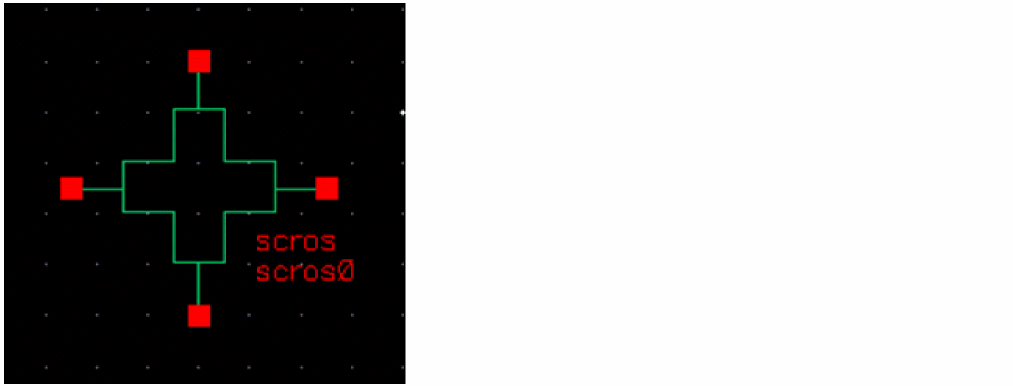
Stripline cross
A cross instance must have exactly four transmission line instances connecting to its terminals, one transmission line per terminal. All four transmission lines should refer to the same stackup. It is an error to have instances of any other model connect to the terminals of a step.
The geometric and material information is obtained automatically from the transmission line instances.
The frequency-domain model is an empirically based model which consists of a lumped equivalent circuit (five inductors and four shunt capacitors to ground). The equivalent circuit parameters are frequency-independent and are expressed as functions of trace width, dielectric thickness, and dielectric constant.
A diagram of the physical cross and the equivalent circuit is shown below.
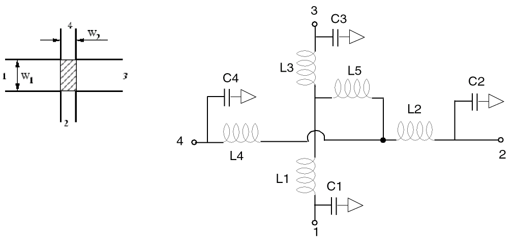
The model of a microstrip cross instance shows the equivalent circuit (right-hand side) and the layout with dimensions (left-hand side). The hatched area in the layout marks the area modeled by the equivalent circuit. As can be seen, the model requires the microstrip width of line 1 and 3, as well as the one of line 2 and 4 to be equal to each other. In addition, the permittivity of the substrate must be ![]() = 9.9. The component values are calculated as follows:
= 9.9. The component values are calculated as follows:
The equation of L2 is obtained from the one of L1 by exchanging the indices ( W1 and W2). Note that L3 is negative, so the model is unphysical without external microstrip lines. The above-mentioned equations are accurate to within 5% for ![]() and
and
![]() (value of C1 ... C4) or for
(value of C1 ... C4) or for ![]() (value of L1.... L3), respectively.
(value of L1.... L3), respectively.
Some improvements to this model include:
- Comparisons with real life show that the value of L3 is too large. Multiplying it by 0.8 leads to much better results.
-
The model can be expanded for substrates with
 by modifying the values of the capacitances, as follows:
where:
The equations of Z0 and are the ones from the microstrip lines.
The model assumes that there are only two distinct values of the trace width, w1Left=w1Right and w2Bottom=w2Top. Trace widths are defined as follows:
As an approximation, the geometric mean of the trace width,
W1=sqrt(w1Left * w1Right), W2=sqrt(w2Top * w2Bottom) is used if this condition is not satisfied.
Command-line help
spectre -h cross
CDF Parameters
Range of Usage
The simulation frequency f should satisfy the equation F[GHz] < Zo/B [mm], where Zo is the characteristic impedance, and B is the dielectric thickness (reference plane separation), in millimeters.
Example
scros0 (t1 t2 t3 t4) cross
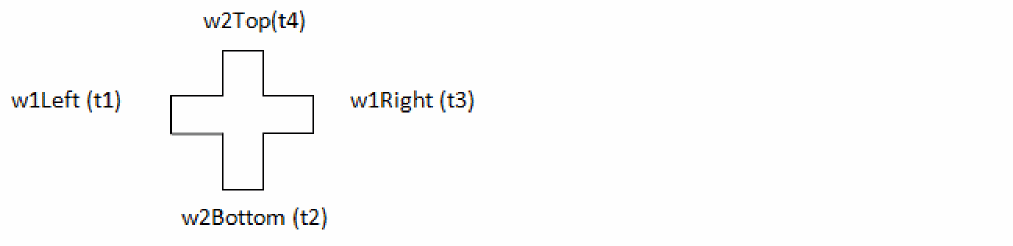
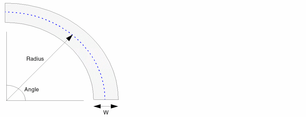
SYMBOL: MCURVE
Microstrip curve
A curve instance must have exactly two transmission line instances connecting to its terminals, one per terminal. Both transmission lines should refer to the same stackup. It is an error to have instances of any other models connect to the terminals of a curve.
The geometric and material information is obtained automatically from the transmission line instances.
The frequency-domain model is an empirically based model which consists of an equivalent transmission line.
The geometry of the mcurve model is defined in the figure below.

The default value of the radius parameter in this model is 0. This signals the model to set the radius r=2W, where W is the trace width.
Command-line help
spectre -h curve
CDF Parameters
Range of usage
The ratio of the trace width W to the substrate thickness h should satisfy the inequality
Due to the symmetry, the negative and positive values of Angle yield the same answer.
The radius r should be greater than W/2 (r=0 actually means to set r=2W and is also allowed).
Example
mcurve0 (net1 net2) curve
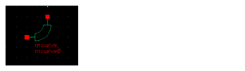
SYMBOL: SCURVE
Stripline curve
A curve instance must have exactly two transmission line instances connecting to its terminals, one per terminal. Both transmission lines should refer to the same stackup. It is an error to have instances of any other models connect to the terminals of a curve.
The geometric and material information is obtained automatically from the transmission line instances.
The frequency-domain model is an empirically based model which consists of an equivalent transmission line.
The geometry of the mcurve model is defined in the figure below.
The default value of the 'radius' parameter in this model is 0. This signals the model to set the radius r=2W, where W is the trace width.
Command-line help
spectre -h curve
CDF Parameters
Range of usage
The ratio of the trace width W to the substrate thickness h should satisfy the inequality
Due to the symmetry, the negative and positive values of Angle yield the same answer.
The radius r should be greater than W/2 (r=0 actually means to set r=2W and is also allowed).
Example
scurve0 (net1 net2) curve
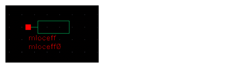
SYMBOL: MLOCEFF

Microstrip Open Circuit End Effect
The open end effect model mloceff accounts for the end effect of the microstrip transmission line (such as fringing capacitance). The typical usage involves connecting it to a microstrip transmission line. The mloceff model itself is not a transmission line model, and it has no length.
An mloceff instance must have exactly one transmission line instance connecting to its terminal. It is an error to have instances of any other models connect to the terminals of a curve.
The geometric and material information is obtained automatically from the transmission line instances.
The frequency-domain model is the transmission line length extension as described by Eqn. (4) in E. Hammerstad, "Computer-Aided Design of Microstrip Couplers with Accurate Discontinuity Models", IEEE MTT-S Symp. Dig., p. 54, 1981.
Command-line help
spectre -h loc
CDF Parameters
Range of usage
The model is sufficiently accurate (within 3%) for the ratio W/h <3, where W is the trace width, and h is the substrate thickness.
Example
mloceff0 (net1 net2) loc
SYMBOL: SLOCEFF
Stripline Open Circuit End Effect
The open end effect model mloceff accounts for the end effect of the microstrip transmission line (such as fringing capacitance). The typical usage involves connecting it to a microstrip transmission line. The mloceff model itself is not a transmission line model, and it has no length.
An mloceff instance must have exactly one transmission line instance connecting to its terminal. It is an error for instances of any other model to connect to the terminals of a curve.
The geometric and material information is obtained automatically from the transmission line instances.
The frequency-domain model is the transmission line length extension as described by Eqn. (6.2) in K. C. Gupta, R. Garg, R. Chadha, Computer-Aided Design of Microwave Circuits, Artech House, 1981, p. 187.
Command-line help
spectre -h loc
CDF Parameters
Range of usage
The ratio of trace with to the dielectric substrate thickness should not exceed 3.
Example
sloceff0 (net1 net2) loc
SYMBOL: CLIN
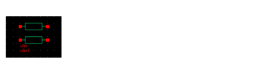
Lossless 2-Conductor Coupled Line
clin represents an ideal two-conductor coupled transmission line. clin is specified in terms of its even and odd-mode characteristic impedance, even and odd-mode electrical length, and the frequency at which the electrical lengths are specified.
Calculation procedure
Letting ![]() and
and ![]() represent the even and odd-mode electrical lengths in degrees, f represent the frequency at which the electrical lengths are measured, and letting the physical length of the line be 1m, the even and odd mode phase velocities
represent the even and odd-mode electrical lengths in degrees, f represent the frequency at which the electrical lengths are measured, and letting the physical length of the line be 1m, the even and odd mode phase velocities ve and vo are:

If the inductance and capacitance matrices of the line are expressed as:
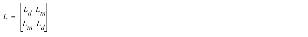
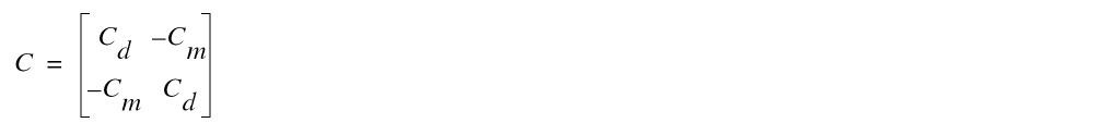
where Cm is positive, the matrix elements are given by:
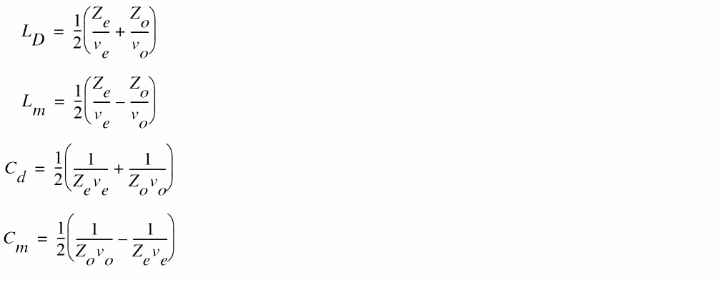
clin is netlisted as Spectre mtline with inductance and capacitance matrices, as specified in the above equations.
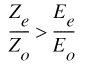
Parameter conditions
The clin parameters must satisfy the following conditions:
CDF Parameters
SYMBOL: TLINP
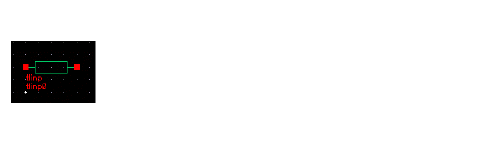
Single-conductor behavioral transmission line
tlinp represents a lossy single-conductor transmission line. The line is defined in terms of the following CDF parameters:
CDF Parameters
Notes
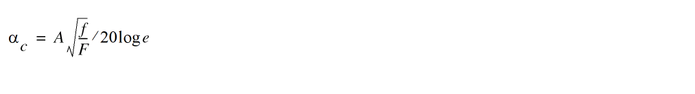
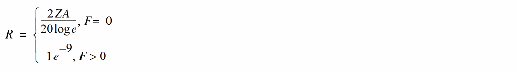
The characteristic impedance is specified at an infinite frequency (that is, ignoring loss).
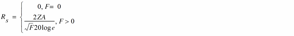
Attenuation in dB/m specifies the conductor loss factor. Considering F to be the reference frequency for attenuation, there are two modes of loss behavior with respect to frequency -constant and square-root dependent. In particular, when F=0,
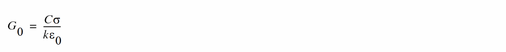
tlinp parameters are mapped to Spectre mtline parameters as follows:
tlinp1 (in out 0 0) mtline len=<Physical length> r=[(R)] l=[(L)] g=[(G0)] c=[(C)] rskin=[(Rs)] gdloss=[(Gd)]

-
 is the relative permeability
 - k is the specified effective dielectric constant
- c is the speed of light in vacuum
-
 is the specified dielectric conductivity in S
 -
 is the vacuum permittivity
 -
tandis the specified loss tangent - A is the specified conductor attenuation in dB/m
- F is the specified reference frequency
Parameter Conditions
The tlinp parameters must satisfy the following conditions:
Obsolete Components
The following are the obsolete elements contained in the RF transmission line library, rfTlineLib:
These components can be placed in a schematic to approximate the effect that the layout has on the operation of the circuit. When the schematic is netlisted, the tool generates an equivalent RLCG subcircuit for each rfTlineLib component and instantiates the new subcircuits in the design. This additional detail improves the accuracy of the simulation.
Placing the rfTlineLib components in the schematic requires you to provide information such as the widths and thicknesses of strips and the heights of substrates. The process of adding one of these components to the schematic opens a form where you provide the required information as CDF values.
Microstrip Components
A microstrip consists of a conducting strip that is separated from a ground plate by a substrate. The dielectric on the other side of the conducting strip is typically air.
microbend2
This is a microstrip chamfered right-angle bend.
|
Width of the microstrip, in meters. The width is the same on both sides of the bend and, in the symbol, is labeled as both |
The equivalent circuit is this.
microbend90
This is a microstrip right-angle bend.
|
Width of the microstrip, in meters. The width is the same on both sides of the bend and, in the symbol, is labeled as both |
The equivalent circuit is this.
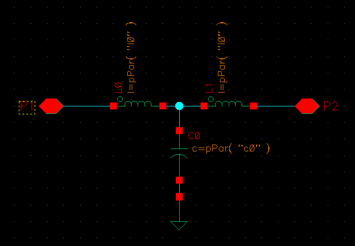
microopenend
This is a microstrip open end line.
|
Width of the microstrip, in meters. In the symbol, this is labeled |
|
|
Length of the microstrip, in meters. In the symbol, this is labeled |
|
The equivalent circuit is this.
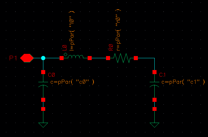
microstep
This component steps up or down the width of a microstrip.
|
Width of one side of the microstrip, in meters. In the symbol, this is labeled |
|
|
Width of the other side of the microstrip, in meters. In the symbol, this is labeled |
|
The equivalent circuit is this.
microstrip
|
Width of the microstrip, in meters. In the symbol, this is labeled |
|
|
Length of the microstrip, in meters. In the symbol, this is labeled |
|
The equivalent circuit is this.
Stripline Components
A stripline consists of a conducting strip that is sandwiched between two ground planes but separated from each of them by a substrate layer.
stripbend90
This is a stripline right-angle bend.
|
Width of the stripline, in meters. The width is the same on both sides of the bend and, in the symbol, is labeled as both |
|
The equivalent circuit is this.
stripline
|
Width of the stripline, in meters. In the symbol, this is labeled |
|
|
Length of the stripline, in meters. In the symbol, this is labeled |
|
The equivalent circuit is this.
Return to top