2
Getting Started with SPD
This section covers the following topics:
- Generating a Symbolic Placement
- SPD Editing Window
- Highlighting and Selecting Data
- Understanding the Symbolic Design
- Saving an SPD Design
- Exiting the SPD Editing Window
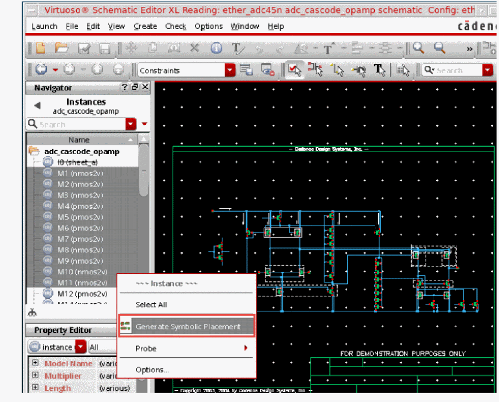
Generating a Symbolic Placement
You can open a design in SPD directly from Schematics XL or from Layout XL:
Generating a Symbolic Placement from Schematics XL
Generating a Symbolic Placement from Layout XL
- Select instances of PMOS and NMOS devices in Layout XL for which you want to generate the symbolic design.
-
Click the Generate Symbolic Placement icon on the toolbar. In case, this icon is not available on the toolbar, right-click in the toolbar area, and then select the Symbolic Placement of Devices menu option.
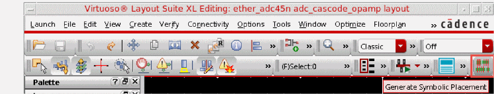
-
The SPD Editing window opens displaying the symbolic design of selected devices.
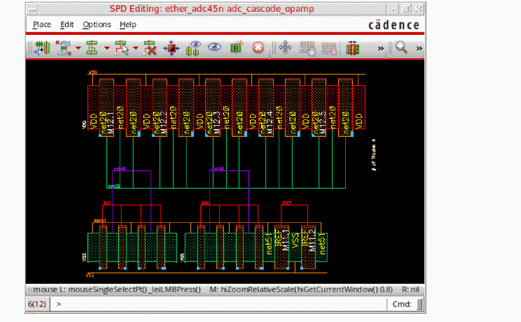
SPD Editing Window
The SPD Editing window comprises a menu bar, toolbars that let you use various SPD commands at a single-click and a canvas, in which you can display and manipulate your symbolic design graphically.
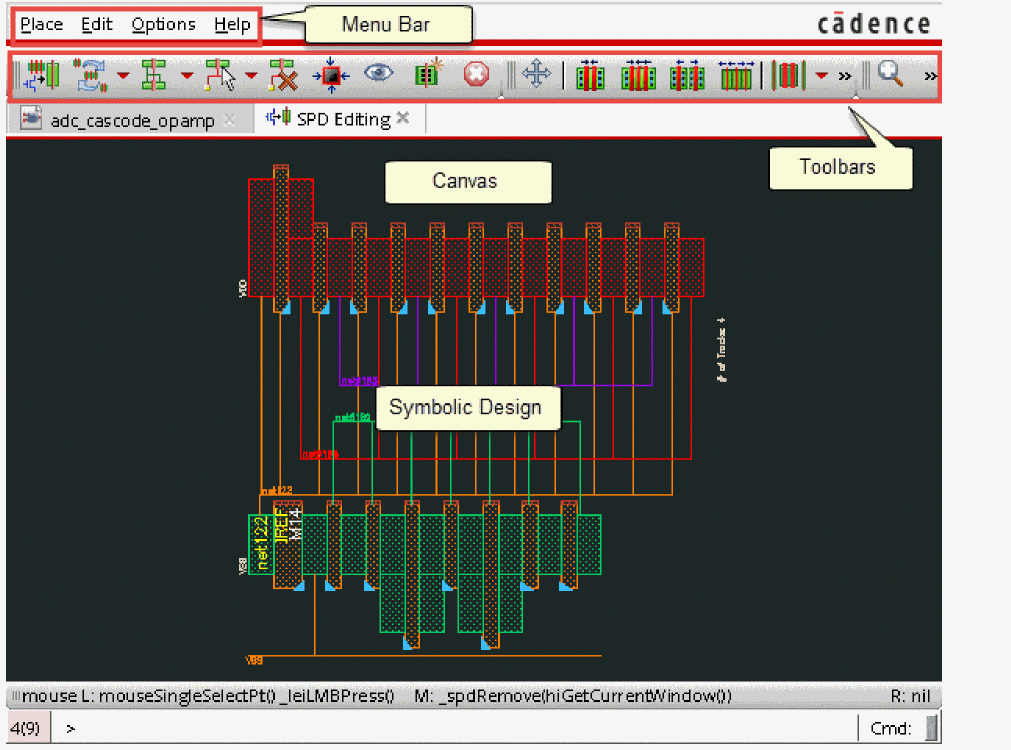
Menus
There are four menus in the SPD window. Place, Edit, and Options menus comprise various commands to enable you to perform various edit and placement tasks. The Help menu lets you access the help documentation.
Toolbars
SPD toolbars lets you access the main SPD commands directly without opening any menus. As with all toolbars, you can use the handle on the left hand side of the toolbar to reposition it anywhere within the layout window.
The Place Toolbar
The Place toolbar provides access to the following Place menu commands:
|
Add new devices to the SPD design from the source schematic. See Appending Components from the Schematic for more information. |
||
|
Discard any placement changes made to the symbolic design and revert to placement set in the SPD Options form. See Resetting Placement for more information. |
||
|
Control how flight lines are displayed in the SPD canvas. See Displaying Flight Lines for more information. |
||
|
Select nets in the symbolic design to highlight the corresponding element in the schematic window. See Probing Selected Nets for more information. |
||
|
Clear all probes highlighted in the SPD canvas. See Probing Selected Nets for more information. |
||
|
Remove empty spaces from the design. See Packing the Design for more information. |
||
|
Toggle the free bucket size mode. See Displaying Free Bucket Size of Devices for more information. |
||
|
Preview the physical layout of the symbolic design. See Previewing the Design for more information. |
||
|
Generate the final layout and place it in the Layout XL canvas. See Generating the Layout for more information. |
||
|
See Exiting the SPD Editing Window for more information. |
The Edit Toolbar
The Edit toolbar provides access to the following Edit menu commands:
|
Move symbolic devices from one location to another in the canvas. See Moving Symbolic Devices for more information. |
||
|
Reorder trunks before generating the layout. See Reordering Trunks for more information. |
||
|
Reset the modified trunk order. See Resetting Trunk Order for more information. |
||
|
Abut selected devices or device chains. See Abutting Devices for more information. |
||
|
Abut all devices in the canvas. See Abutting All Devices for more information. |
||
|
Unabut selected devices or device chains. See Unabutting Devices for more information. |
||
|
Unabut all abutted devices in the canvas. See Unabut All Devices for more information. |
||
|
Add dummy devices to the design. See Adding Dummy Devices for more information. |
||
|
Add the newly added dummy devices to schematic. See Backannotating Symbolic Devices for more information. |
||
|
See Undoing and Redoing Commands for more information. |
||
|
Reinstate a change that you canceled with Undo. See Undoing and Redoing Commands for more information. |
||
|
Flip selected device or device chains horizontally. See Flipping Symbolic Devices for more information. |
||
|
Flip selected device or device chains vertically. See Flipping Symbolic Devices for more information. |
||
|
Permutes the devices without changing the orientation. See Permuting Symbolic Devices for more information. |
||
|
Swap the positions of symbolic instances. See Swapping Symbolic Devices for more information. |
||
|
Divides symbolic instances into two or more layout instances such that their terminals are connected in parallel to the same nets. See Folding Symbolic Devices for more information. |
||
|
Place each finger of a symbolic finger device as a separate device. See Splitting Fingered Devices for more information. |
||
|
See Removing Symbolic Devices for more information. |
||
|
See Aligning Symbolic Devices for more information. |
||
|
See Unaligning Devices for more information. |
||
|
Identify misalignments in the symbolic design. See Checking Device Alignment for more information. |
||
|
See Generating Chained Devices for more information. |
||
|
See Stacking a Device for more information. |
||
|
See Unstacking a Stacked Device for more information. |
||
|
See Editing a Stacked Device for more information. |
Other Toolbar Commands
|
Magnifies the image in the cellview window by a factor of 1.25. You can also scroll up the mouse scroll wheel to zoom in. |
||
|
Reduces the image in the cellview window by a factor of 20.8. You can also scroll down the mouse scroll wheel to zoom out. |
||
|
Redraws the window so that all objects in the cellview appear in the window. This saves time after you zoom or pan and want to see the entire cellview again |
||
|
Check the differences between the source and SPD layout, or update existing objects in the SPD window. See Checking Source or Updating Layout for more information. |
Canvas
The canvas is always visible in the SPD editing window. It shows the symbolic design of the abstract devices arranged in rows. You can perform various device editing and placement tasks, such as abutting, folding, and stacking devices from here.
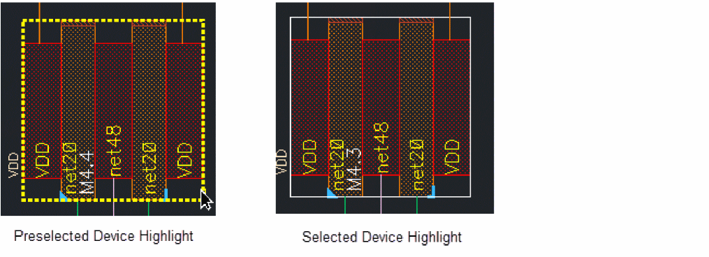
Highlighting and Selecting Data
Highlighting and selection of devices in SPD is the same as in Layout XL. Preselected devices are highlighted with dashed yellow line and selected devices are highlighted with white line.
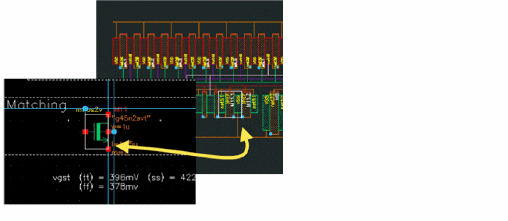
When you select a device in SPD, its corresponding device is automatically selected in the schematic:
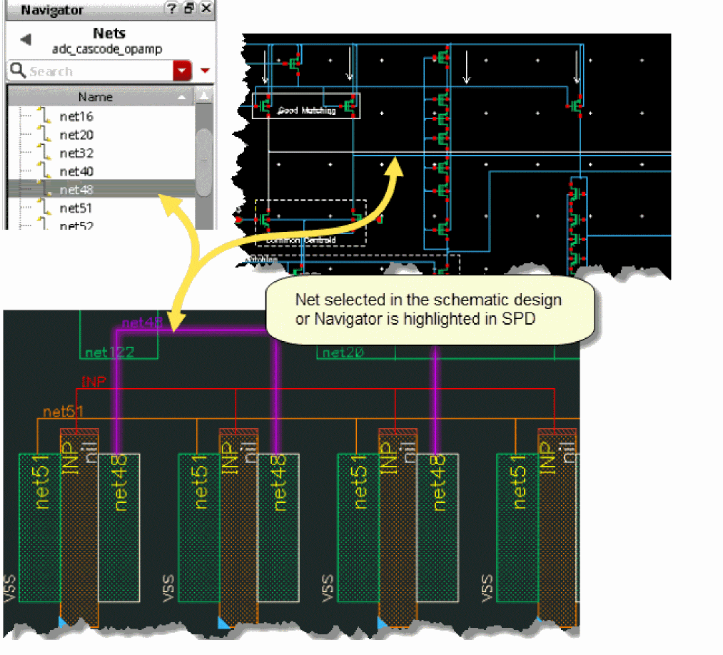
When you select a net in the schematic design or Navigator, its corresponding net is automatically highlighted in the SPD Editor window:
Understanding the Symbolic Design
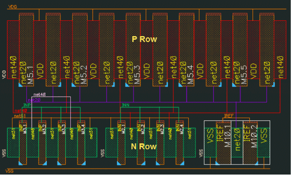
The row-based, symbolic layout generated in SPD shows only the required information and does not show all the layers.
Row-based Placement
By default, when you generate the symbolic layout, devices are arranged in an NP row pattern. The top row (P row) of the design, represented in red, contains the PMOS devices and the bottom row (N row), represented in green, contains the NMOS devices.
Support for Multiple Rows
SPD enables you to add more number of rows and move devices to these rows based on your requirement. Some of the multi-row patterns supported by SPD include: NP, PN, NPPN, PNNP, NPNP, PNPN, NNPP, PPNN, NNNP, PNNN, NPPP, PPPN, NNNN, and PPPP. SPD can group instances with same bulk nets at the same row or at a near location during initializing SPD in the multiple row flow.
Device Representation
When a symbolic layout is generated from a schematic, all information that is not needed is hidden. What you see in the design are symbols that comprise the drain, source, and gate of each P-type or N-type transistor.
In the figure below, the drain of the symbolic device is displayed on the right side, the source on the left and the gate is located in between. Each component is labeled with the name of the net to which it is connected. The gate also shows name of the instance and you can choose to display the size of the device, which is not displayed by default.
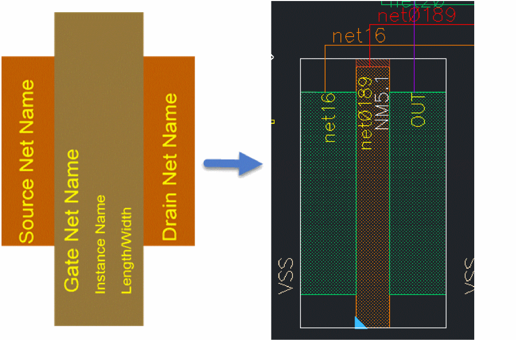
In the above image, you can see that the name of the instance is NM5.1, which is connected between net16 and OUT.
Devices of Different Sizes
Instead of displaying the exact sizes of each abstract device, SPD shows their relative sizes by automatically categorizing the device sizes into small, medium, and large sizes based on their widths. Each category can include devices of different sizes as you can see in the screenshot below.
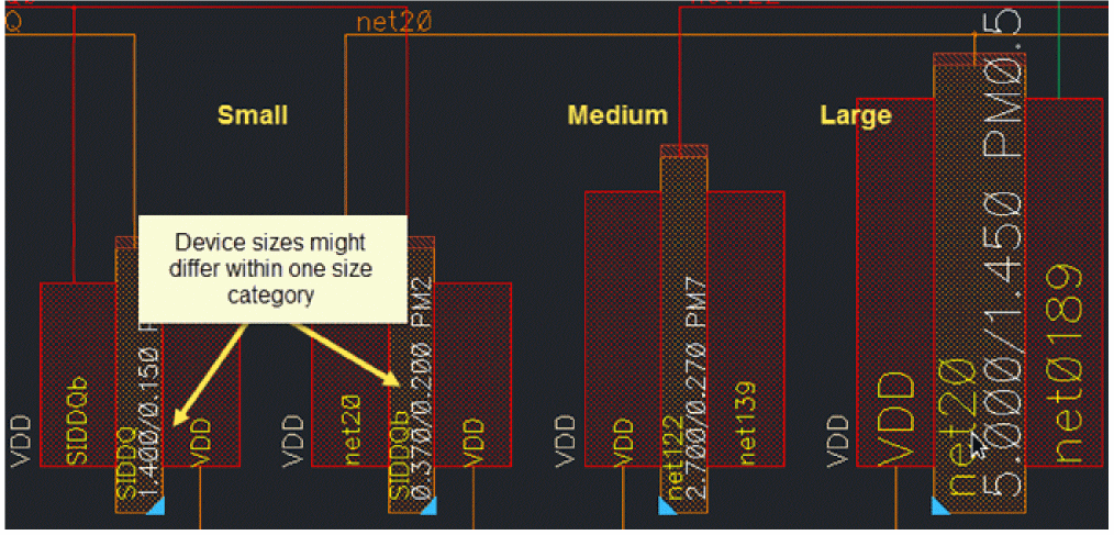
There are three ways in which you can find out the real size of the devices:
- View the size label for each device. These labels are not displayed by default. You can enable them from the Display Options pane.
- View the actual size in the schematic. When you select a device in the SPD window, the device is cross-selected in the schematic window is automatically selected, making it simpler to view its actual size.
-
Enable the Free Bucket Size option to display the symbolic device in proportion to its real size. When you use this option, the design can approximately look like the actual layout. See Displaying Free Bucket Size of Devices for more information.
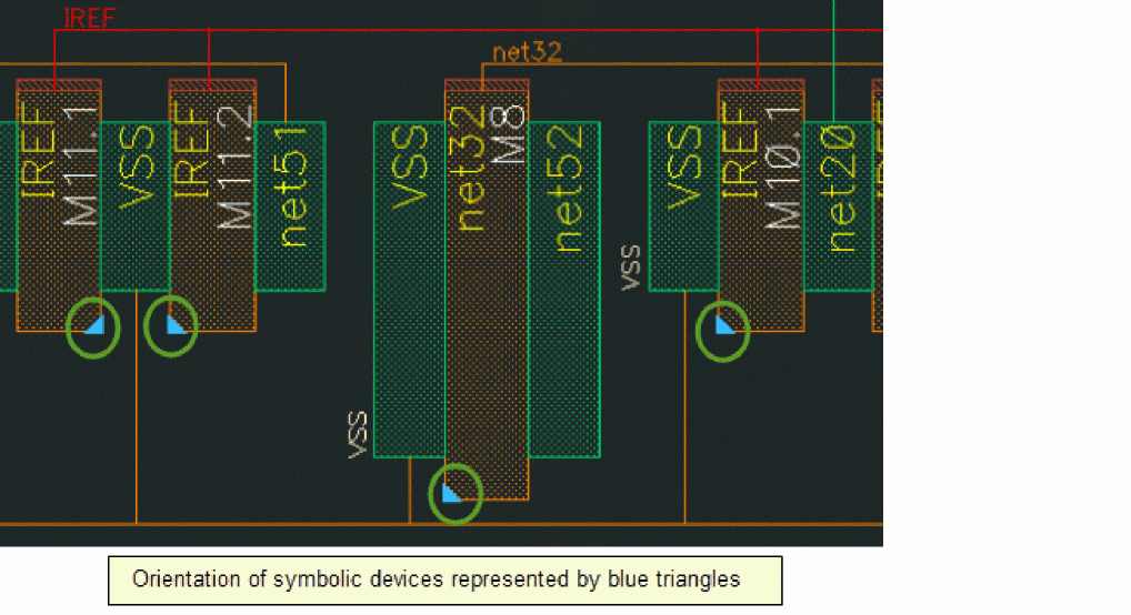
Device Orientation
Orientation of a symbolic device is indicated using a blue triangle. The size of these triangles is the same regardless of device sizes. The orientation of the symbolic device in the figure below is R0.
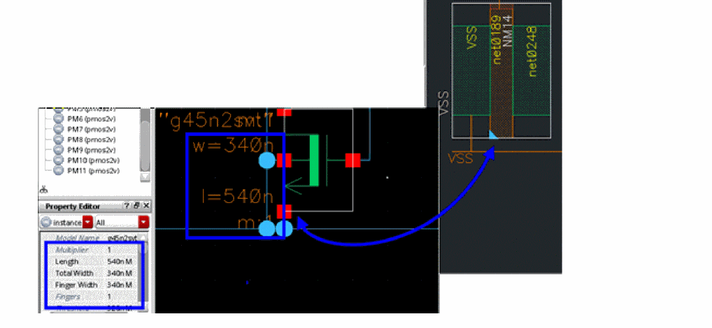
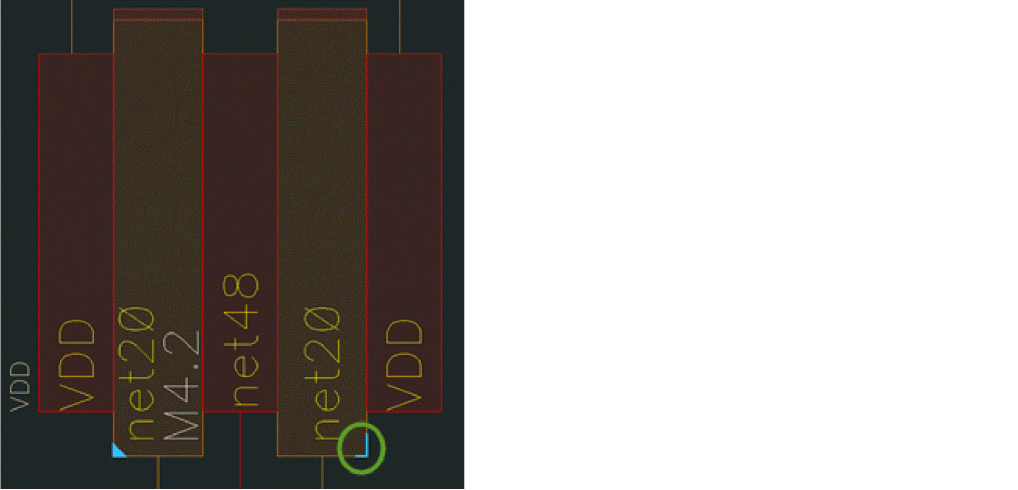
Device Fingers
An instance that contains several fingers is identified by a blue L-shape. The first finger of the device is marked with a blue triangle and the last finger is identified by a blue L-shape. In the image below, you can see an instance with two fingers.
Displaying Flight Lines
The symbolic design displays flight lines in the channel area between the P and N rows. These flight lines are not real physical design objects and therefore they cannot be selected or modified. They depict logical connections between the drain, gate, and source pins of the devices.
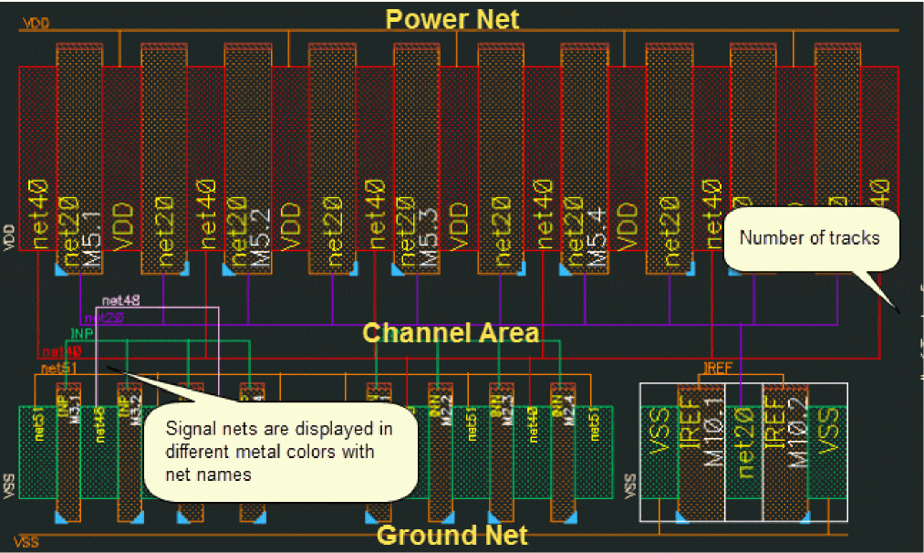
- Power and ground nets are displayed by default in the design, in a single color.
- The number of tracks appears at the right of the channel area. The height of the channel area is also symbolic and remains fixed even if the number of tracks changes when the design is edited.
- Signal nets are displayed in the appropriate metal layer color in the channel area along with their net names.
Abutment
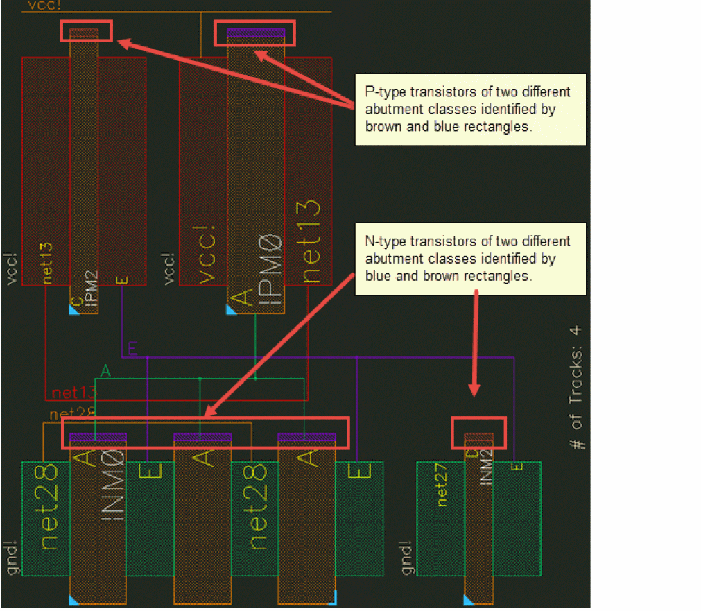
Abutment Class of Devices
Symbolic devices of different masters or different abutment classes are identified by small rectangles drawn in different colors at the top of the gate. Instances of different abutment classes cannot be abutted.
In the image below, P-type transistors and N-type transistors of two different abutment classes, are identified by brown and blue rectangles.
For more information on abutment class, refer
User Defined Abutments
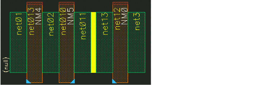
You can define PDK-specific abutments that is different from the regular oxide diffusion (OD) abutment, for example the dummy poly abutment. A user-defined abutment is identified by a rectangle between the source and drain of two abutted instances. The color of the rectangle indicates the type of user defined abutments. Different colors denote different types of user-defined abutments.
In the image below, you can see a yellow rectangle between instance NM5 and NM0, which denotes that NM5 abuts NM0 by a user-defined abutment. While NM4 and NM5 is the regular oxide diffusion abutment.
For more information, see Abutting and Unabutting Symbolic Devices.
Stacked Devices
SPD can stack multiple instances together. To indicate the bottom instance of a set of stacked devices, the gate of the bottom instance is drawn in dark blue and the names of stacked instances are shown on the gate.
In the image below, you can see instance PM4 is stacked by PM2 and PM1.
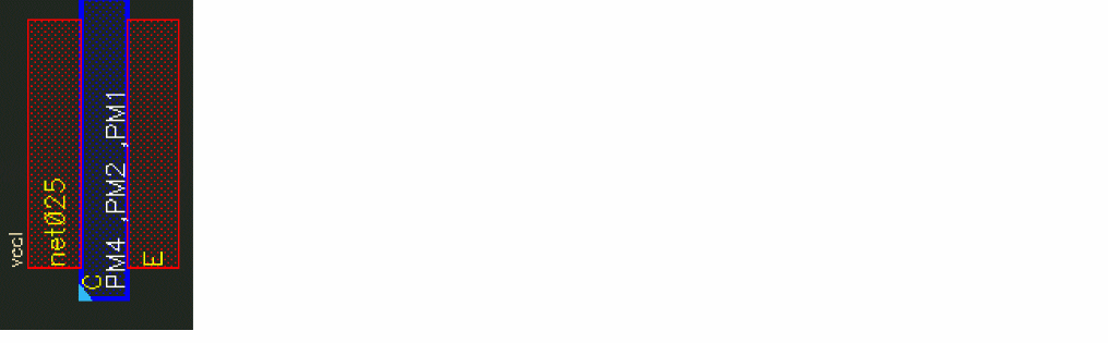
For more information, see Stacking Symbolic Devices.
Saving an SPD Design
-
Choose Place – Save [
F2].
The Save SPD Design form is displayed.
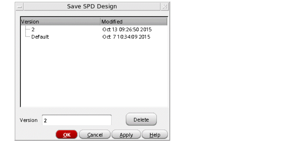
- Specify the version number for the design. You can also select an existing version number from the Version list in the form.
- Click OK.
Design with the specified version number is saved.
If there are several designs listed in the Save SPD Design form, you can perform the following tasks to sort the designs:
- Click the header of the Version column to sort designs by the version number.
- Click the header of the Modified column to sort the designs by the modification time.
Click any of the header columns two times to change the sorting direction.
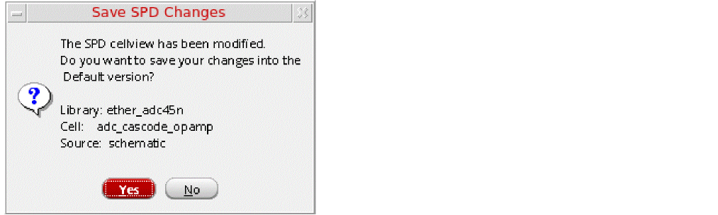
The following dialog box will be displayed if you try to exit SPD without saving the design.
If you save a design when the Options – SPD – Placement – Auto pack in X direction check box is not selected, then any extra spacing in the design is also saved. This spacing is restored when you load the design for further editing.
Exiting the SPD Editing Window
Choose Place – Exit [Ctrl+w] or click the Exit button on the SPD toolbar to close the SPD Editing window.
Return to top