A
Symbolic Placement of Devices Forms
This section lists the Virtuoso® Symbolic Placement of Devices (SPD) forms.
- Abut
- Align
- Append Selected from Source
- Check or Update
- Dummy Options
- Edit Stack
- Flip Horizontal
- Generate Chained Devices
- Generate Folded Devices
- Generate Layout
- Load SPD Design
- Move
- Probe & Align
- Save SPD Design
- SPD Options
Abut
Use the Abut form to set the preferred direction for abutment when one chain is inserted into another chain.
Preferred direction lets you choose to abut the left or right half of the target chain by selecting the appropriate radio button.
Related Topics
Abutting and Unabutting Symbolic Devices
Align
Use the Align form to control the alignment of gates between two rows.
Show flight lines of gates specifies whether to display flight lines during alignment. This check box is selected by default.
Related Topics
Append Selected from Source
Use the Append Selected from Source form to specify placement mode for the new devices being added to the SPD design from the source schematic.
Placement Mode specifies the mode for adding the devices.
Auto places the devices based on the current row pattern. This row pattern follows the pattern in layout and is detected when SPD is launched. You can change this pattern through SPD Options form.
Sort by Schematic X detects row pattern from schematic, and then sorts and places the devices from left to right.
Sort by Schematic Y detects row pattern from schematic, and then sorts and places the devices from bottom to top.
Related Topics
Appending Components from the Schematic
Check or Update
Use the Check or Update form to check the differences between the source and the SPD layout, or update existing objects in the SPD window.
|
checks the differences between the schematic and layout using the options available in the Check section. Use these options to choose what types of differences you want to see in the report and what format the report should take. |
|
|
automatically updates the SPD layout to take account of instances, pins, and connectivity you have changed in the schematic using the options available in the Update section. |
|
|
reports SPD instances that are not bound to schematic instances. |
|
|
reports connectivity issues on top level pins and global nets; mismatched or missing terminals and instance terminals; and unbound nets in SPD. |
|
|
reports issues with CDF parameters. You can specify how the parameters are compared on the |
|
prints the report in a separate Info window, otherwise the report is printed in the CIW.
Update
Selected layout components only updates only the instances and pins currently selected in the layout window.
Layout parameters automatically updates the parameters and parameter values on SPD instances to match those on their schematic counterparts. Parameters that are set in SPD instances but are not present on their schematic counterparts are not removed.
Related Topics
Checking Source or Updating Layout
Dummy Options
Use the Dummy Options form to configure how dummy instances are added to the symbolic design.
Net specifies the net name to which you want the dummy device to be tied. All terminals of a dummy instance, except its bulk terminal, are connected to the tie net.
Environment variable:
Dummy Parameters specifies the number of fingers and length and width of the dummy.
Number of Fingers sets the number of fingers for the dummy.
Environment variable: spdDummyNumFingersOptions
CDF Default sets the number of fingers to be the same as the default CDF parameter values. This is the default setting.
Same as Neighbor sets number of fingers to be the same as the neighboring instances.
Specify lets you specify the number of fingers manually in the text field that is displayed when you select this option.
Environment variable: spdDummyNumFingersValue
Length specifies the length for the dummy.
Environment variable: spdDummyLengthOptions
CDF Default sets the length to be the same as the default CDF parameter values. This is the default setting.
Same as Neighbor sets the length to be the same as the neighboring instance.
Specify lets you specify the length manually in the text field that is displayed when you select this option.
Environment variable: spdDummyLengthValue
Width specifies the width for the dummy.
Environment variable: spdDummyWidthOptions
CDF Default sets the width to be the same as the default CDF parameter values.
Same as Neighbor sets the width to be the same as the neighboring instance. This is the default setting.
Specify lets you specify the width manually in the text field that is displayed when you select this option.
Environment variable: spdDummyWidthValue
Remember Values specifies that the values set on the Dummy Options form are saved and remembered the next time the form is opened. This option is not selected by default.
Environment variable:
Related Topics
Edit Stack
Changes the placement of stacked instances.
Related Topics
Flip Horizontal
Use the Flip Horizontal form to specify whether to use pin permutation when flipping devices.
Permute lets you flip instances by pin permutation. By default, this check box is not selected.
For more information on how pin permutation works, see
Related Topics
Generate Chained Devices
Use the Generate Chained Devices form to generate a device chain when more than one
I/O pin-connected PMOS or NMOS devices are selected.
Select one of the devices in each list to specify the locations at which the respective device chains are to be placed.
Related Topics
Generate Folded Devices
Use the Generate Folded Devices form to control interactive folding, which lets you divide an individual transistor or a chain of transistors into two or more folds. Folding lets you change the aspect ratios of the devices in your design while retaining the original orientation. The devices to be folded need not be bound to a schematic instance.
Transistor Name shows the name of the transistor to be folded. If you have selected more than one transistor, use the Next and Previous buttons to move through the selected set.
Transistor Width shows the value of the width property of the selected device, indicating also whether the value is taken from the schematic or layout view. This option is available when the selected devices for folding are MOS transistors that have the Width parameter set.
Transistor Fins shows the value of the Number of fins parameter of the selected FinFET device, also indicating whether the value is taken from the schematic or the layout view.
Number of Folds lets you type in the number of folds for the selected device. Enter a value greater than one in this field and then click the Show Folds button, which evenly distributes the transistor width across the available folds.
Fold Threshold specifies the maximum size of a folded transistor. Enter a value and then , click Show Folds to spli t the transistor width into folds according to the specified threshold.
Chain Folds tells SPD to chain the resultant folds together where possible.
Hide Folds and Show Folds buttons let you hide or display the section that shows how the width or fins have been split across all folds.
Total Width shows the total value of all the fold widths displayed in the Width fields at the bottom of the form.
Add Fold adds an additional fold to the device and provides a field where you can specify the Width for the new fold.
Distribute evenly divides the total width of the transistor by the number of folds and sets the resultant Width as the value for each fold.
Delete removes the corresponding fold from the device.
The system automatically adds the Transistor Width unit identifier to any width value with no unit. If the Transistor Width has no unit identifier, no identifier is added to the Width fields. See
Related Topics
Generate Layout
Use the Generate Layout form to generate a physical layout of the symbolic design to a target Layout XL window.
Mode specifies the method used to generate the layout.
Coordinates places the origin of the layout in the SPD Preview window at the absolute coordinates of the target layout. You specify the absolute coordinates in the X and Y fields.
Delta to lower-left origin places the origin of the lower-left instance of the generated layout to the target Layout XL window at the origin where it was placed before it was updated in SPD. The origin is offset by values specified in the X and Y fields.
Delta to mouse lets you specify the origin of the lower-left instance of the generated layout by clicking in the canvas. The origin is offset by values specified in the X and Y fields.
Load SPD Design
Use the Load SPD Design form to load a previously saved SPD design. The selection box at the top of the form lets you select the version of the saved design you want to open. A preview of the selected design is shown in the bottom section.
Related Topics
Move
Use the Move form to control how the move operation is performed, including the angles at which you can move the object, the presence of draglines on the object as you move it, and the orientation of the object you select.
For information about the Move options, see the
Related Topics
Probe & Align
Use the Probe & Align form to find and highlight logical connectivity between selected nets.
The Show dropdown list lets you list All Nets or Pin Nets in the list box given below. You can choose one or more nets to highlight their logical connectivity in the design.
Sort specifies whether nets are listed in Ascending or Descending order in the list box.
|
Aligns the gates of the left most instances of the selected net in each row. |
|
Related Topics
Save SPD Design
Use the Save SPD Design form to save different versions of your SPD design.
Version specifies the version number for the saved design. This version and the date on which it was modified is displayed in the information box located in the upper part of the form.
Delete removes the version specified in the Version field.
Related Topics
SPD Options
The SPD Options form comprises a tree that lets you access the following option panes to further customize the symbolic layout of devices:
Placement Options
Use the Placement pane to configure chaining and folding options for the selected instances, and to specify row patterns and alignment for these instances.
The Chaining/Folding section lets you optimize the layout by abutting selected MOS transistors into chains, folded devices, or folded chained devices.
Chain automatically abuts the selected set of MOS transistors to form a chain. The transistors to be abutted must be set up for abutment first. For more information, see Setting Up Pcells for Abutment in Virtuoso Layout Suite XL User Guide.
Environment variable: initDoChaining
Fold automatically divides MOS transistors into folds to optimize utilization.
Environment variable: initDoFolding
Chain Folds automatically chains the individual folds of a transistor.
Interdigitate Chains automatically identifies nodes that qualify as pseudoparallel connections and defines them accordingly during chaining and abutment. A pseudoparallel net connects nodes that are always the same voltage, so current does not pass through the net.
NMOS Fold Threshold is the maximum size of the folded NMOS transistor.
Environment variable: foldingThresholdNType
PMOS Fold Threshold is the maximum size of the folded PMOS transistor.
Environment variable: foldingThresholdPType
Placement section lets you specify how PMOS and NMOS devices are placed in the design.
Row Pattern sets the row order for placement of devices. SPD supports the following two-row and multiple row device placement patterns: NP, PN, NPPN, PNNP, NPNP, PNPN, NNPP, PPNN, NNNP, PNNN, NPPP, PPPN, NNNN, PPPP, and (Arbitrary). The default is NP.
Row Number lets you specify the number of rows in the text field. This option is available when Row Pattern is set to (Arbitrary). The default is 10.
When this setting is used, PMOS devices are treated as NMOS devices and are represented with a white cap at the top.
Mix P//N in one row specifies whether both P and N type devices can be specified in a single row.
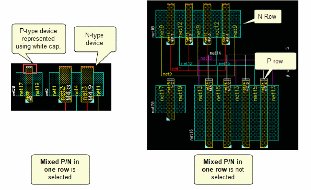
Environment variable: PNmixedRow
When you specify the row pattern as (Arbitrary) and specify four or more rows, the specified number of rows is used for the selected instances. However, if you have mixed P-type and N-type devices in a row and the Mix P/N in one row option is not selected then a dialog box is displayed that lets you either enable the Mix P/N in one row option or reset the placement.
Chain Alignment specifies how the instances in the chain are aligned. Choose one of the following:
Inside aligns instances to that side of a P or N row that is close to the channel area.
Outside aligns instances to that side of a P or N row that is far from the channel area.
Center aligns instances to the center of a P or N row.
Align to Gates sets the side of the gate to which the selected instance are aligned. You choose between Left, Center, and Right. The default is Center.
Auto gate alignment specifies whether to try to align the first gate of a chain with another gate even if no alignment has been specified in the symbolic design. This check box is selected by default.
Environment variable: autoAlignGates
For more information, see Aligning Symbolic Devices.
Priority specifies the placement for the priority devices in the chain.
Environment variable: placementPriority
Maximize OD Sharing optimizes the generated chains by maximizing oxide diffusion sharing.
Minimize number of tracks optimizes the generated chains by minimizing the number of tracks in the chained devices.
Auto automatically sets the placement priority. This is the default.
Pin Driven enables pin driven placement and optimizes the device placement according to the pin order you specified. By default, this check box is not selected. Pin driven placement can be used only for NP and PN row patterns. The option is disabled when you choose any other row pattern.
Environment variable: pinDriven
Order lets you manually specify the pin order from left to right for the pin driven placement. The figure below shows different ways in which pin order can be specified.
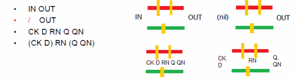
- Specify pin order from left to right.
- Separate pin names by spaces.
- The two ends of the pin order are assumed to be two edges of the placement. Therefore, the left most pin is assumed to be on the left edge of the placement and the right most pin is assumed to be on the right edge of the placement. In the above example:
-
/denotes an unspecified pin for one of the two ends. This works when there are only two pins in the pin order. -
()groups multiple pins. Pins in the same group are at the same position. In the example(CK D) RN (Q QN), PinsCKandDand pinsQandQNare at the same position.Although it is not mandatory to perform pin driven placement with an empty pin order list, it is recommended that you always specify pin order when you enable pin driven placement to have a meaningful result. Environment variable: pdPins
- Abut same width only abuts devices of same width. When this option is set all commands that perform automatic abutment, such as Reset Placement, Abut, Abut All, and Move, will abut only those devices that have same width.
Auto flip chain in 'Abut All' command automatically flips the chain when you select the Abut All command. Environment variable: abutAllAutoFlipChain
Move to insert in one location moves selected instances to the specified location in the design. By default, this check box is selected. Environment variable: smartMoveInsertOnePos
Auto pack in X direction automatically packs devices in horizontal direction when commands Move, Undo, Redo, Align, Save, and Load are used to change the position of devices. When this option is deselected, automatic packing does not take place. Environment variable: autoPackInX
Related Topics
Display Options
Use the Display options pane to specify how labels and flight lines are displayed in the design. You can also specify the dimensions considered to be medium-sized devices. The sizes for small and large devices are also derived from these values.
Label Display specifies what information is included in the labels for abstract devices. You can choose from:
The default value is All except Device Size.
Environment variable:
Show flight lines specifies that flight lines are displayed in the design. By default, this check box is selected.
Connect to sets the connectivity mode of flight lines. This option is available only when the Show flight lines option is selected.
Environment variable:
Gate displays flight lines for connections to gates.
Active displays flight lines for connections to the active region.
Both displays flight lines for connections to both gates and the active region. This is the default.
Connect between specifies the type of flight lines to display in the symbolic design. This option is available only when the Show flight lines option is selected and a multiple-row pattern, such as NPPN or PNNP is set for the Row Pattern option in the Placement options pane.
Environment variable:
1 row displays flight lines for connections within 1PN rows.
2 rows displays flight lines for connections between 2PN rows.
Both displays flight lines of both types. This is the default.
Show P/G Nets specifies how to display power and ground nets in the design.
None disables the display of power and ground flight lines.
Environment variable: showPGFlightLines
Separate displays power and ground (P/G) nets separate from signal nets at the bottom and the top of a PN row. When this option is selected, SPD still creates the P/G nets in channel. You need to specify the names of these nets in the Connectivity form or through Layout XL environment variables lxGroundNetNames and lxSupplyNetNames.
Mixed with signals mixes power and ground nets with signal nets in the channel area.
Environment variable: mixPGFlightLinesSignals
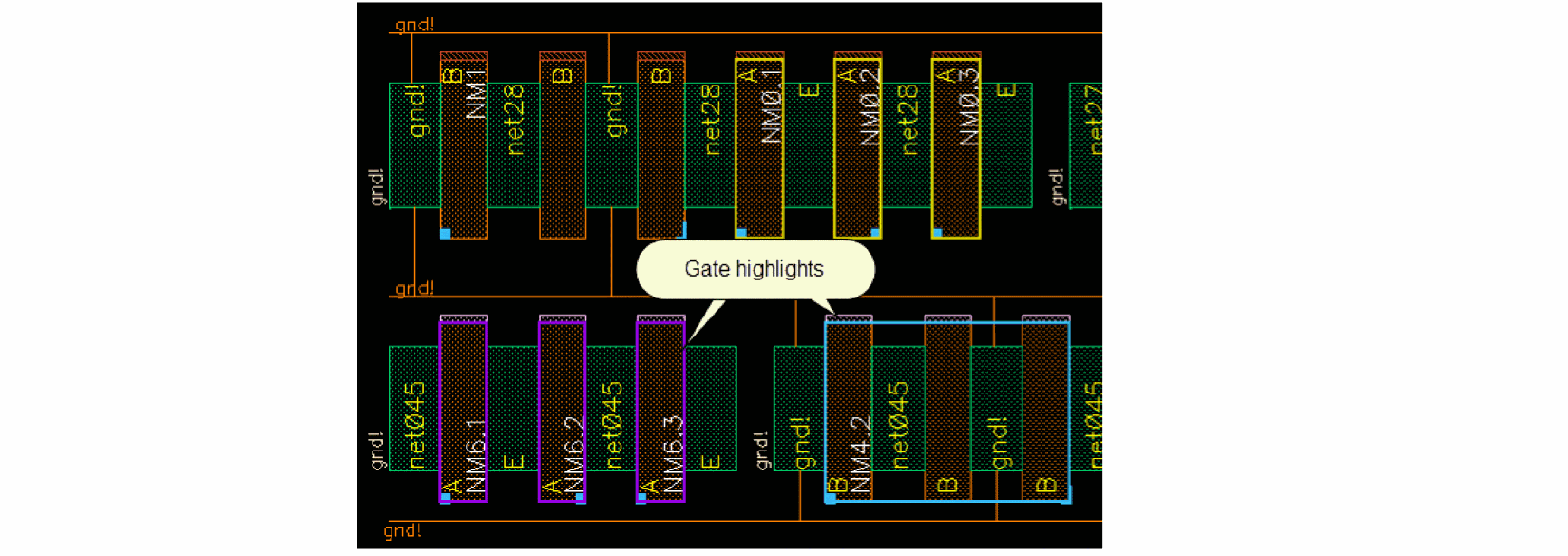
Highlight P/N device patterns on gates highlights different device patterns, such as m-factors, folds, and finger-splits in different colors in the design. This option can highlight seven patterns in the design. Gray color is reserved to highlight the indistinguishable patterns. The gate highlights are reanalyzed and updated in the canvas when:
- the Highlight P/N device patterns on gates option is enabled or disabled.
- new devices are added to the design using the Append selected from source option.
- design is reset using the Reset placement option.
- design is reopened using the Load SPD design option.
-
edit commands– Undo, Redo, Fold, Split Fingered Device, Remove, Check or Update, Stack. Unstack, and Edit Stack are used.
Environment variable: highlightGatePattern
Size for Medium Symbol sets the size for the medium symbol in the design. All other symbols, smaller and bigger, are calculated with respect to the size of the medium symbol set here.
Min Width sets the minimum width for the medium symbol.
Valid values: 0 to infinity
Environment variable: mediumSymbolMaxWidth
Max Width sets the maximum width for the medium symbol.
Valid values: 0 to infinity.
Environment variable: mediumSymbolMinWidth
Auto button for the Width option automatically calculates the minimum and maximum widths of the medium symbol.
Free specifies whether free bucket size mode should be used to display widths of symbolic devices.
Environment variable: freeSymbolWidth
Min Length sets the minimum length for the medium symbol.
Valid values: 0 to infinity
Environment variable: mediumSymbolMinLength
Max Length sets the maximum length for the medium symbol. Valid values: 0 to infinity.
Environment variable: mediumSymbolMaxLength
Auto button for the Length option automatically calculates the min and max lengths of the medium symbol.
Free specifies whether free bucket size mode should be used to display lengths of symbolic devices.
Environment variable: freeSymbolLength
If there are FinFET devices, driven by number of fins are included in the design, the Size for Medium Symbol section form displays Fins instead of Width. You can use this option to set minimum and maximum number of fins for the medium symbol.
Environment variables: mediumSymbolMinFins and mediumSymbolMaxFins
Displaying Free Bucket Size of Devices Based on Whether Horizontal Packing is Enabled
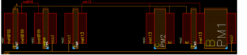
When the Options – SPD – Placement – Auto pack in X direction check box is selected, devices are packed when you choose to display free bucket size of devices. However, if this check box is deselected automatic packing of devices in the horizontal direction does not take place when free bucket size is displayed. This is shown below.
-
Devices displayed based on relative sizes. Here, PM2 is 100nm and PM1 is 200nm.
.
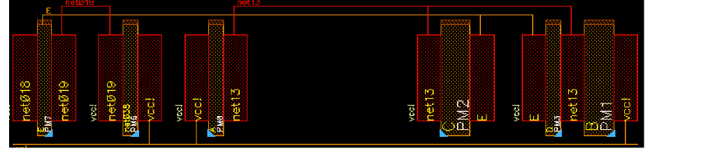
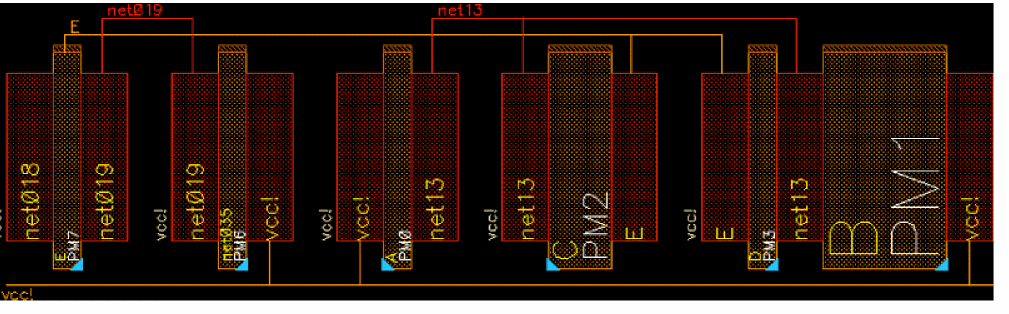
-
Devices displayed when free bucket size is enabled, but automatic packing of devices is disabled. You can see that PM1 is bigger than PM2 and devices are not packed in free bucket size mode.
-
Devices displayed when both free bucket size and automatic packing of devices are enabled. You can see that PM1 is bigger than PM2 and devices are packed in free bucket size mode.
-
Devices displayed based on relative sizes. Here, PM2 is 100nm and PM1 is 200nm.
.
Generation Options
Use the Generation options pane to configure spacing for a P-type oxide diffusion (POD) and an N-type oxide diffusion (NOD). You can also set the heights for PMOS and NMOS devices.
The Spacing section lets you set the spacing between power and ground rails with respect to POD and NOD and the spacing for between and within row-pairs. Counting from the bottom, the first and second rows are defined as a row-pair and so are the third and the fourth rows.
Power-POD specifies the spacing between a power rail and a POD.
Environment variable: spacingVddPod
Between Row-pair specifies spacing between two row pairs when generating the layout.
Environment variable: betweenRowPair
Within Row-pair specifies the spacing within a pair of rows.
Environment variable: spacingPodNod
Ground-NOD specifies the spacing between a ground rail and an NOD.
Environment variable: spacingVssNod
X: OD drop-down list specifies how oxide diffusion spacing is decided. The default value is Fixed.
Environment variable: spacingOdMode
-
Fixed specifies the oxide diffusion spacing between chains. Type a floating number in the field under the X:OD drop-down list.
Environment variable: spacingOd
-
DummyPoly specifies that the software automatically calculates the required oxide diffusion spacing between two unabutted instances. The software considers the minimum oxide diffusion spacing and the minimum poly spacing defined in the technology file and then calculates a value that satisfies both. This becomes the default setting for this option when there are FinFET devices in the design.
Environment variable: spacingOd
-
UserFunction specifies a user callback SKILL function that calculates the required oxide diffusion spacing between two unabutted instances. Enter the SKILL function name in the field under the X:OD drop-down list.
Environment variable: spacingOdUserFunc
-
Fixed specifies the oxide diffusion spacing between chains. Type a floating number in the field under the X:OD drop-down list.
Environment variable: spacingOd
For more information of dummy poly SKILL functions, see Symbolic Placement of Devices Functions in Virtuoso Layout Suite SKILL Reference.
Height sets the height of the PMOS and NMOS regions.
PMOS specifies the height for the PMOS region.
Environment variable: heightPmosRegion
PFIN specifies the height for the PFIN region. This option is available instead of PMOS, if there are FinFet devices in the design.
Environment variable: heightPmosRegion
NMOS specifies the height for the NMOS region.
Environment variable: heightNmosRegion
NFIN specifies the height for the NFIN region. This option is available instead of NMOS, if there are FinFet devices in the design.
Environment variable: heightNmosRegion
Prevent gate shorts specifies whether to prevent gate shorts across all rows when generating the layout.
Environment variable: preventGateShorts
Prevent well shorts specifies whether to prevent well shorts when generating the layout.
Environment variable: preventWellShorts
Cell (Est) displays the estimated cell height. This value is updated automatically when any of the above listed values are updated in this pane.
Click Check Fold Threshold to display the Placement pane where you can enable folding and make the fold threshold less than MOS height. This button is enabled only when either of the following is true:
The preview box on the right lets you see how spacing and height changes with each option you modify.
Power Rails Options
The Power Rails section helps you customize how power and ground rails are created in the design. Power rails can only be created for NP, PN, PNNP, and NPPN row patterns.
Create specifies whether power rails are created.
Environment variable: createPowerGroundRails
As trunk creates power rails as trunks. When selected, power rails are created as path segments and are converted to trunks. This option is available only when the Create option is selected.
Environment variable: createPGTrunk
Truncate creates power rails with no beginning and ending extension values.
Extend creates power rails with the default beginning and ending extension values.
Environment variable: pgTrunkBeginEndType
Delete existing rails specifies whether existing power rails are to be deleted when generating the layout. By default power rails are not deleted when the layout is generated.
Environment variable: deleteExistingRails
Power sets the layer, width, and net name for the power rails.
Layer specifies the layer purpose used to create the power rail for the power net.
Environment variable: layerVdd
Width specifies the width for the power rail.
Environment variable: widthVdd
Net Name specifies the net name for the power rail.
Environment variable: vddNetName
Auto Detect automatically detects the net name. This check box is selected by default. In auto mode, power nets are obtained in the following order:
- Power nets from the instances in the design.
-
The Power net names field in the Connectivity form or set using the
lxSupplyNetNamesenvironment variable. -
Default name, which is
VDD.
Ground sets the layer, width and net name for the ground rails.
Layer specifies the layer purpose used to create the power rail for the ground net. Environment variable: layerVss
Width specifies width for the ground rail. Environment variable: widthVss
Net Name specifies the net name for the ground rail. Environment variable: vssNetName
Auto Detect automatically detects the net name. This check box is selected by default. In auto mode, ground nets are obtained in the following order: - Ground nets from the instances in the design.
-
The Ground net names field in the Connectivity form or set using the
lxSupplyNetNamesenvironment variable. -
Default name, which is
VSS.
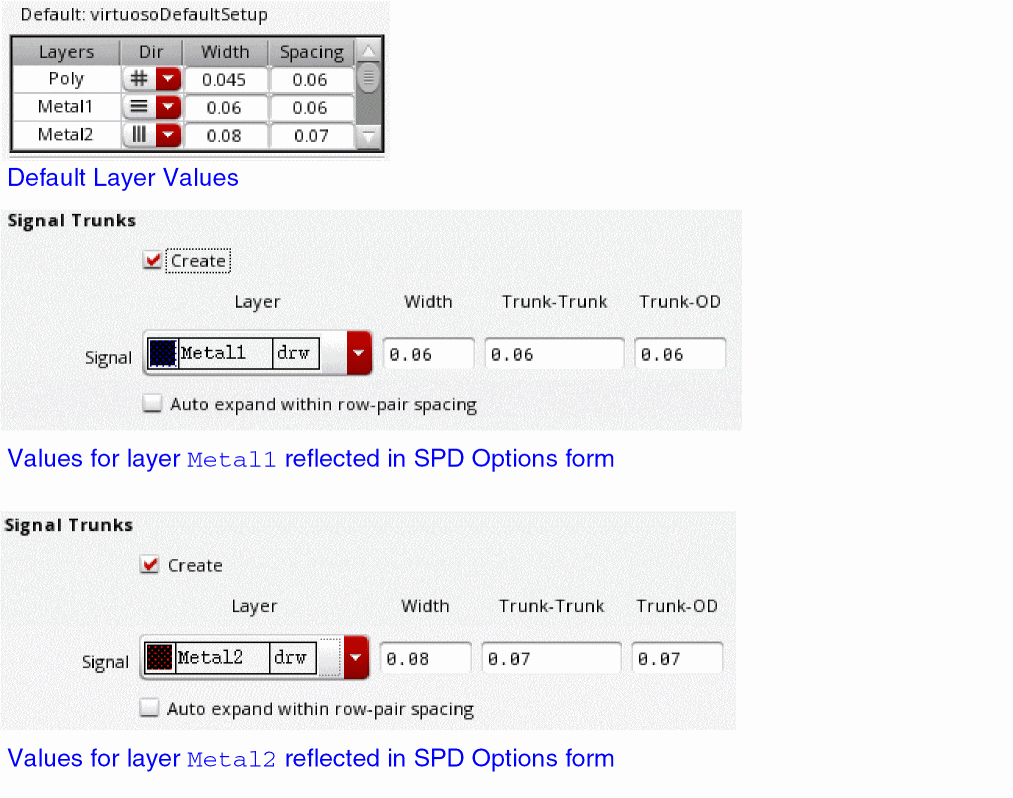
The Signal Trunks section helps you specify whether signal trunks are created when the layout is generated. You can also specify the layer purpose, width and spacing for the signal trunks.
Create specifies whether signal trunks are created
Environment variable: createSigTrunk
Layer specifies the layer purpose used to create the signal nets when generating the layout.
Environment variable: sigTrunkLr
Width specifies width for the signal net when generating the layout.
Environment variable: sigTrunkWidth
Trunk-Trunk specifies the trunk-to-trunk spacing when generating the layout.
Environment variable: sigTrunkSpacingT2T
Trunk-OD specifies the trunk-to-oxide-diffusion spacing when generating the layout.
Environment variable: sigTrunkSpacingT2O
Auto expand within row pair spacing specifies whether the maximum number of tracks need to be calculated from trunk width and spacing information including within-row-pair spacing, trunk-to-OD spacing and trunk-to-trunk spacing.
Environment variable: expandSpacingForTrunks
If you do not change the spacing and width values here, then these values are updated with the spacing and width of the corresponding layer, as shown below.
Labels Options
Use the Labels options pane to create and customize labels for the specified object type, instances, and power and ground rails.
Create labels lets you create labels in the design. By default, is not selected. All other options on this pane available only when you select the Create labels check box.
Environment variable:
Font specifies the font to be used for the labels. The default font is roman.
Environment variable:
Objects Type specifies the objects for which the labels need to be created. The options available in the drop-down list are MOS, Power/Ground Rails, and Both. The default value is MOS.
Environment variable:
For Instance customizes instance labels. These options are available only if you specify the Objects Type as MOS or Both.
Layer specifies the layer-purpose pair for the instance labels.
Environment variable: genLabelLr
Orientation sets the orientation for the instance labels.
Environment variable: genLabelOri
|
Same orientation as the instance. This is the default value. |
|
Justification sets the location of the label origin. The origin appears as a small square on the label when you place or select it. Choose from Auto, lowerLeft, centerLeft, upperLeft, lowerCenter, centerCenter, upperCenter, lowerRight, centerRight, and upperRight. By default this option is set to Auto, which sets justification as centerCenter.
Environment variable: genLabelJust
Height specifies the height of the instance label. You can choose Auto or Fixed from the drop-down list. By default, this option is set to Auto.
Environment variable: genLabelHeight
The entry field lets you manually specify the value of height for the instance labels. The default value is 0.1. This option is available only if you choose Fixed from the Height drop-down list.
Environment variable: genLabelHeightValue
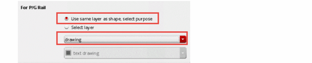
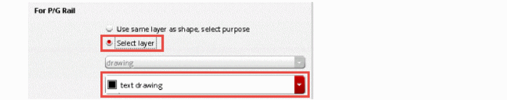
For P/G Rail customizes labels for power and ground rails. These options are available only if you choose the Objects Type in the Labels section as Power/Ground Rails or Both.
Environment variable:
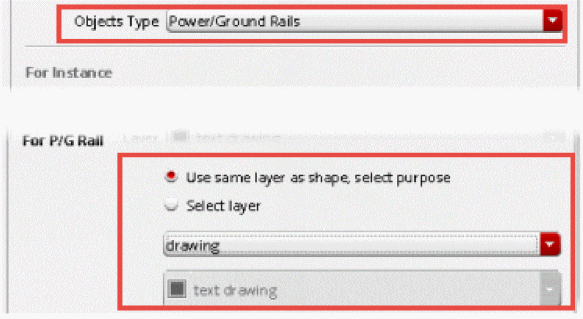
If you select the Use same layer as shape, select purpose radio button, the layer for the label is same as the shape created as the power or ground rail, which can be specified in the Power Rails Options.
You must select the purpose from the first drop-down list included in the For P/G Rail section.
Environment variable: genLabelPGPur
If you choose the Select layer radio button, you must specify both layer and purpose from the second drop-down list included in the For P/G Rail section.
Use the layer purpose drop-down list to specify the layer used to create the power rail labels.
Environment variable: genLabelPGLr
Stack Options
Use the Stack options pane to specify how you want to pack stacked devices.
The Stack Spacing options let you specify the spacing between stacked devices.
P Stacking specifies the general vertical spacing in stacked devices of P rows.
Environment variable: spacingPStack
N Stacking specifies the general vertical spacing in stacked devices of N rows.
Environment variable: spacingNStack
Max Depth specifies the limit for stacking a device. You can choose between Unlimited, No stacking, and Limited. If you choose Limited, you can specify the limit manually in the cyclic field given below. You can specify a number between 1 and 9999.
Environment variable: maxStackDepth
The preview box on the right lets you preview how stacking changes with each stacking option you modify.
Related Topics
Specifying Global Settings for Creating Stacked Devices
Setup Options
Use the Setup options pane to control how SPD is invoked.
Launch SPD in controls whether SPD starts as a tabbed window in Virtuoso Layout Suite XL or if the same window should be reused next time SPD is launched.
Tabbed window opens SPD as tabbed window in Virtuoso Layout XL. If you clear this check box, SPD opens in a separate window. By default, this option is not selected. You must close and relaunch SPD for the changes to take effect.
Environment variable: tabbedWindow
Reuse window for faster relaunch reduces time needed to restart SPD by reusing the current SPD window when the tool is restarted. By default, this option is selected.
You may want to clear this check box if:
When you change this option, you must close and reopen SPD for the changes to take effect. Environment variable: reuseWindow
Load/Save specifies the file to which you can save or load all the settings in the SPD options form.
File specifies the name of the file to be loaded or saved. By default, this file is ~/.cdsenv.
Click Save to save the option settings in the specified file.
Environment variable: optionsFile
Return to top