9
AnalogLib Components Used in RF Simulation
The Delayline Element
The delayline element is a lossless transmission line with a specified delay time Td and characteristic impedance Z0. It is intended for the small-signal ac, sp, and noise analyses, and the harmonic balance analysis and models ideal delays in these analyses.
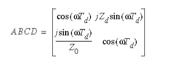
The ABCD matrix of a lossless transmission line section is given by:
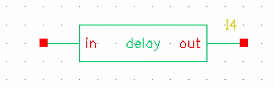
The delayline symbol is shown below.
Command-line help
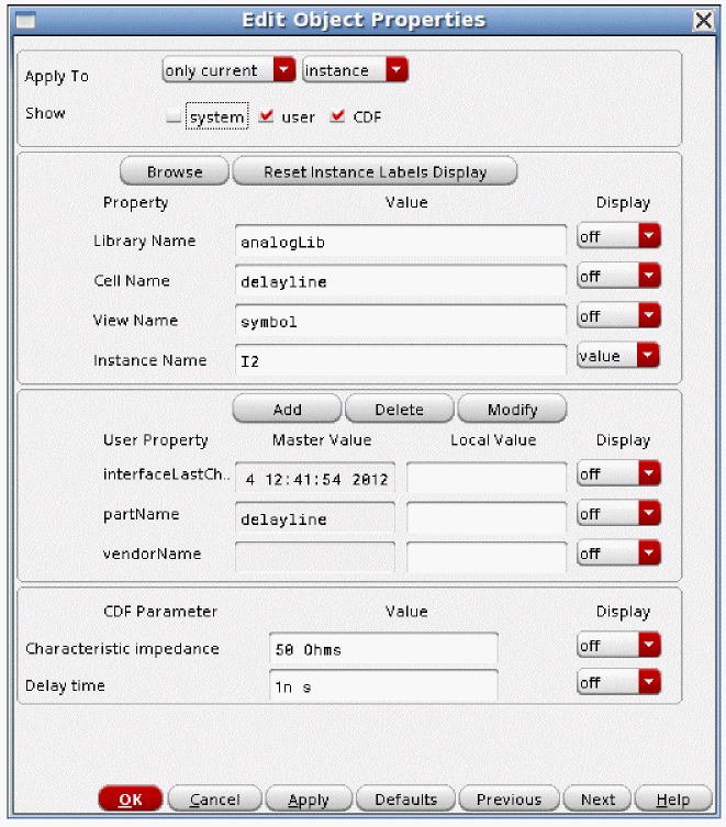
CDF Parameters
The properties list is shown below.
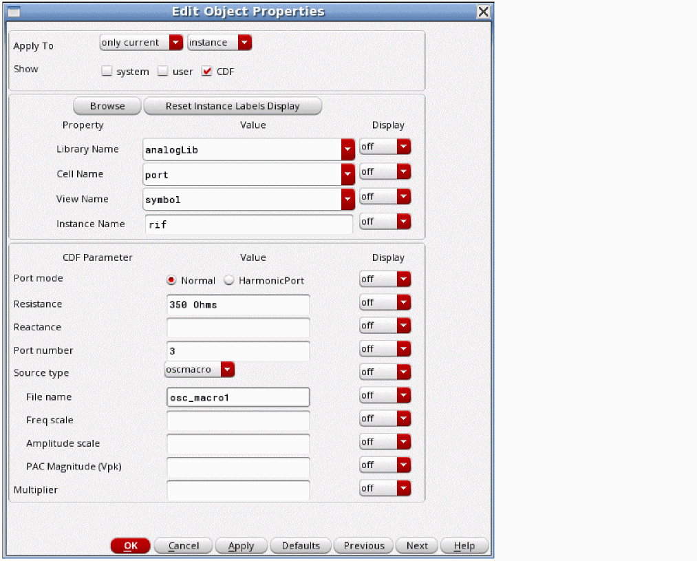
The PORT Element
You can use the port component, located in the analogLib library, in RF circuits for Spectre® circuit simulator RF Analysis (SpectreRF) and Spectre S-parameter simulations.
The port component, located in the analogLib library, is a superset of the existing psin component. The port component supports all the source types of the Spectre port primitive: pwl, pulse, sine, dc, and exp. In addition, it includes the bit and prbs source types. If you are using the psin component, it is highly recommended that you switch to the port component because the properties are organized in a better way, and the levels in volts peak and in dBm both cannot be set at the same time. This is easily accomplished by obtaining the properties form for psin, and changing the cell name to port. All the properties that are set in the psin component will retain their values when you make the change.
psin is retained for legacy designs and will not be enhanced in any way moving forward.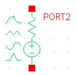
The port component is an independent resistive source tied between positive and negative terminals. It is equivalent to a voltage source in series with a resistor, where the reference resistance of the port is the value of the resistor.
Capabilities of the port Component
While the port component is most useful as a stimulus in high-frequency circuits, it also has the following unique capabilities.
- It can define the ports of a circuit to the S-parameter analysis.
- It has an intrinsic noise source that lets the noise analysis directly compute the noise figure of the circuit.
- Is the only source for which you can specify the amplitude in terms of power.
- It generates sinusoidal, exponential, piecewise-linear, periodic piecewise-linear, pulse, bit, and prbs waveforms for all the large-signal analyses.
- It can have different impedances for each harmonic number in the harmonic balance large-signal analysis.
Terminating the Port
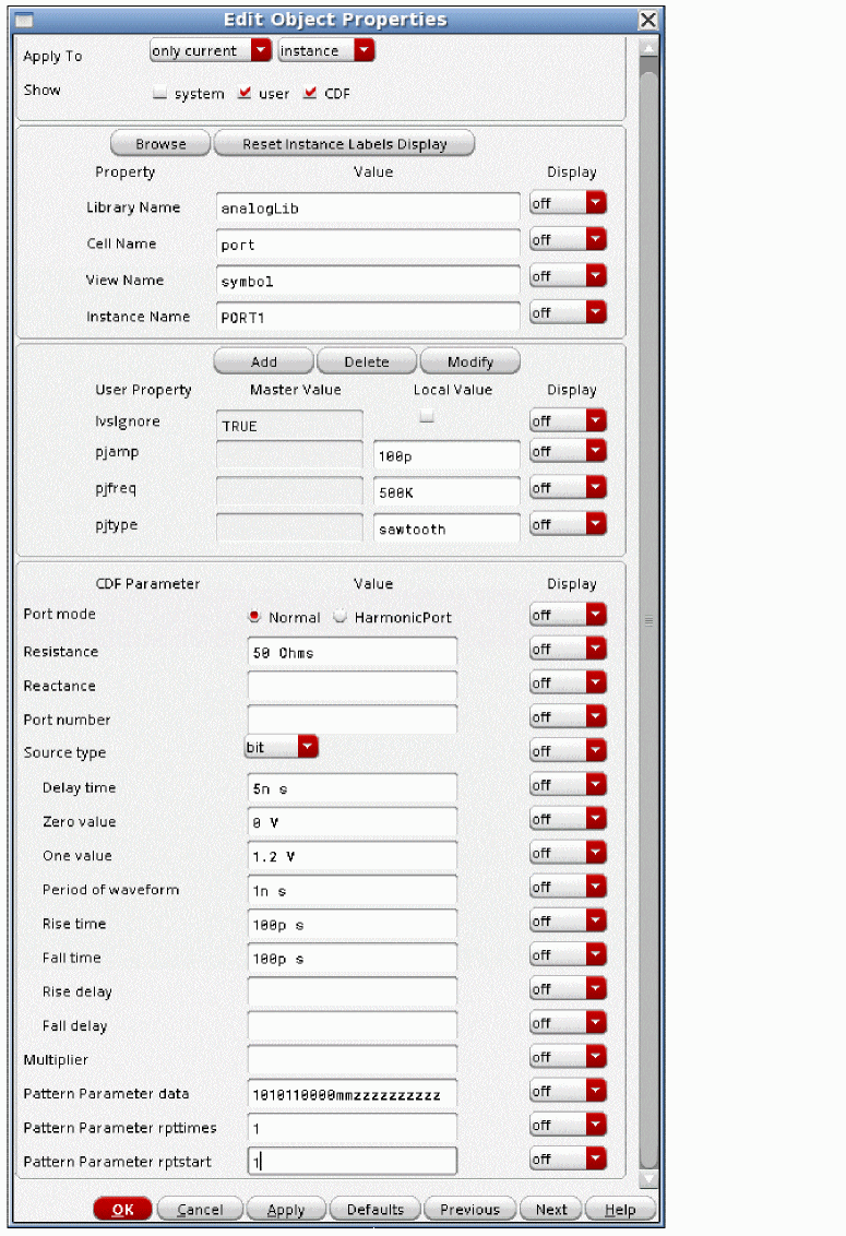
When you specify the voltage on a port, all Spectre simulations assume that the port is properly terminated in it’s reference resistance. The specified voltage value is not the voltage on the internal voltage source, which is actually set to twice the value specified on the port. If you use a port source to drive an open circuit, the voltage (for DC, transient, AC, and PAC signals) is double its specified value. However, you can alternatively specify the amplitude of the sine wave in the transient and PAC analyses as the power in dBm delivered by the port when terminated with the reference resistance. For the bit and prbs source, the voltages specified for the zero and one states are doubled inside the port as usual. For the prbs source, you can add a matching resistor across the port to get the voltages specified in the zero and one states, or you can omit the resistor, and half the desired voltages. For the bit source, if you intend to use the z state, do not add a matching resistor across the source because this small resistor will totally swamp the Z-state effect. Thus, when you use the bit source in a port, the values for the zero and one states should be half the desired voltages. This is not an issue for the vsource element.
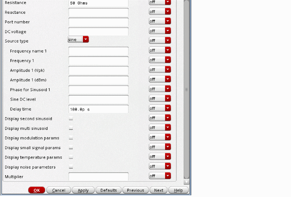
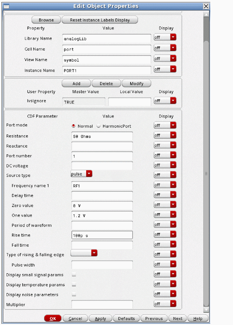
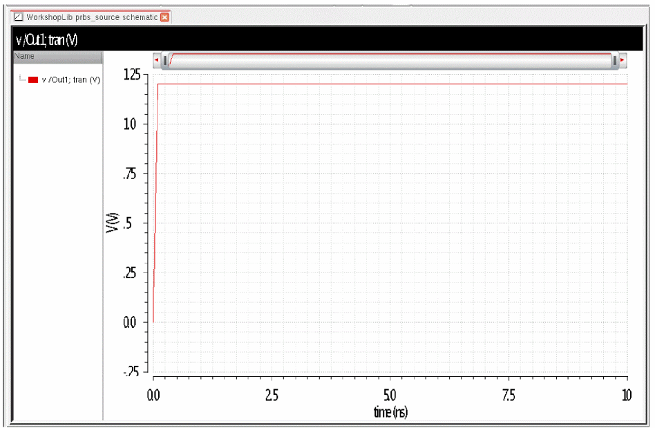
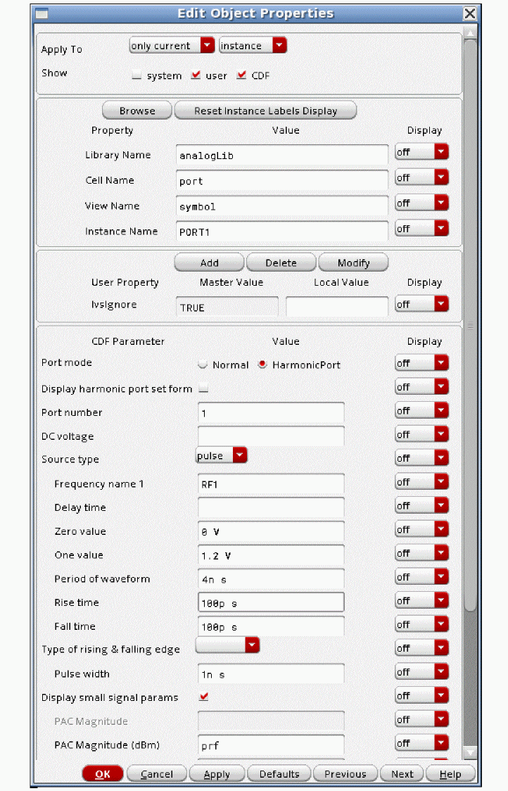
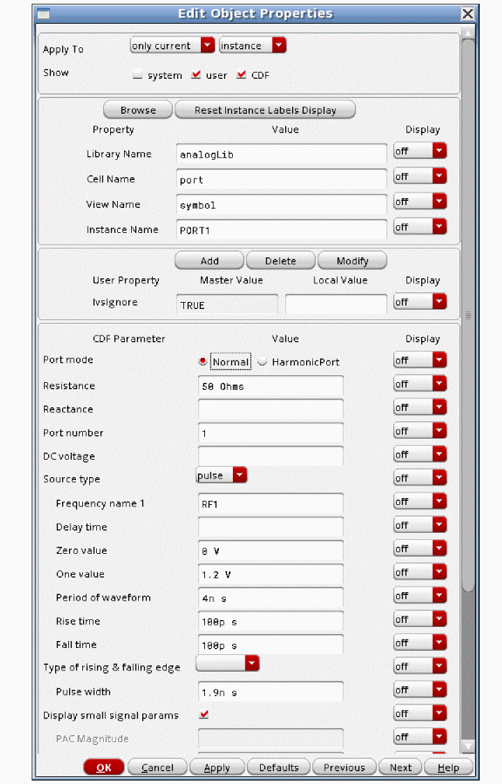
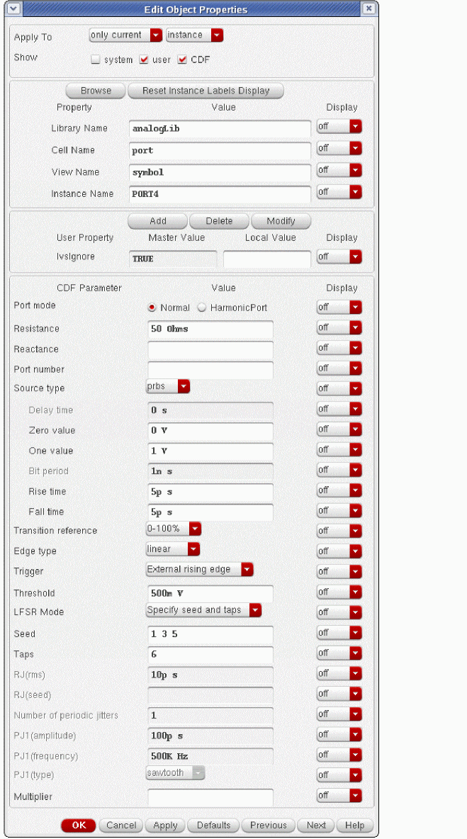
The port component Edit Object Properties form is shown in Figure 9-1 and Figure 9-2.
Figure 9-1 Top of the port Component Edit Object Properties Form
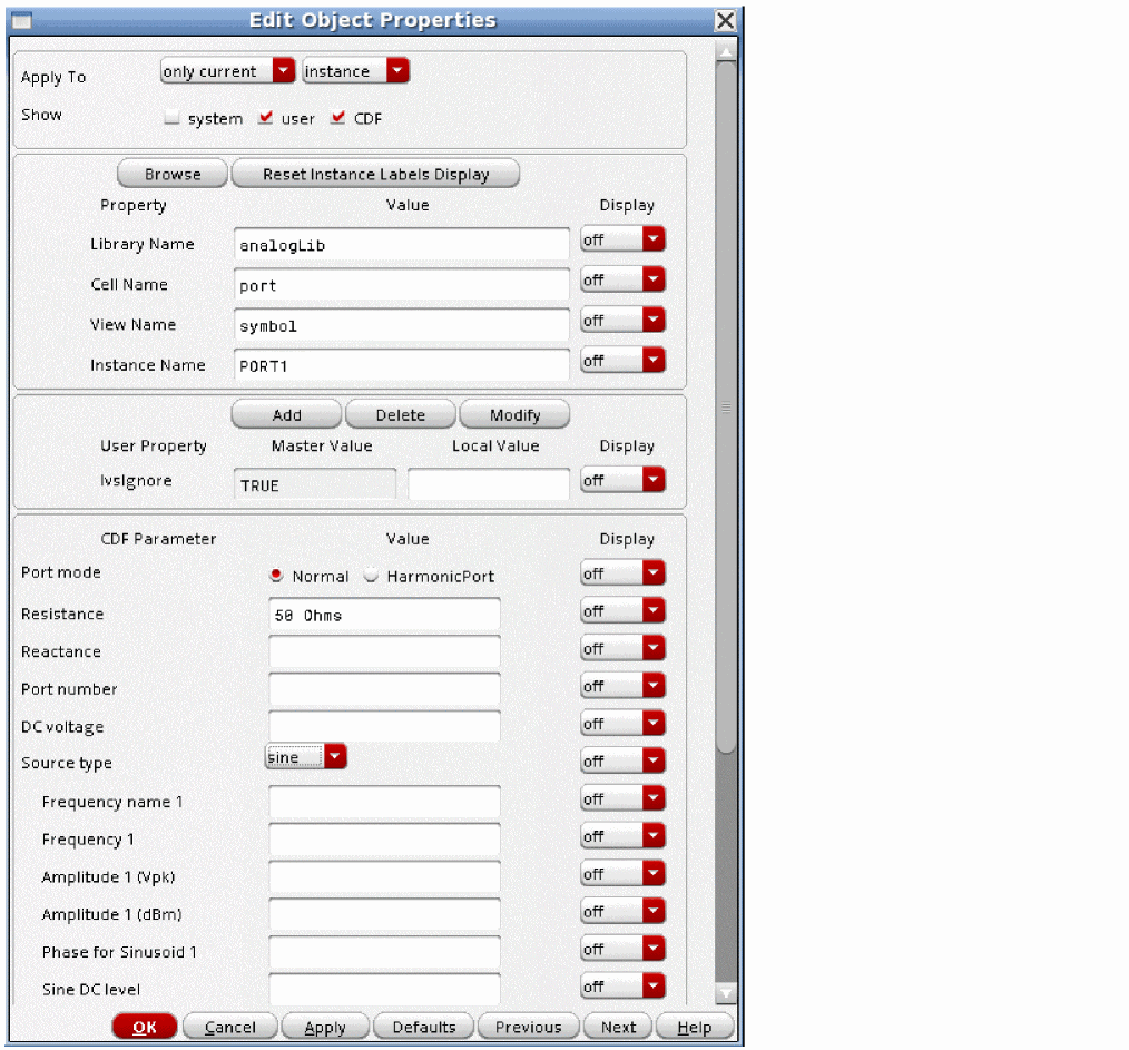
Figure 9-2 Bottom of the port Component Edit Object Properties Form
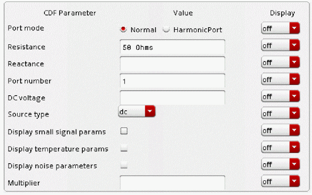
Parameters for the Port Component
Port Parameters
Port parameters include Resistance, Reactance, Port Number, and Multiplier.
Resistance
The reference resistance of the system. The value must be a real number, but not 0. The default value is 50 ohms. This applies for all analyses. Note that the resistance and reactance can be set individually for each harmonic in harmonic balance large-signal analyses only. For more information, refer to Using the Harmonic Port with Harmonic Balance.
Reactance
The imaginary part of impedance is used for harmonic balance large and small-signal analyses, and for the ac, noise, xf, sens, stb, pz, and sp.analyses. The reactance is not used for the dc, transient, and shooting-based large and small-signal analyses. The value must be a real number. The default is zero ohms. Note that the resistance and reactance can be set individually for each harmonic in harmonic balance large-signal analyses only. For more information, refer to Using the Harmonic Port with Harmonic Balance.
Port number
The number associated with the port. The value must be a non-zero integer and must be unique for each port in a schematic. The port number is not automatically indexed when you place a new port on your schematic. There is no need to assign this number because in the sp analysis, you just select the port instances you want from the schematic.
If you do assign port numbers, start with the number one, and number the ports sequentially. A gap in the port number sequence causes a simulation error if the port list is not defined in the S-parameter analyses.
Leave this property at the default. The multiplicity factor specifies the number of ports in parallel. The value must be a non-zero real number and the default is 1. For example, if you set Resistance to 50 and Multiplier to 2, you specify two ports in parallel, with an effective reference resistance of 25 ohms.
Using the Harmonic Port with Harmonic Balance
The port component has a feature called harmonic port that allows the specification of different impedances at different harmonic numbers. This is available for harmonic balance large-signal analyses only and does not work with any other analysis.
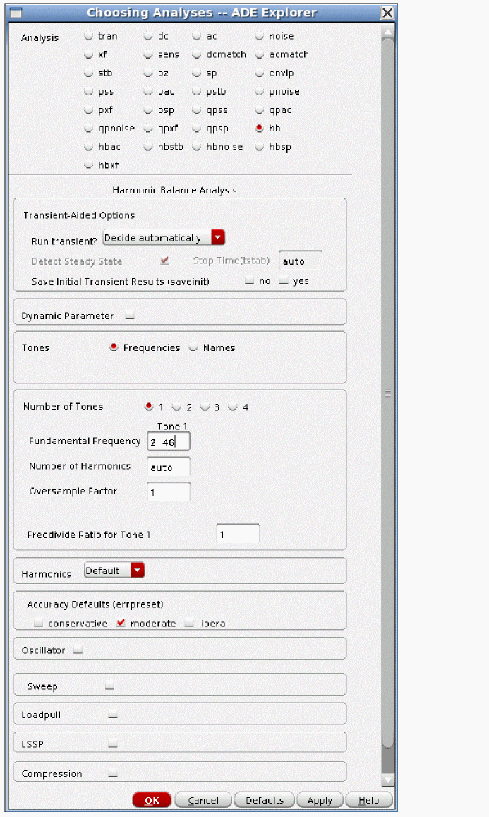
For this example, a 2.4GHz LNA is the example circuit.
The input and output ports are set up normally, as shown in the properties forms below.
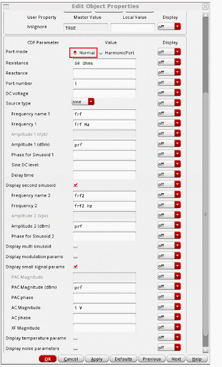
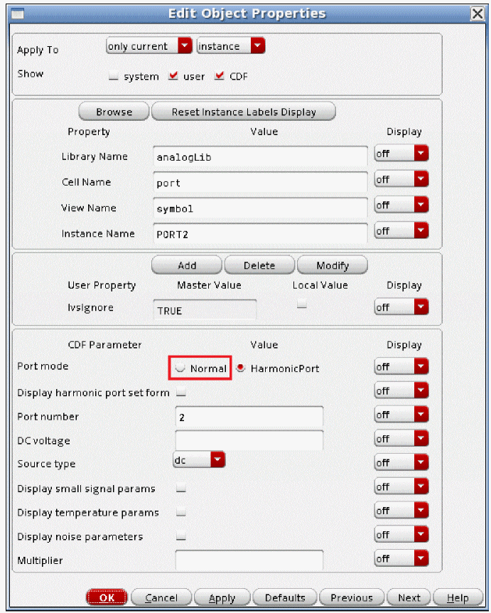
PORT1 is the input and PORT2 is the output.
One Input Frequency
The harmonic balance Choosing Analyses form has a single input applied.
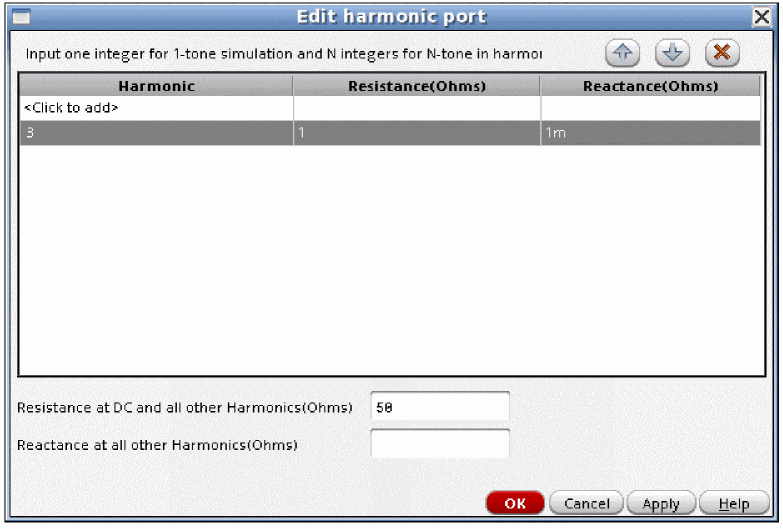
To use the harmonic port, select Harmonic Port on the properties form. In this case, the port being used as a load in the circuit is selected. The Edit harmonic port window is displayed.
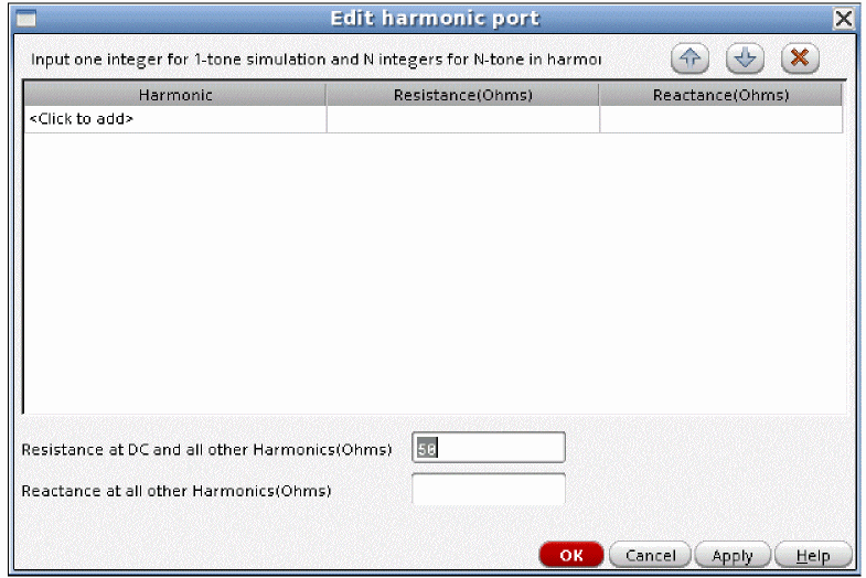
For this setup, a single input frequency is applied to the circuit. In this case, harmonic numbers 1, 2, 3, 4, and 5 exist in the simulation result. In the Harmonic column, you enter the harmonic number. In the Resistance column, you enter the resistance. In the Reactance column, you enter the series reactance in ohms. Positive reactance adds inductance, and negative reactance adds capacitance. Multiple entries are allowed, so different impedances can be set for each harmonic. The resistance or reactance can be left blank, which is interpreted as zero resistance or reactance.
- Double-click on the last variable in the variables list. The Editing Design Variables window is displayed.
- In the Editing Design Variables window, click Next. The Name and Value (expr) fields become editable.
- Enter the variable name in the Name field, and the starting value in the Value (expr) field.
- Click OK or Apply. The variable and value are entered into the table.
ERROR: Length of hvec is not equal to length of rvec multilies tones or length of rvec is not equal to length of xvec.
Here is a comparison where the third harmonic is set normally in the top trace, and to 1 ohm in series with +j1mohm in the bottom trace. The lower impedance for the third harmonic in the bottom trace lowers the amplitude of the third harmonic.
Two Input Frequencies
Now the harmonic balance Choosing Analyses form has two frequencies.
Also, the diamond cut is set with a very large MaximOrder. The reason for doing this is to see the harmonic numbers that correspond to the frequencies produced by the circuit. Each frequency has two harmonic numbers that indicate which harmonics are mixing with which to produce a specific output frequency. For example, take the 2.44GHz term. The harmonic number is 1 0. The frequency that is produced is 1*2.44G + 0*2.46G. Now look at the intermod at 2.42GHz. This index is 2 -1. The frequency is 2*2.44G - 1*2.46G. These are the harmonic numbers that can be set for the harmonic port. Wild cards (*) are not allowed in the harmonic number specification.
Note that if there were three input frequencies, there would be three numbers that specify every output frequency.
In this case, if the harmonic was specified as 3, there would be an error produced by Spectre because there is a single index in the harmonic, but there are 2 indices for all the harmonics of the existing simulation. The number of entries in the Harmonic field must match the number of input frequencies in the circuit.
The above example sets the impedance of the third-order intermods to be much lower than 50 ohms. If the source is in series, setting the resistance and/or reactance to a large number can block harmonics you don’t want. If the port is in parallel like this one, setting small resistance and reactance values can short out an undesired harmonic. This can be used for debugging the circuit, or for setting values to maximize power-added efficiency. The resistance or reactance can be left blank, which is interpreted as zero resistance or reactance.
The top trace above is from the normal port, and the bottom trace is from the harmonic port. The third order harmonics are much smaller because they are essentially shorted out.
Source type
The Source type parameter lets you select a wave shape for the port from the Source type cyclic field: dc, pulse, exp, pwl, pwlz, sine, bit, prbs, oscmacro, or blank. Each Source type has different parameter settings associated with it. You can define several different wave shapes and quickly switch between them without losing the wave shape settings. The wave shape settings are described in detail in the following sections:
- DC Parameters
- Pulse Waveform Parameters
- PWL Waveform Parameters
- Sinusoidal Waveform Parameters
- Exponential Waveform Parameters,
- Bit Waveform Parameters,
- PRBS Waveform Parameters
The typical Source types used in SpectreRF analyses are: dc, piecewise linear, pulsed, and sine. For example, you can quickly switch from a sinusoid (for PSS analysis) to a DC level (for PAC analysis) by changing the Source type from sine to dc. The sinusoidal properties remain with the port, and can be changed when the Source type is returned to sine. This is true when switching between any of the sourcetypes. All the properties are retained for everything that you define.
When you set Source type to a blank value, the port acts as a resistive load.
DC Parameters
To generate a dc level from the port component, select dc in the Source type cyclic field. When the Source type is set to dc, the dc
The dc setting sets the DC level for all analyses.
DC voltage
The DC voltage parameter sets the port’s DC level for all analysis. The value must be a real number. If you do not specify the DC value, the default value is 0 volts.
The DC voltage parameter specifies the DC voltage across the port when it is terminated in its reference resistance. In other words, the DC voltage of the internal voltage source is double the specified DC value, dc. Because all small signal analyses (AC, SP, XF, and Noise) use DC
Figure 9-3 Source type=dc in the Edit Object Properties form
The Display small signal params, Display temperature params, and Display noise parameters fields are discussed in Small-Signal Parameters, “Temperature Effect Parameters”, and “PRBS Waveform Parameters”.
Pulse Waveform Parameters
The pulse waveform can generate a step, a single pulse, or a periodic pulse waveform.
To generate a pulse waveform from the port component, select pulse in the Source type cyclic field.
When you specify the voltage on a port, you are specifying the voltage when the port is properly terminated, and not the voltage on the internal voltage source. Therefore, the voltage on the internal source is set to twice the value specified on the port.
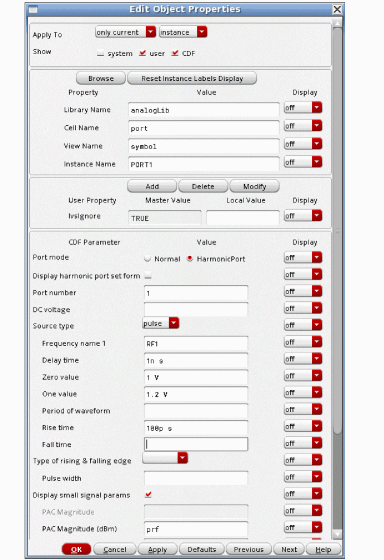
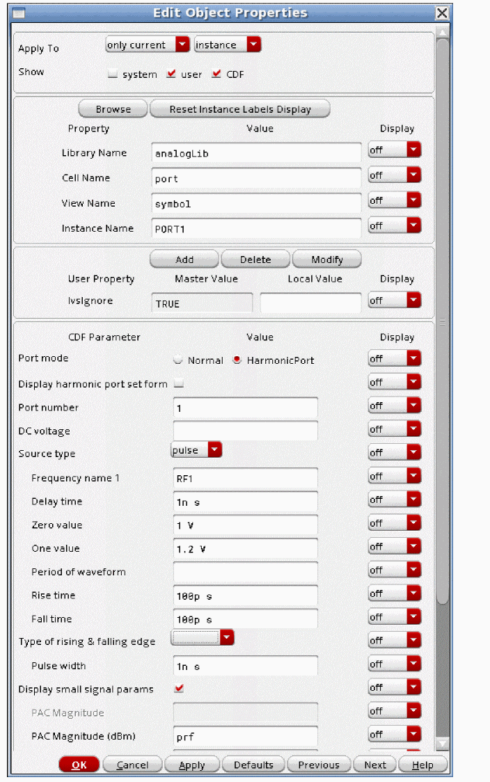
Figure 9-4 Source type=pulse in the Edit Object Properties form
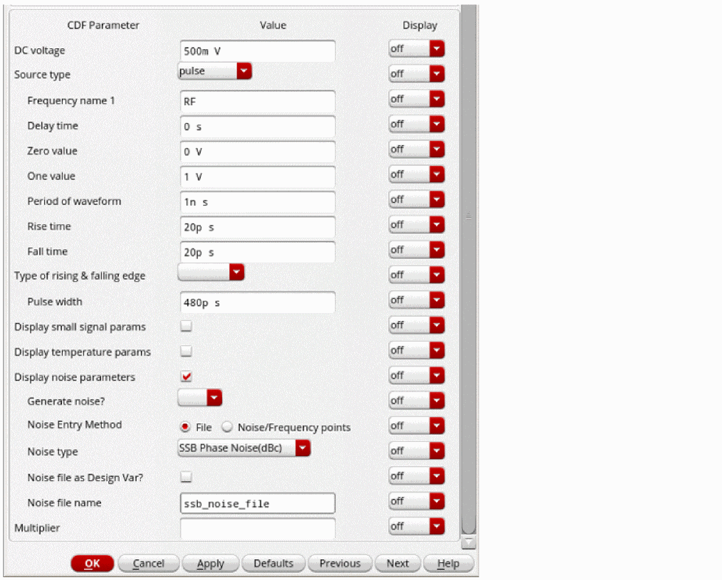
Frequency name 1
The Frequency name 1 parameter is listed in the Fundamental Tones section of the Choosing Analyses form for pss, qpss, and hb when Names is selected.
Delay time
The Delay time parameter is the simulation time that the port stays at the zero value without becoming periodic. Generally, this should be set less than the period of the waveform. Longer times are allowed, however, this forces a transient analysis until the longest delay time before the large-signal analyses pss, qpss, and hb can start. If a 1GHz signal and a delay time of 1 second is in your circuit, a transient is forced for 1 billion cycles of the input before the pss, qpss, or hb can start. This effectively prevents them from starting because of the long simulation time in the transient analysis. This must be a real number.
Zero value
The Zero value property is the time-zero value of the pulse in Volts. The default is zero volts.
One value
The One value property specifies the voltage that the signal transitions to at time equals zero plus. The default is one volt, which is unlikely to be what you want. Always set this property.
Period of waveform
The period property specifies the period of the pulse. If this property is left blank, a single pulse is generated at the beginning of the transient simulation.
Rise time
The Rise time property specifies the zero to 100% risetime for the pulse. This is the time for the complete transition from the zero value to the one value.
Fall time
The Fall time property specifies the zero to 100% falltime for the pulse. This is the time for the complete transition from the one value to the zero value.
Pulse width
The Pulse width property specifies the time to remain at the one value. The default is infinity.
Pulse Waveform Examples
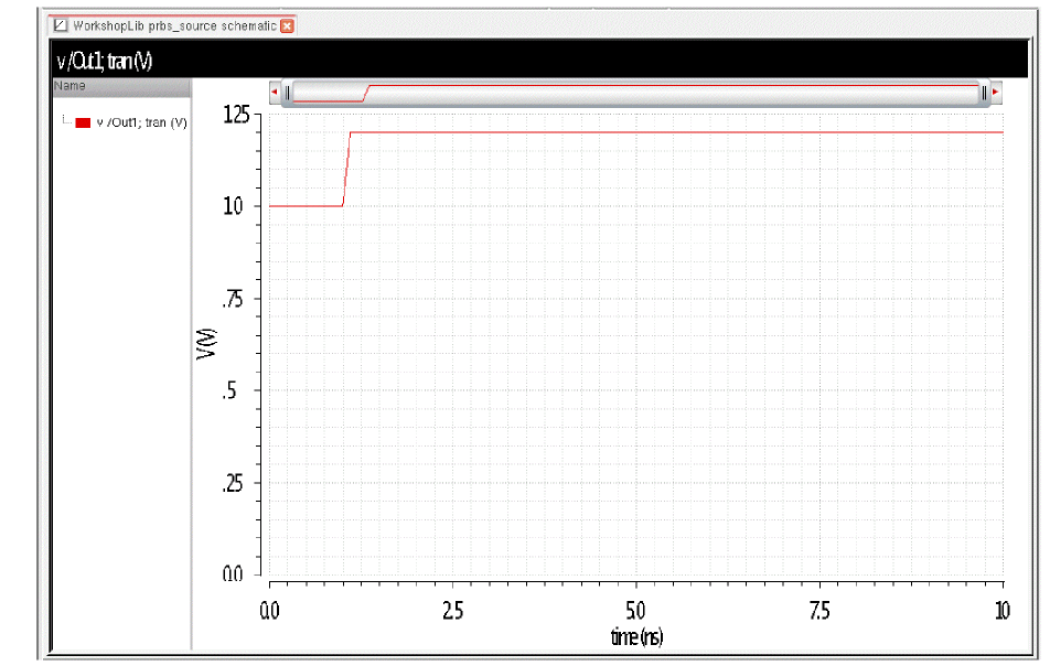
Generating a step from zero to 1.2 Volts
- Set the Zero value field to 0 volts.
- Set the One value field to 1.2 volts.
-
Set the risetime to a time that is appropriate for your circuit. A suggested starting value is about
 .
.
The default is the falltime. If the falltime is not given, the default is . If the period is not given, then the default is
 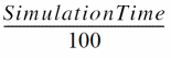 .
.
The waveform is shown below.
-
Setting a Delay time to 1n shifts the waveform to the right.
The waveform is shown below.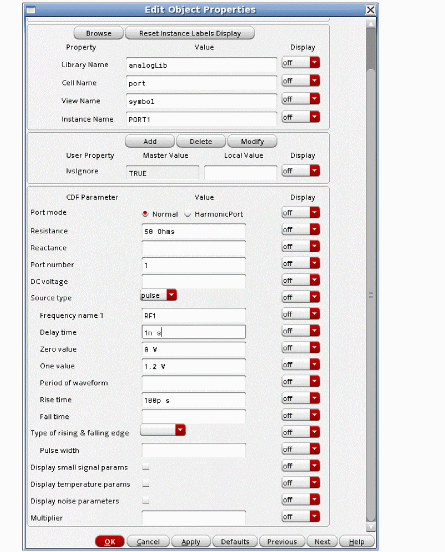
Specifying a startup bump in a supply voltage
This is commonly used to start oscillators, and is usually done using a vsource.
- Set the Zero value to about 80% of the supply voltage.
- Set the One value to the supply voltage.
-
Set the Rise time as appropriate for the system you are simulating.
-
The waveform is shown below.
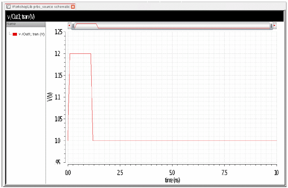
Specifying a single pulse at startup, then zero after that.
This is usually used with the ipulse or isource components to start an oscillator.
- Set the Zero value to zero.
- Set the One value large enough to get things started.
- Set the rise and fall times to about one tenth of the period of the oscillator.
- Set the Pulse width to about three tenths of the period.
- Leave the Period of waveform field blank.
-
The waveform is shown below.
To generate a pulse with an arbitrary duty cycle and differing rise and fall times:
- Set the Zero value and One value fields to the levels needed for your system.
- Set the Rise time and Fall time fields to approximate the real input source. The values can be different.
- Set the Period of waveform field to the value needed for your frequency.
-
Set the Pulse width between 0.05 to about 0.95 times the period.
-
The waveform is shown below.
To generate a 50% duty cycle square wave:
- Set the Zero value and One value fields as appropriate for your system.
- Set the Rise time and Fall time fields as appropriate for your system and make them equal.
- Set the Period of waveform field to that needed to generate your input frequency.
-
Set the Pulse width to half the period minus the risetime.
-
The waveform is shown below.
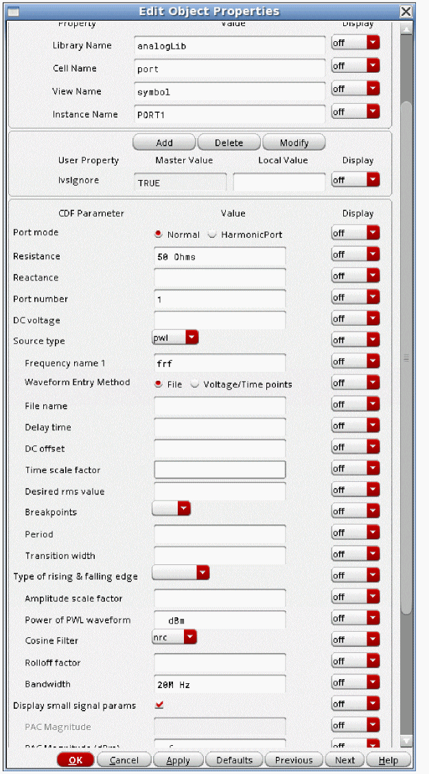
PWL Waveform Parameters
Piecewise linear waveforms allow an arbitrary input waveform to be generated. The input can either be a file that contains time and voltage pairs, or you can enter the time-voltage pairs directly in the PWL source properties form. Remember that the voltages you enter in the piecewise linear file assume that the port is properly terminated. The internal voltage source gets set to double the value specified in the piecewise linear voltage specifications.
To generate a piecewise linear waveform from the port component, select pwl in the Source type cyclic field. This sets the Source type CDF parameter to pwl and displays additional fields for the PWL CDF parameter settings.
When you specify the voltage on a port, you are specifying the voltage when the port is properly terminated, and not the voltage on the internal voltage source. Therefore, the voltage on the internal source is set to twice the value specified on the port.
Figure 9-5 Source type=pwl in the Edit Object Properties form
Waveform Entry Method
With the Waveform Entry Method buttons, select how you enter piecewise-linear data,
- By specifying a File name.
- By entering a series of Voltage/Time points directly in the properties list for the port.
File name
When you select File as the Waveform Entry Method, type the name of the file containing your piece wise-linear data in the File name field. The file name must be a string. There is no default. In ADE Explorer, define the directory that contains the file by selecting Setup - Simulation Files, and entering either the rooted path (starts with slash (/)) or relative path (starts with dot (.)) in the Include Paths field. Multiple directories can be specified in the Include Paths fields.
In your file, list the piecewise-linear data in the form of time-value pairs. Enter one pair per line with a space or tab between the time and voltage values. The numbers in the file must use exponential notation, for example, 1.04e-3. You can also use SI scale factors (p, n, u, m, k, M, G, etc.).
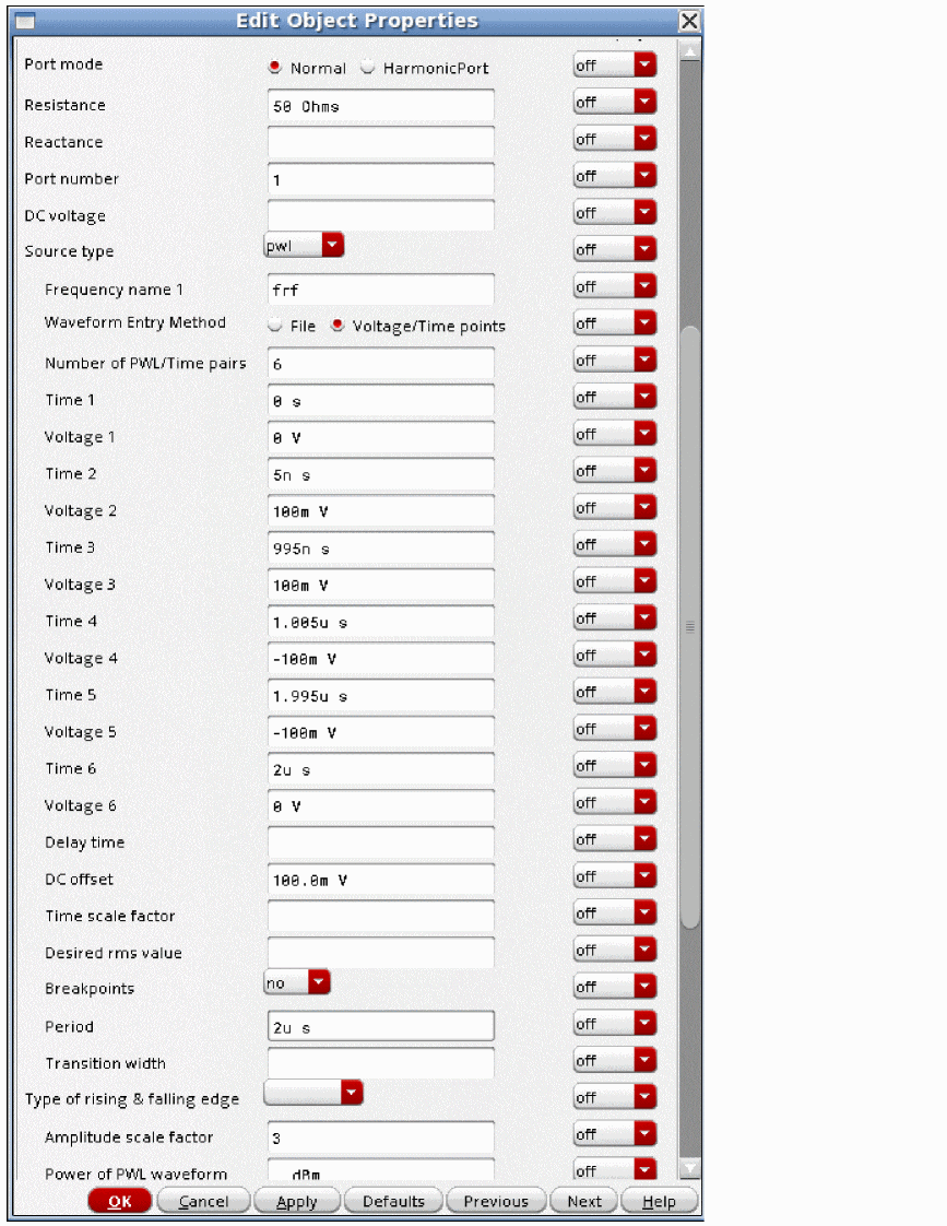
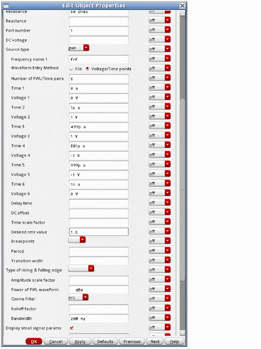
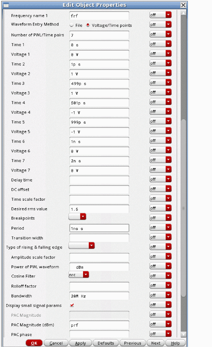
Number of PWL/Time pairs
When you select Voltage/Time points as the Waveform Entry Method, the Number of PWL-Time pairs field (tvpairs) form opens. Enter the number of time-value pairs you plan to enter. The form expands to let you enter the designated number of Time
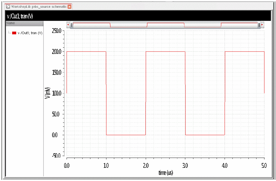
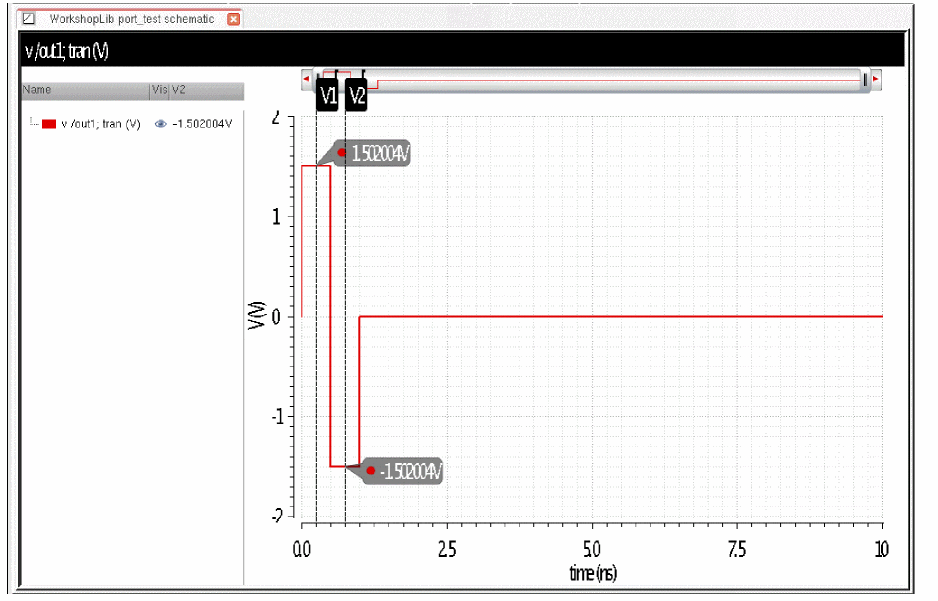
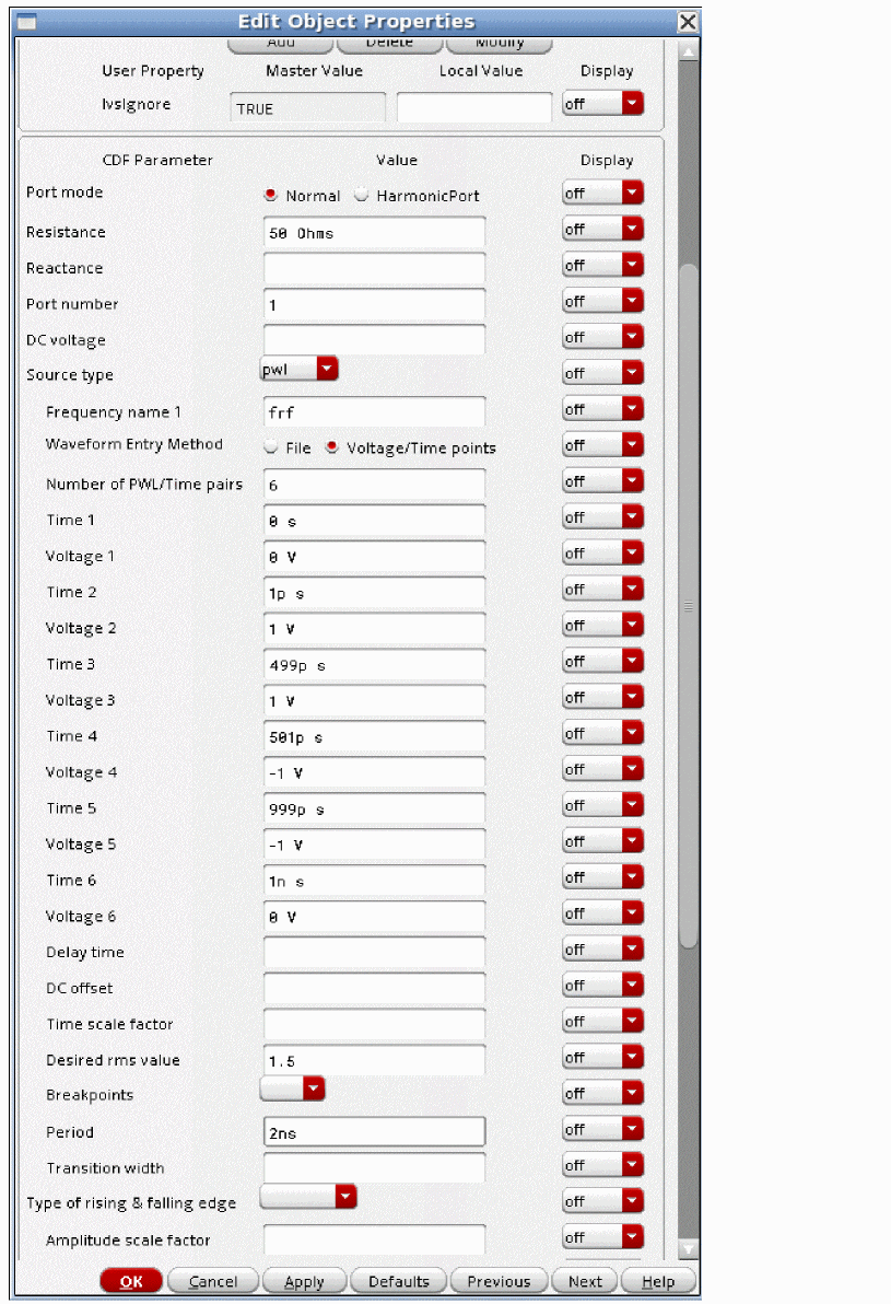
In this example, the number of voltage-time pairs is 6.
Figure 9-6 Waveform Entry Method=Voltage/Time points
The waveform that is produced is shown below.
The DC offset, Amplitude scale factor, and Time scale factor parameter fields let you quickly adjust the amplitude, frequency, and offset of your piecewise-linear data pairs without editing each individual time-value pair in the PWL waveform.
DC offset
DC offset for the PWL waveform. The default is zero volts.
To show the effect of setting both the DC voltage and DC offset properties, in the following example, the DC Voltage and the DC offset are both set to 0.1.
Note that the signal only observes the DC offset in the transient.
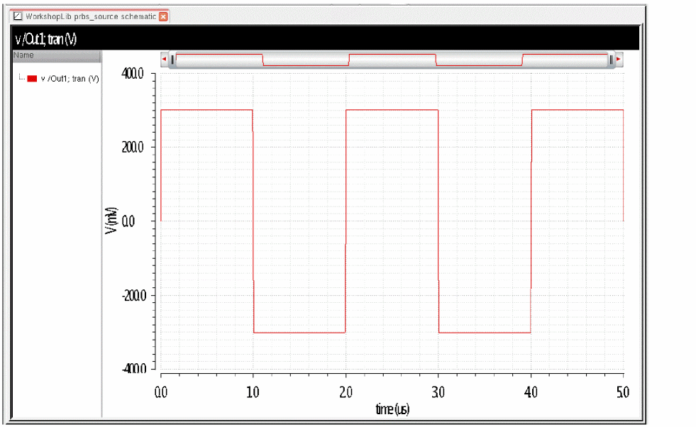
Amplitude scale factor
Amplitude scale factor (scale) for the PWL waveform. The default value is 1. The example below shows a scale factor of 3.
Note that the waveform is multiplied by three in amplitude.
Time scale factor
Time scale factor is a multiplier for the times given for PWL waveform. Default is 1. Setting the time scale factor greater than 1 increases the times in the file, and reduces the frequency.
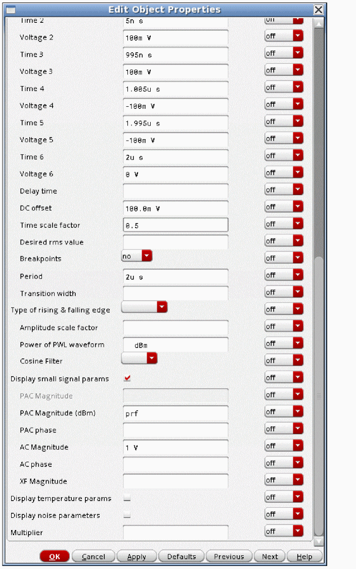
Note that setting the time scale factor to 0.5 multiplies all the times including the time in the period property.
Cosine Filter
The raised cosine filter is used when the PWL source is used to define digital modulation. Values are none (default), and nrc. nrc specifies a raised cosine filter to be used on the output waveform of the PWL source. This can be used to lower the numerical noise floor of the modulation specified in the I and Q modulating file. When nrc is selected, the PWL file must have evenly spaced points with timepoints at 1/(2*Bandwidth of the filter).
Rolloff factor
When nrc is selected, the Rolloff factor (rolloff) of the filter can be specified. The default value is 0.2, which is reasonable for simulations. If you consider a continuous waveform, changing the rolloff factor has an effect on the ringing that is produced in the time domain. Smaller rolloff factors produce more ringing in the continuous waveform. Envelope does not simulate the continuous waveform. Instead, envelope samples the waveform at the time interval in the I and Q modulation file. This delta-time in the I and Q file is always related to the modulation frequency, and it also determines the bandwidth of the cosine filter as described below. The effect of this is that the sampling occurs at the times where the ringing of the filter is zero. Therefore, the cosine filter does not change the spectral content calculated in envelope. It just reduces the numerical noise floor of the input signal.
Bandwidth
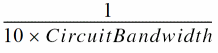
The Bandwidth (pwlbandwidth) of the Cosine Filter. If you want to only allow in-band modulation, this is the channel bandwidth. If you want to allow an accurate ACPR measurement, set the bandwidth to three times the channel bandwidth. If you want to measure two adjacent channels for ACPR, set the bandwidth to five times the channel bandwidth. Note that the I and Q data must have properly spaced time intervals of ![]() for this capability to be used.
for this capability to be used.
nrc is selected in the Cosine Filter drop-down list.Desired rms value
Desired rms voltage for the PWL waveform. Note that this will be set based on the datapoints in the PWL file or in the manually defined points entered directly into the properties form only. This has implications for periodic piecewise linear or if you go beyond the last point in the file in the transient analysis.
If the signal is defined for only part of the period or if you go beyond the last point in the pwl description, the rms calculation will not take into account the fact that the signal remains at the last voltage after the last timepoint in the pwl file. If you want this to be taken into account, define a point in the pwl description at the stop time of the transient or at the end of the period.
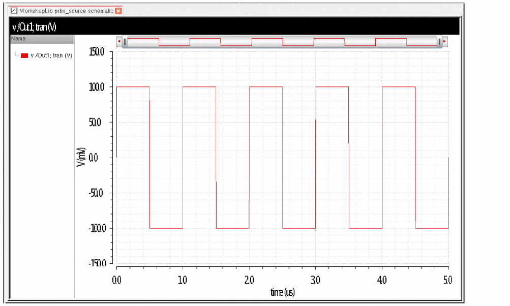
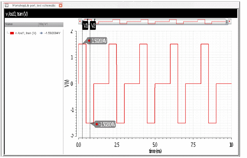
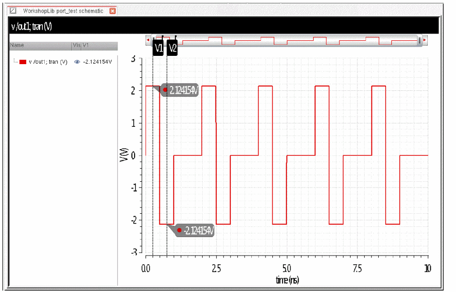
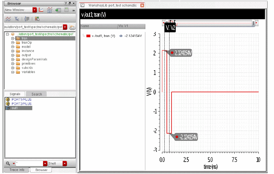
Consider an example in which a 1GHz signal is being generated, with points for the first period of 1GHz defined. No points after 1nsec exist in the PWL description. Also note that the desired RMS value is set to 1.5 (volts).
Now the transient result is plotted.
Vertical markers have been placed at the midpoint of the high and low states. The voltage is slightly greater than 1.5 because of the finite rise and fall times in the PWL description.
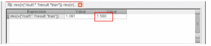
Now, the period is set to 2nsec. This will make the waveform periodic at 500MHz.
Now the transient result is plotted. Note that the high and low values are the same as before.
Now the transient waveform is sent to the calculator, and the actual rms value is calculated.
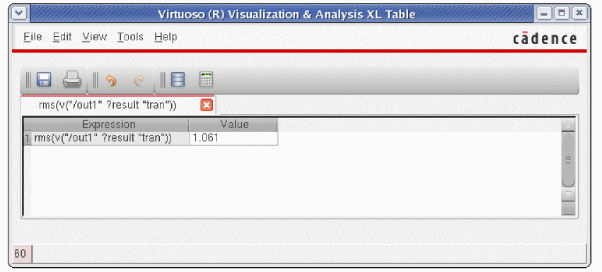
Instead of producing 1.5 volts as specified, only 1.061 volts is produced.
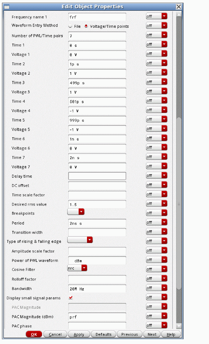
Now add another datapoint in the PWL description at 2nsec, and zero volts. Now the period and the time interval that defines the PWL points exactly agree.
Now the transient result is plotted.
Note that the positive and negative voltages have changed. This is because the PWL description completely defines the waveform during the entire first period of the waveform.
Now the signal is set to the calculator, and the rms is calculated. It is appended to the last table.
Now the RMS value is exactly 1.5 volts.
Now leave the last timepoint at 2nsec, and reduce the period to 1nsec.
Now, the transient result is plotted. The positive and negative voltages still reflect the rms value for the 2nsec interval defined by the timepoints themselves. It has not truncated the timepoints to just the first period. It is also not periodic. When the period is smaller than the time of the last timepoint in the PWL description, Spectre assumes that the period is in error, and ignores the property.
Do not set Desired rms value and Power of PWL waveform at the same time. If both are specified, first the amplitude is calculated based on the Power of PWL waveform property, and then that amplitude is multiplied by the Desired rms value setting.
Delay time
The Delay time parameter sets the time that the signal remains at the first point in the file before the pwl points begin to take effect. Generally, this should be set less than the period of the waveform. Longer times are allowed, however, this forces a transient analysis until the longest delay time before the periodic large-signal analyses pss, qpss, and hb can start. If a 1GHz signal and a delay time of 1 second is in your circuit, a transient is forced for 1 billion cycles of the input before the pss, qpss, or hb can start. This effectively prevents them from starting because of the long simulation time in the transient analysis.
Breakpoints
Possible values are no, yes, or blank. If you set Breakpoints to yes, you force SpectreRF to place time points at each point specified in a PWL waveform during a transient analysis. This can be very expensive for waveforms with many points. If you set Breakpoints to no, SpectreRF inspects the waveform, looking for abrupt changes, and forces time points only at those changes. If you set Source type = pwl and set Breakpoints to blank, the default is yes if the number of points you specify is less than 20.
Period
The PWL waveform is periodic if you specify Period in seconds.
If the value of the waveform you specify is not exactly the same at both its beginning and its end, then you must provide a non-zero value for Transition Width.
Power of PWL waveform
This is the power in dBm for a 50 ohm resistor for the output of the PWL source. See Desired rms value for important information about how to define timepoints in the PWL input points. Do not set Desired rms value and Power of PWL waveform at the same time. If both are specified, first the amplitude is calculated based on the Power of PWL waveform property, and then that amplitude is multiplied by the Desired rms value setting.
Transition Width
Transition width (twidth) is used when making PWL waveforms periodic and the ending value of the PWL file does not equal the beginning value. The default is the PWL period/1000.
Before repeating, the waveform changes linearly in an interval of Transition Width from its value at (Period – Transition Width) to its value at the beginning of the waveform. Thus, the Transition Width must always be much less than the Period.
Sinusoidal Waveform Parameters
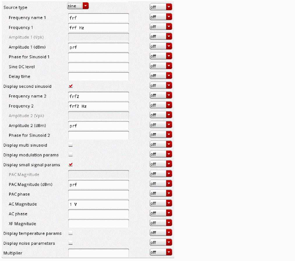
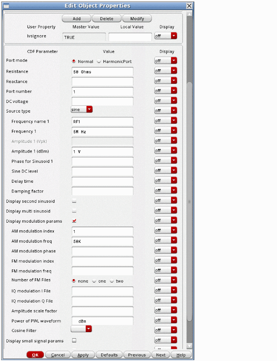
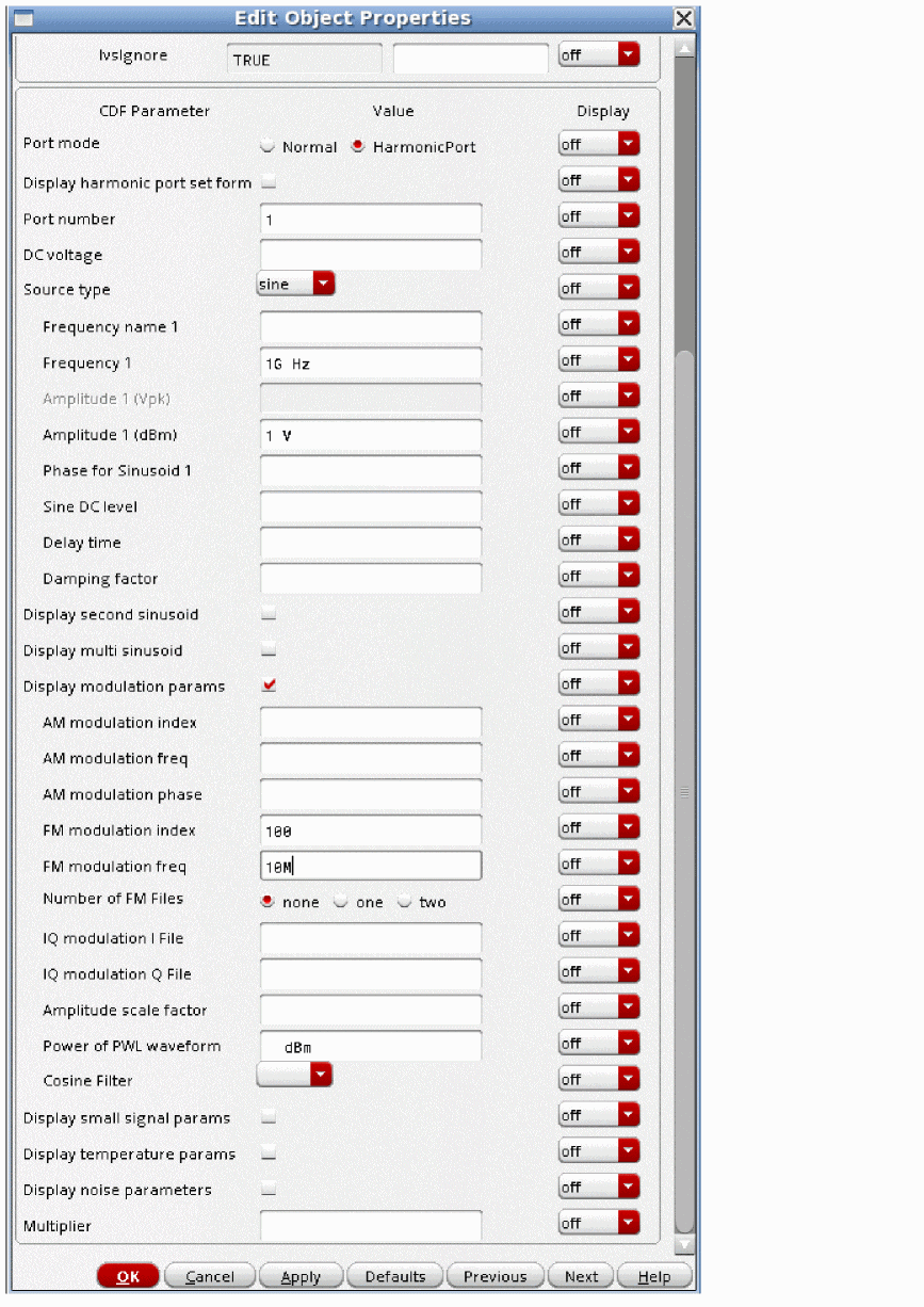
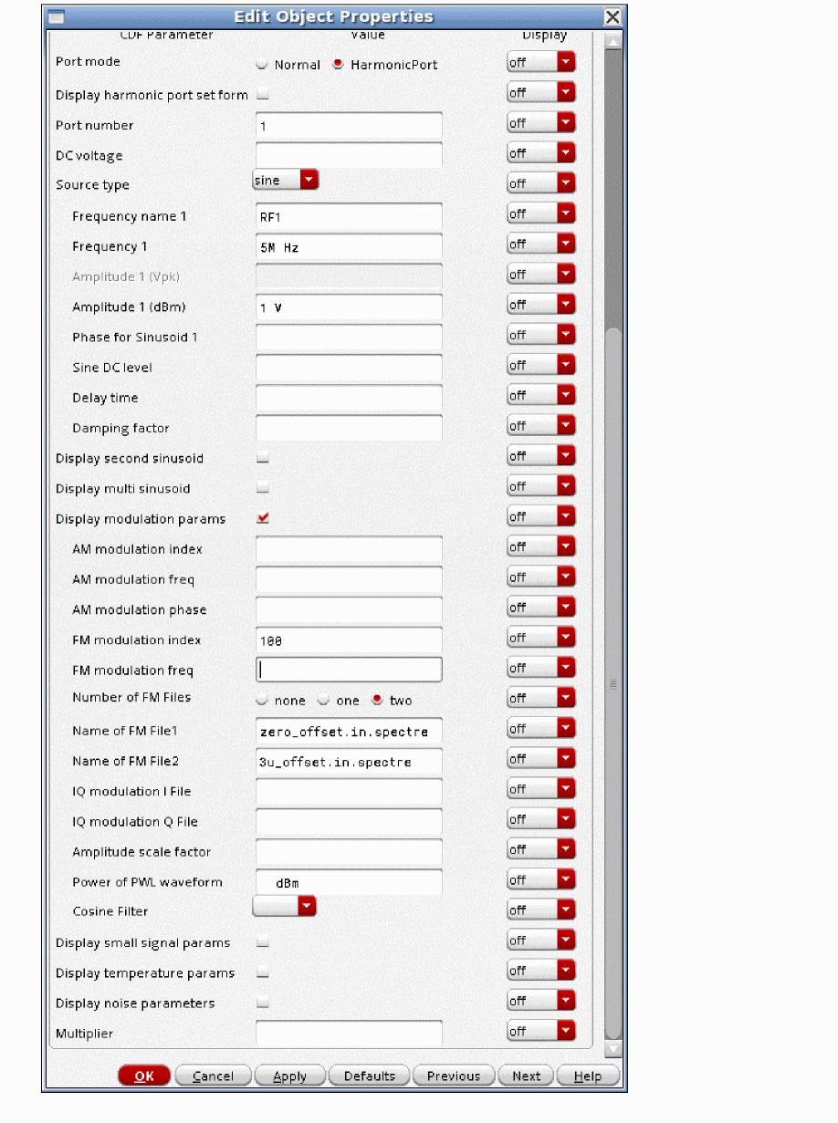
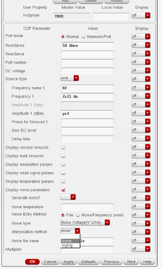
The port component can generate up to two sinusoids simultaneously. They are denoted as 1 and 2. You can set the amplitude, frequency, and phase for both individually. The amplitude can be set to either a voltage or a power level. When you set a power level, the assumption is that the port is perfectly matched. The source that is internal to the port gets double the amplitude specified by the power in dBm.You can also specify sinusoidal AM or FM modulation of sinusoid 1. Sinusoid 2 cannot be modulated.
To generate sinusoidal waveforms, set the Source type in the properties list to sine.
The first sinusoid is described by the parameters Frequency name 1, Frequency 1, Amplitude 1 (Vpk), Amplitude 1 (dBm), Phase for Sinusoid 1, Sine DC level, and by AM or FM modulation terms.
Figure 9-7 Source type=sine in the Edit Object Properties form
Frequency name 1
This property names the fundamental tones of sinusoid 1. After you save the schematic, the names you assign appear in the Fundamental Tones list box on the Choosing Analyses form.
Frequency 1 is the
Amplitude 1 (Vpk)
The peak amplitude of the first sinusoidal waveform that you generate. The value specified is the voltage delivered into a matched load. You can select either Amplitude 1 (Vpk) or Amplitude 1 (dBm), but not both. If Amplitude 1 (Vpk) has a value, the Amplitude 1 (dBm) field is grayed out. The value must be a real number. The default is 1 volt.
When you specify the voltage on a port, you are specifying the voltage when the port is properly terminated, and not the voltage on the internal voltage source. Thus, the voltage on the internal source is set to twice the value specified on the port.
Amplitude 1 (dBm)
Amplitude 1 (dBm) is the amplitude of the first sinusoidal waveform, in dBm.The resistance for the dBm calculation is taken from the resistance of the port. The value specified is the power delivered into a matched load. You can select either Amplitude 1 (Vpk) or Amplitude 1 (dBm), but not both. If Amplitude 1 (dBm) has a value, the Amplitude 1 (Vpk) field is grayed out. The value must be a real number.
Phase for Sinusoid 1
The phase at the specified Delay time. To achieve a specified phase and still remain continuous, the sinusoidal waveform might start before the given Delay time. For example, if you want to generate a cosine wave, set this parameter to 90
Sine DC level
Sets the DC level in volts for sinusoidal waveforms in large-signal analyses. This parameter is used when the sinusoid has a different average level than the one specified for the DC analyses. If not specified, the average value of the sinusoid is the same as that of the DC level of the source.
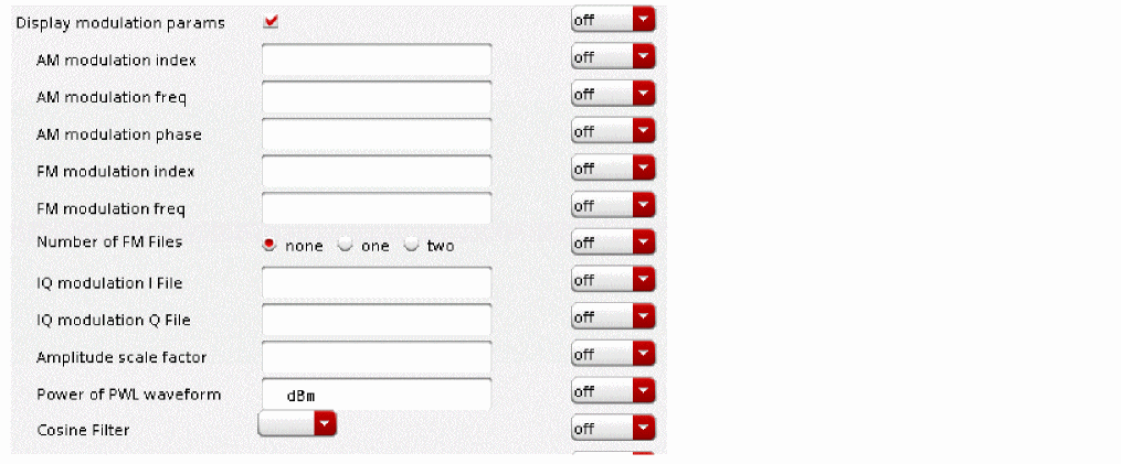
Modulation Parameters
Display Modulation Parameters
When selected, the form expands and the following modulation parameters are displayed: FM modulation index, FM modulation freq, AM modulation index, AM modulation freq, AM modulation phase, and Damping factor.
Figure 9-8 Display modulation params
AM Modulation (Background Information)
The amplitude modulation for the sinusoidal case is defined as
-
 is the amplitude modulation waveform
 -
 is the carrier frequency
 -
 is the AM modulation index
 -
 is the modulation frequency
 -
 is the AM modulation phase
The amplitude modulation parameters affect only the first sinusoid generated by port. They have no effect on the second sinusoid.
AM modulation Index
This property specifies the amplitude of the modulation signal. When the AM modulation index is 1.0, the signal is 100% modulated. When the AM modulation index is 0.5, the signal is 50% modulated.
AM Modulation Frequency
This property specifies the frequency of the sine wave that is used to modulate the signal that is specified in the Frequency 1 property. The AM modulation frequency should be much lower than the Frequency1 property.
AM Modulation Phase
This specifies the initial phase of the AM modulation sinusoid. The default is zero degrees.
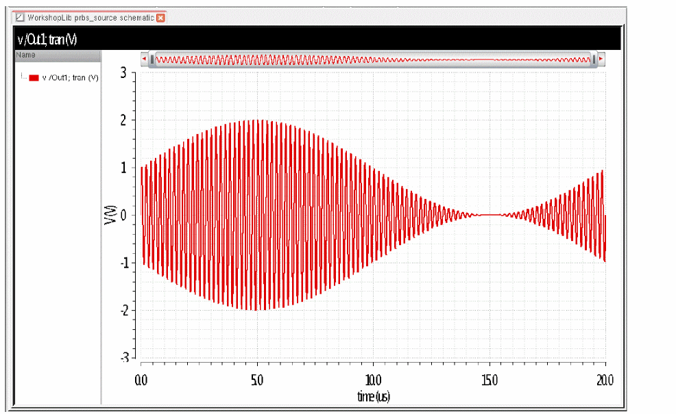
The Edit Object Properties form for a 100% modulated signal is shown below.
The output waveform is shown below.
FM Modulation (Background Information)
The frequency modulation for the sinusoidal case is defined as:
V
- A is the amplitude of sinusoid 1
- β is the FM modulation index
-
sin(2πf
m t) is the modulation signal -
f
c is the carrier frequency - φ is the phase for sinusoid 1
The frequency modulation parameters affect only the first sinusoid generated by port. They have no effect on the second sinusoid.
FM modulation frequency
FM modulation frequency for the sinusoidal waveform (f
FM modulation index
FM index of modulation for the sinusoidal waveform. It is the ratio of the peak frequency deviation divided by the modulation frequency (β in the above equations).
When the modulation index is 1.0, the deviation frequency from the carrier frequency is equal to the modulation frequency.
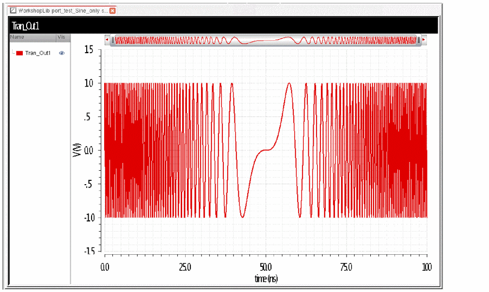
The property list for an FM signal with a modulation index of 100% is show below.
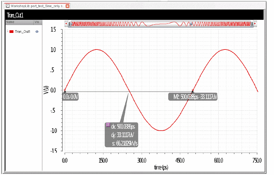
The transient waveform goes from zero frequency to twice the center frequency. This is an extremely large modulation index. Zero frequency is produced at the center of the below waveform.
When zoomed in near the beginning, the frequency is nearly double the carrier frequency.
Number of FM Files
The first sinusoid can also be phase modulated with a pair of PWL files that define the desired modulation.
-
none specifies that the FM signal should be modulated with a sinusoid.
In this case, the FM signal from the source will be represented as:
VFM (t) = A sin(2πfct + β sin(2πf m t)) -
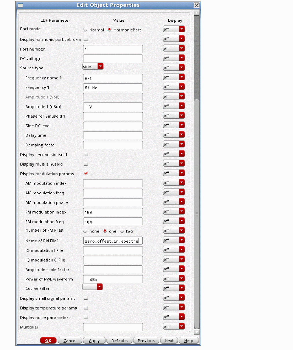
When one is selected, a Name of FM File1 field appears. Provide the filename of the PWL file that is to be used for the frequency modulation.
In this case, the FM signal from the source will be represented as:
This is shown in the Edit Object Properties form, as shown below.
-
When two is selected, the Name of FM File1 and Name of FM file2 fields appear. Provide the filename of the PWL file that is to be used for the phase modulation.
In this case, the FM signal from the source will be represented as:
Here,
 is the frequency modulation index
where
I(t)is the waveform specified in the Name of FM File1 pwl file, andQ(t)is
waveform specified in the Name of FM File2 pwl file. This is shown below.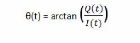
Modulating a carrier with a digital modulation I and Q file
This capability provides exactly the same capability as the ACPR_Source in rfLib. The I and Q PWL files provide the information to be modulated, and the source acts as an ideal modulator.
IQ modulation I File
This parameter should be set to the filename to the PWL file that contains the digital modulation ‘I’ information. This is a file with two columns. The left column is the time, and the right column is the voltage. Usually, the file is generated with a constant delta-T from entry to entry in the file. Generally, this file is provided by the system designer.
IQ modulation Q File
This parameter should be set to the filename to the PWL file that contains the digital modulation ‘Q’ information.This is a file with two columns. The left column is the time, and the right column is the voltage. Usually, the file is generated with a constant delta-T from entry to entry in the file. Generally, this file is provided by the system designer.
Cosine Filter
The raised cosine filter is used when the PWL source is used to define digital modulation. Values are none (default), and nrc. nrc specifies a raised cosine filter to be used on the output waveform of the PWL source. This can be used to lower the numerical noise floor of the modulation specified in the I and Q modulating file. When nrc is selected, the PWL file must have evenly spaced points with timepoints at 1/(2*Bandwidth of the filter).
Rolloff factor
When nrc is selected, the Rolloff factor (rolloff) of the filter can be specified. The default value is 0.2, which is reasonable for simulations. If you consider a continuous waveform, changing the rolloff factor has an effect on the ringing that is produced in the time domain. Smaller rolloff factors produce more ringing in the continuous waveform. Envelope does not simulate the continuous waveform. Instead, envelope samples the waveform at the time interval in the I and Q modulation file. This delta-Time in the I and Q file is always related to the modulation frequency, and it also determines the bandwidth of the cosine filter as described below. The effect of this is that the sampling occurs at the times where the ringing of the filter is zero, thus the cosine filter does not change the spectral content calculated in envelope. It just reduces the numerical noise floor of the input signal.
Bandwidth
The Bandwidth (pwlbandwidth) of the Cosine Filter. If you want to only allow in-band modulation, this is the channel bandwidth. If you want to allow an accurate ACPR measurement, set the bandwidth to three times the channel bandwidth. If you want to measure two adjacent channels for ACPR, set the bandwidth to five times the channel bandwidth. Note that the I and Q data must have properly spaced time intervals of ![]() for this capability to be used.
for this capability to be used.
nrc is selected in the Cosine Filter drop-down list box.
The Rolloff factor and Bandwidth options are available only when nrc is selected in the Cosine Filter.
Damping factor
This property is available in the vsin and isin components only.
Damping factor
v(t) = A e−σt sin(2πft + φ)
-
If
σ = 0, the waveform is a pure sinusoid (steady state). -
If
σ < 0, the waveform exhibits growing amplitude. -
If
σ > 0, the waveform exhibits decaying amplitude. - The value must be a real number. The default is 0 and the unit is 1/seconds.
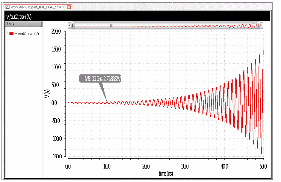
For the vsin component, am example property list is shown below.
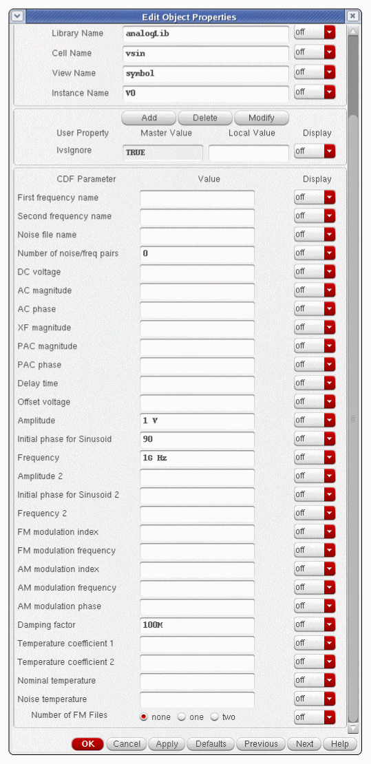
The amplitude is 1 volt. The initial phase of 90 degrees starts the sine wave at a peak so that the amplitude at 1/100M seconds or 10nsec will be at a peak that can be measured with a marker in the waveform tool. The transient analysis has strobeperiod set so a datapoint at exactly 10nSec is produced in the output. With a positive damping factor, the waveform decays, and the amplitude is 1/e at 10nsec.
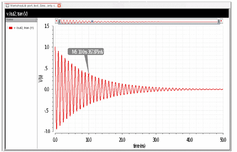
When the damping factor is negative, the amplitude is e (2.7182...) at 10 nsec.
Display second sinusoid
Displays the CDF parameters for the second sinusoid in the Edit Object Properties and Add Instance forms. When selected, the form expands to show the following CDF parameters: Frequency name 2, Frequency 2, Amplitude 2 (Vpk), Amplitude 2 (dBm), and Phase for Sinusoid 2.
Figure 9-9 Display second sinusoid
Frequency name 2
Name for the second sinusoid. After you save the schematic, the name you assign is listed in the Fundamental Tones section of the Choosing Analyses form for pss, qpss, and hb when names is selected.
Frequency 2 is the frequency of the second sinusoidal waveform in Hertz. There is no default value.
Amplitude 2 (Vpk)
Peak amplitude of the second sinusoidal waveform. The value specified is the voltage delivered into a matched load. You can select either Amplitude 2 (Vpk) or Amplitude 2 (dBm), but not both. If Amplitude 2 (Vpk) has a value, the Amplitude 2 (dBm) field is grayed out. The value must be a real number. The default is 1 volt.
When you specify the voltage on a port, you are specifying the voltage when the port is properly terminated, and not the voltage on the internal voltage source. Thus, the voltage on the internal source is set to twice the value specified on the port.
Amplitude 2 (dBm)
Amplitude 2 (dBm) is the amplitude of the second sinusoidal waveform, in dBm. The resistance for the dBm calculation is taken from the resistance parameter of the port. the value specified is the power delivered into a matched load. You can select either Amplitude 2 (Vpk) or Amplitude 2 (dBm), but not both. If Amplitude 2 (dBm) has a value, the Amplitude 2 (Vpk) field is grayed out. The value must be a real number. Units: dBm
Phase for Sinusoid 2
The phase at the specified Delay time for the second sinusoid. To achieve specified phase while still remaining continuous, the sinusoidal waveform might start before the given Delay time. The value must be a real number. Default: 0 Units: degrees.
Display multi sinusoid
Multi sinusoid is a way of generating up to nine unmodulated signals at the same time from the port component. It works in all the large-signal analyses, and is usually used with harmonic balance or qpss-harmonic balance for the simulation of systems with multiple carriers.
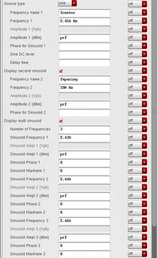
When Display multi sinusoid is selected, the properties form expands to show more properties. The Number of Frequencies field specifies the number of carriers you want to generate. Up to nine carriers can be generated by the port component. For each one of the frequencies, a set of parameters patterned after: Sinusoid Frequency 1, Sinusoid Ampl 1 (Vpk), Sinusoid Ampl 1 (dBm), Sinusoid Phase 1, Sinusoid Maxharm 1 is displayed for each tone you want to generate.
When Display multi sinusoid is selected, the frequency specified in the Frequency1 parameter should be the middle frequency of the group of frequencies you want to generate. It must be one of the frequencies that could actually be generated by the port component. If four frequencies are to be generated, then the Frequency1 property could be either the second or third frequency in the series.
Consider an example where 2.43GHz, 2.44GHz, and 2.46GHz need to be generated for a composite triple beat measurement. The actual center frequency is 2.445GHz. Since this is not one of the frequencies in the series that is actually generated, it cannot be picked. Pick one of the frequencies that could be generated on either side of the actual center frequency. Here, the center frequency could be either 2.44GHz or 2.45GHz. Even though 2.45GHz is not being generated in this example, it is one of the frequencies that could be generated by the series, and thus it is eligible to be selected.
The frequency specified in the Frequency 2 field should be the spacing frequency. All the frequencies specified in the multi-frequency section need to be separated by the spacing frequency. In the example above, the spacing frequency is 10MHz.
Up to nine frequencies can be generated in one port. When this feature is used with HB or QPSS, only specify the Frequency1 and Frequency2 frequencies in the frequencies section. The number of harmonics should be set to about two times the total number of tones that are generated in the multi-frequency section.
Figure 9-10 Display multi sinusoid
Number of Frequencies
Number of sinusoid frequencies to be specified.
Sinusoid Frequency 1
The frequency of the first sinusoidal waveform (carrier frequency) in hertz.
Sinusoid Ampl 1 (Vpk)
The peak amplitude of the sinusoidal waveform that you generate in volts. When you specify the voltage on a port, you are specifying the voltage when the port is properly terminated, and not the voltage on the internal voltage source. Thus, the voltage on the internal source is set to twice the value specified on the port.
Sinusoid Ampl 1 (dBm)
The amplitude of the first sinusoidal waveform when specified in dBm.
Sinusoid Phase 1
The phase at the specified delay time. To achieve a specified phase and still remain continuous, the sinusoidal waveform might start before the given delay time. For example, to generate a cosine wave, set this parameter to pi/2. The units are radians.
Sinusoid Maxharm 1
Do not set this parameter. Harmonics are usually set in the hb or qpss Choosing Analyses form.
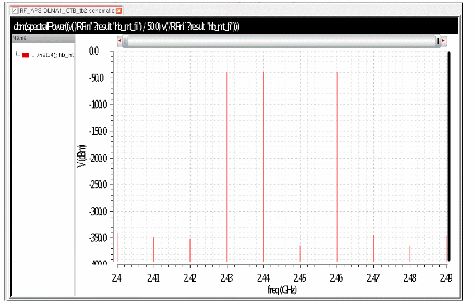
Below is a plot of the output when the variable prf is set to -40 (dBm).
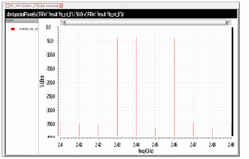
The amplitudes of the tones at 2.4G, 2.41G, 2.42G and so on are at the numerical noise floor of the simulation.
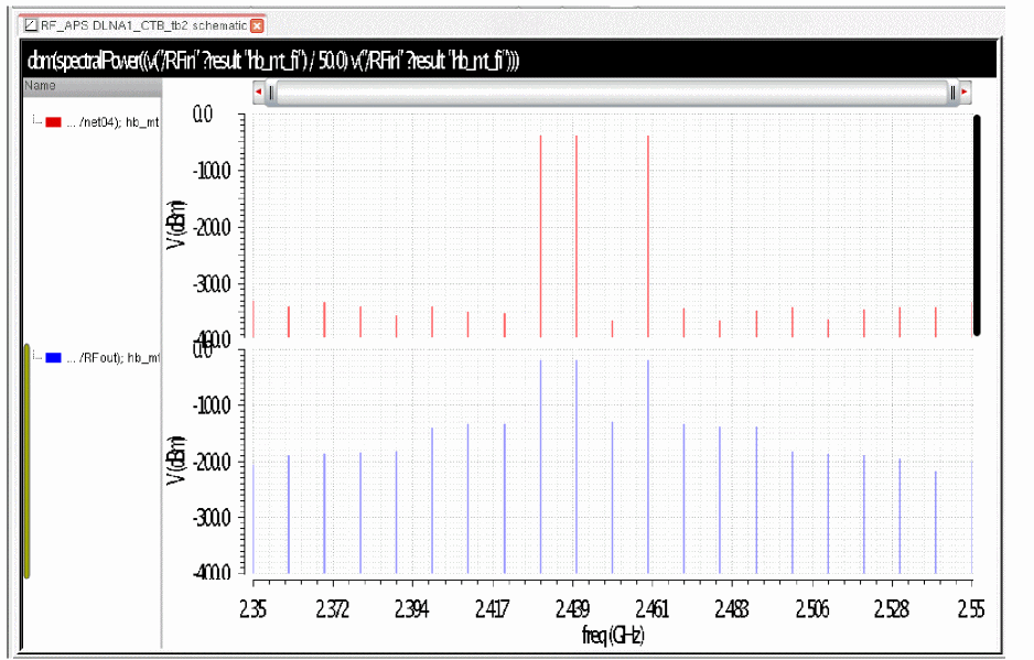
When these three frequencies are applied to a real system, the nonlinearity of the system produces mixing products. For example, 2.43G mixes with 2.44G to produce 10M. 2.44G mixes with 2.46G to produce 20M. 2.43G mixes with 2.46G to produce 30M. 2.43G, 2.44G, and 2.46G are first order terms, so 10M, 20M, and 30M are second order terms.
Now the 10M, 20M, and 30M terms can mix with 2.43G, 2.44G, and 2.46G. For example, 2.44G mixes with 10M to produce 2.45G. 2.44G is a first order term, and 10M is a second order term, so 2.45G is a third order term. 2.43G can mix with 20M to add an additional third order term at 2.45G. This leads to many harmonics that are actually produced, as shown below. The vertical axes have the same scale.
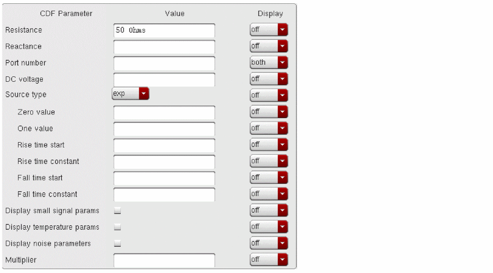
Exponential Waveform Parameters
To generate an exponential waveform from the port component, set the CDF parameter Source type=exp, as shown in the next figure.
Figure 9-11 Source type=exp in the Edit Object Properties form
The exponential waveform can generate one exponential pulse, and cannot generate a periodic signal. This it is not usable with SpectreRF.
When you specify the voltage on a port, you are specifying the voltage when the port is properly terminated, and not the voltage on the internal voltage source. Thus, the voltage on the internal source is set to twice the value specified on the port.
Zero value
The Zero value property is the time-zero value of the exponential waveform in volts.
One value
The One value property specifies the voltage that the signal transitions to at time equals zero plus. The default is one volt, which is unlikely to be what you want. Always set this property.
Rise time start
This property specifies the simulation time in seconds to begin the transition from the zero to the one value. The default is zero seconds.
Rise time constant
The Rise time constant specifies the time for the exponential waveform to reach 63 percent of the way from the zero value to the one value. The default is 0.075 percent of the stop time in the transient analysis.
Fall time start
The Fall time start specifies the simulation time to begin the transition from the one state to the zero state. The default is one percent of the transient analysis stop time.
Fall time constant
The Fall time constant specifies the simulation time for the exponential waveform to reach 63 percent of the way from the one value to the zero value. The default is one percent of the stop time in the transient analysis.
Bit Waveform Parameters
To generate bit sequence/string from the port component, select bit in the Source Type cyclic field. The bit source has four states: 1, 0, m, and z, which represent the high, low, middle voltage/current and high impedance state respectively. It allows patterns defining a sequence of bits. When the m state is specified, the output voltage is set halfway between the zero and one voltage.
Figure 9-12 Source type=bit in the Edit Object Properties form
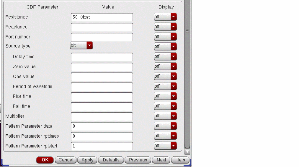
Delay Time
The Delay time property specifies the time the first bit in the string should be held before the first bit is generated.
Zero Value
The Zero value property sets the voltage when the pattern specifies a zero state. The pattern will be defined shortly.
If you intend to use the z state of the bit source, do not add a matching resistor across the port terminals, since this resistor will totally negate the high impedance state. Make sure that you halve the voltage values you want for the zero and one states when you use the port element to generate a bit pattern.
One Value
The One value property sets the voltage of the port when the pattern specifies a one.
Period of Waveform
The bit waveform type generates a bit stream where the period defines the period of one of the bits in the stream. For example, if the period property is set to 1n, then every nanosecond the bit switches to the next bit in the sequence.
Rise Time
The Rise time property specifies the transition time from the zero state to the one state.
Fall Time
The Fall time property specifies the transition time from the one state to the zero state.
Pattern Parameter data
This is the bit string, which is a series of the four states; 1, 0, m, and z. An example is 101100 (not separated by spaces) which would generate a 1, then a zero, then 2 ones in a row, and then two zeros in a row.
rptstart
This specifies the starting bit number when repeating. Default value is 1, which causes the first bit in the sequence to be the starting bit for the repeated pattern. The data repeats from the specified bit to the end of the bit string. The value of the parameter should be an integer from 1 to the length of the bit string.
rpttimes
This specifies the number of times the pattern should be repeated after the first sequence is generated. The default value is 0. which specifies that the pattern should not be repeated. When its value is negative, the string repeats forever. If a finite number of repeats is specified and the simulation time increases to a time after the last bit is generated, the output will maintain the state of the last bit in the sequence.
Bit Waveform Examples
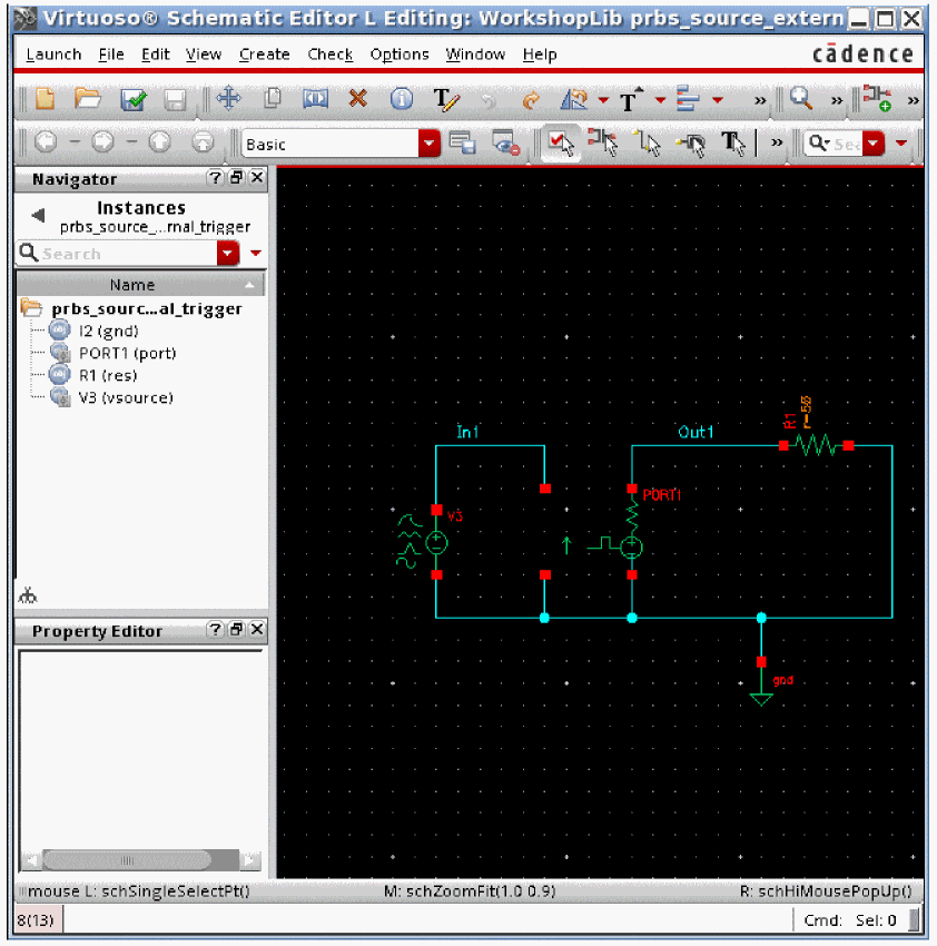
Here is the circuit that is used for all the examples.
The port with the sourcetype set to bit is on the left. Then there is a 1MOhm resistor, and a DC voltage source set to 900mV.
Example 1
Here is a property list for the first example.
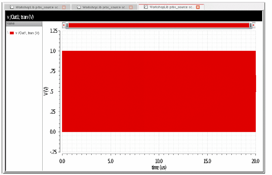
Here is the output signal which is Out1 in the schematic.
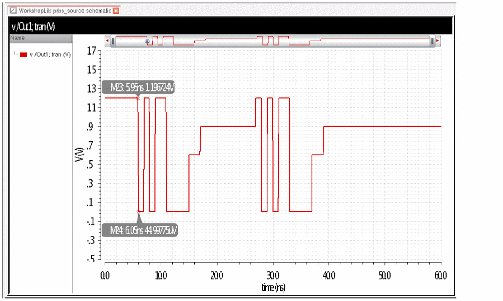
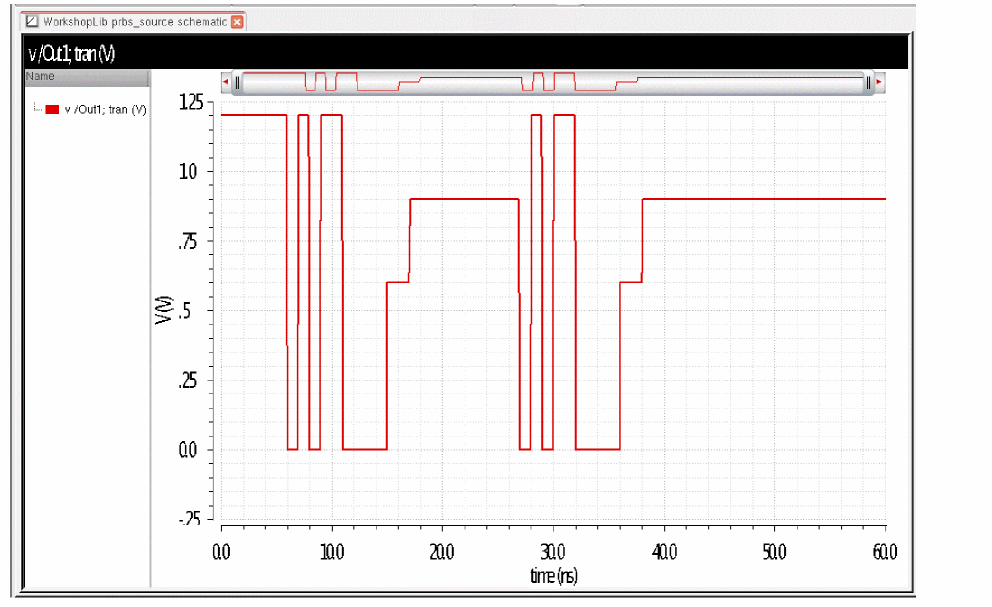
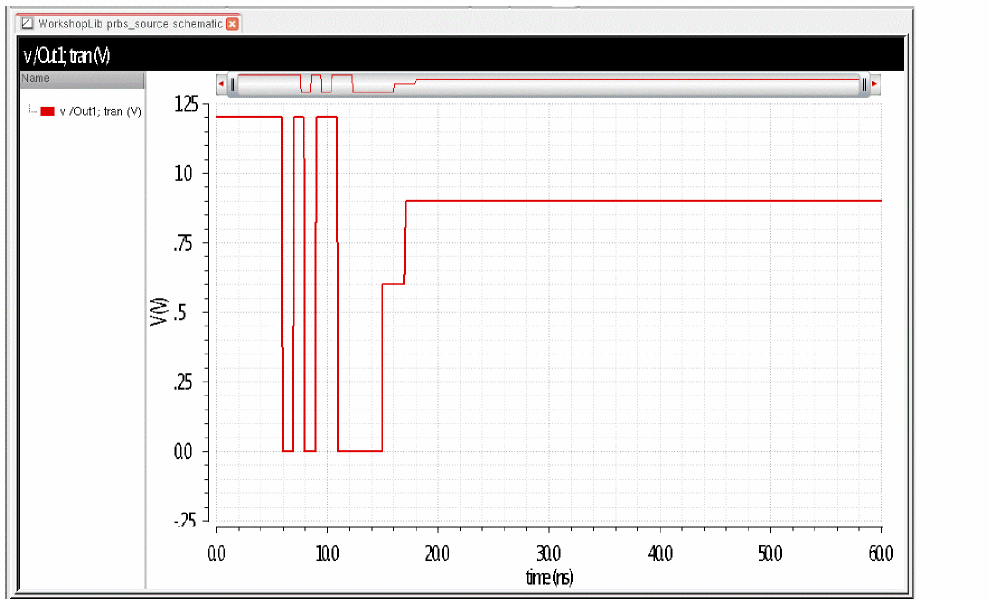
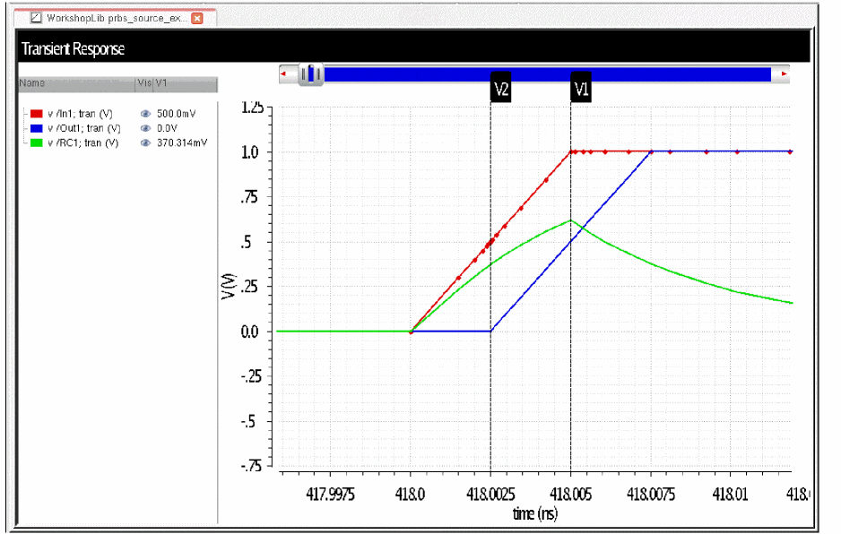
The delay time is 5n, and the bit period is 1n. This causes the signal to start at the first bit which is 1, and hold it for 5nsec. Then, it produces the first bit, which is 1 for the next nanosecond. If you look closely, you can see that the middle of the transition occurs at exactly 6nsec. The start of the transition is half the falltime before. The sequence is 1010110000mmzzzzzzzzzz. You can see the 0, 1, 0 transitions at 7nsec, 8nsec, and 9nsec. Then you see the two 1 states from 9nsec to 11 nsec, and the four 0 states from 11nsec to 15nsec. The next two states are middle states at 0.6v from 15nsec to 17 nsec. Then the output goes to high impedance, where the 900mv DC level at the output is seen. Rpttimes is set to 1, which repeats the pattern once, and the starting bit is the first bit in the sequence, which is a 1. At the end of the 900mv section, the signal transitions to the 1 state, and the entire pattern is repeated again. After the second pattern is done, the last state which is a z state is held after that.
Example 2
Here is the property list for the second example.
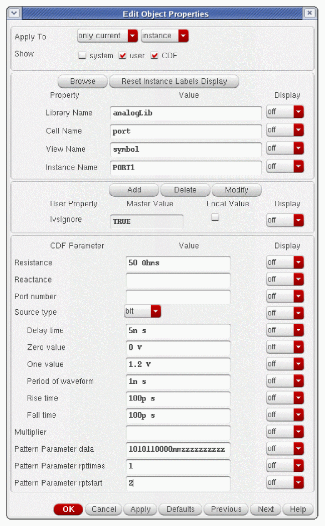
Everything is the same as the first example except for the repeat start, which is set to 2. This causes the second bit in the sequence, which is a 0, to be the starting bit. At the end of the first pattern, the signal repeats from the second bit in the sequence.
Example 3
Here is the property list for the third example.
PRBS Waveform Parameters
PRBS is an acronym for pseudo-random binary sequence. The PRBS source has three modes. It can be used to generate a maximum-length pseudo-random sequence. You can specify the beginning state and tap gains for a Fibonacci PRBS generator. A third mode allows reading an ascii file that describes the sequence of one and zero events to generate. To select this type of output, set the Source Type to PRBS.
For any mode, first you must define the output characteristics.
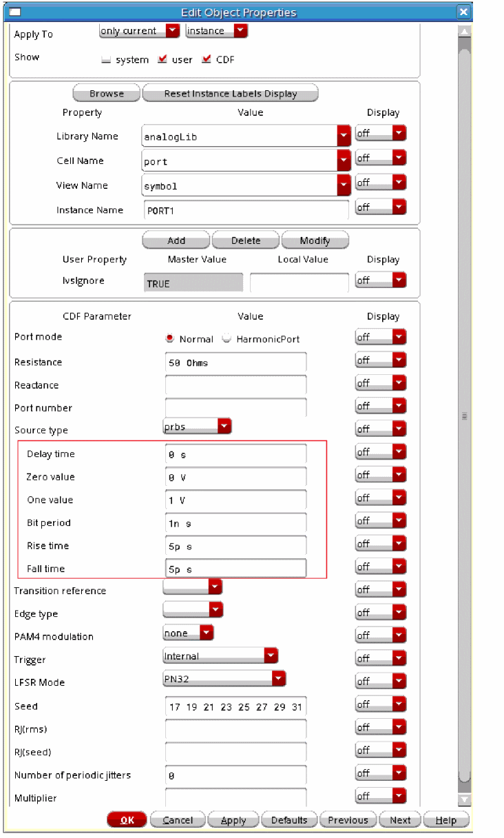
Delay Time
This specifies a time where the source stays at the zero value, and does nothing. The default is zero seconds. At the end of the delay time, the first bit will be produced.
Zero Value
This specifies the analog voltage to generate in the zero state. The default is zero volts. The port internally doubles the specified voltage as usual. To get the correct voltage when using the port, make sure that you add a matching resistor across the port terminals.
One Value
This specifies the analog voltage to generate in the one state. The default is one volt. The port internally doubles the specified voltage as usual. To get the correct voltage when using the port, make sure that you add a matching resistor across the port terminals.
Bit Period
This specifies the time of a single bit. It sets the trigger times between the zero and one state for the duration of a single bit. The transitions begin at the trigger event time. For example, if the Bit Period is 1n, then the first transition starts at 1nSec, the second transition starts at 2nSec, and so on.
Rise Time
This is the zero percent to 100 percent (by default) risetime for the transition from the zero state to the one state. The waveshape of the transition and the definition of risetime are settable.
Fall Time
This is the zero percent to 100 percent (by default) falltime for the transition from the one state to the zero state. The waveshape of the transition and the definition of risetime are settable.
Transition Reference
This specifies the thresholds for the rise time and fall time specification. This can be set to 0 to 100% (default), 10 to 90%, 20 to 80%, 30 to 70%, 40 to 60%, and Specify. When Specify is selected, the lower threshold must be entered. The upper threshold is calculated and is equidistant from the midpoint as the lower threshold. For example, if 22% is set for the lower threshold, 78% will be the upper threshold.
Edge Type
The waveform shape of the transition defaults to linear, which generates a traditional pulse with straight edges. Selecting halfsine causes sinusoidal rounding of the edges.
PAM4 modulation
The current PRBS source has binary output. When PAM4 modulation is set to PAM4, the prbs source generates four levels of binary instead of two, which allows two bits per symbol instead of one.
PAM4 mapping
This option is available only when you select PAM4 from the PAM4 modulation drop-down list. It specifies the mapping from a pair of bits to 4-level voltages. If you do not specify a value in this field, the default mapping is taken as 0132. This means:
Note that you are setting the bit period, not the symbol period. The symbol period is twice the bit period in PAM4.
The output shows four different voltages instead of two. The symbol period is 2ns.
LSFR Mode
This controls whether a maximal length sequence is generated, a file with a pattern of 1 and 0 states ia read and produced, or whether you specify the shift register, taps and starting the shift register state yourself.
Maximum Length Sequence LSFR Mode
The default is PN32, which generates a maximum length sequence (MLS) with a 32-bit shift register, and alternating 1 and zero states in the shift register as the starting state. To generate a different Maximum Length Sequence, change the seed parameter to define a different starting state, or define your own register, taps, and starting the state manually. Maximum length sequences using 2 to 32 bit shift registers are available. The table below defines the taps for each length of the available shift registers.
| Number of bits | Taps |
|---|---|
The taps are numbered from left to right, starting with zero and going through N where N is the number of bits in the shift register.
Below is an example with 0 to 100% risetime, linear edge type, with a 32 bit MLS set.
When this runs in the transient, first the alternating pattern of bits defined as the starting state of the shift register is produced, and then the sequence begins.
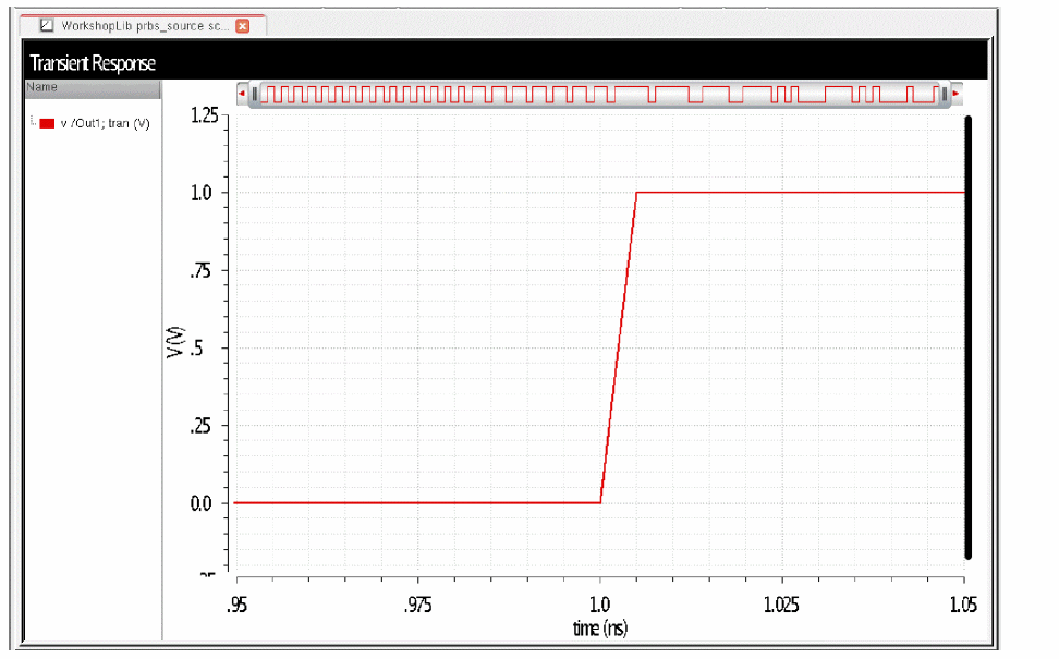
Looking closer, the transition begins at exactly 1nSec.
Specify Bit File LSFR Mode
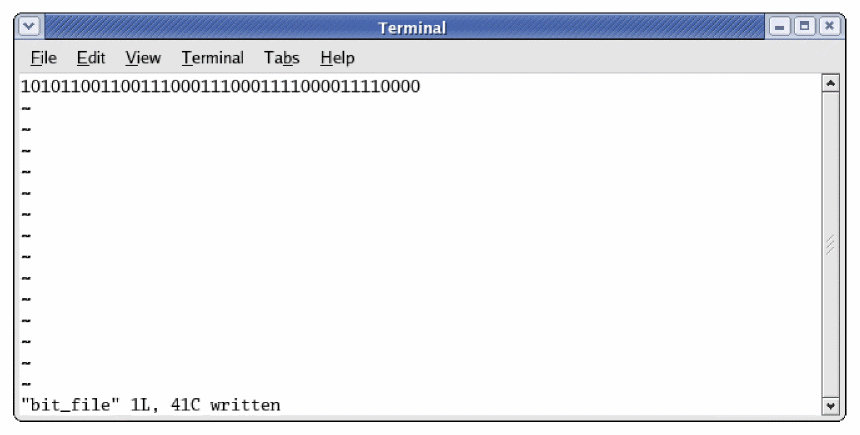
In this mode, an ASCII file with a sequence of 1 and 0 states is read. In this way, any arbitrary sequence can be used in the PRBS source. The states in the file are read from left to right, and if the time of the simulation exceeds the number of bit states in the file, the pattern will repeat. An example of a bit file is shown below.
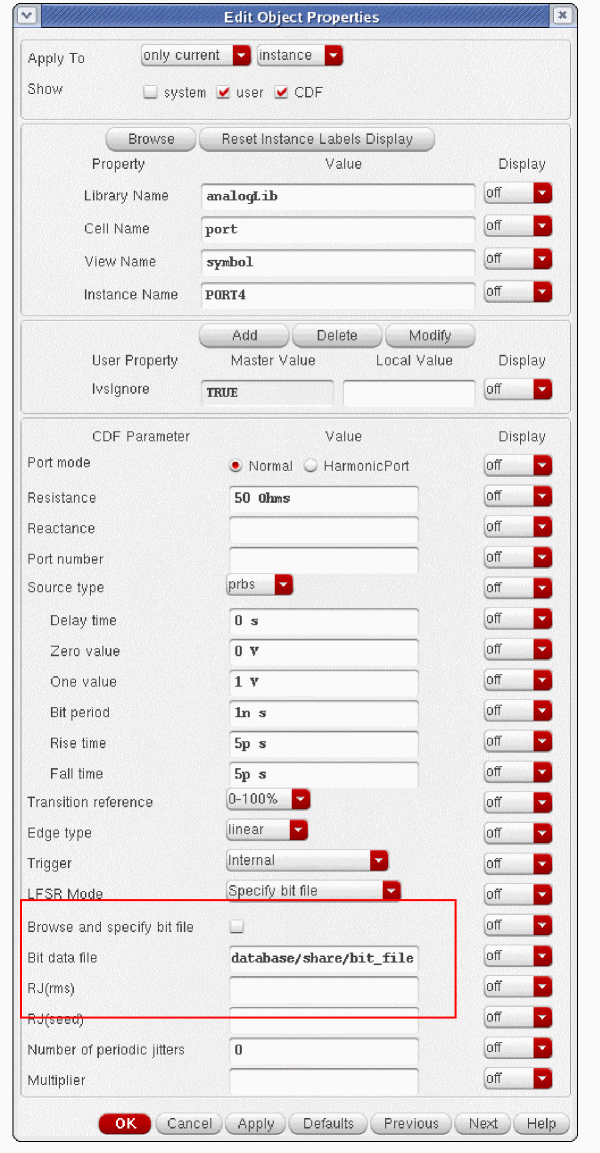
When the file with the bit pattern is available, set the LFSR mode to Specify bit file, and use the file browser to select the file. If you specify the filename manually, enter the complete path to the file for the file name. An example with the external bit file is shown below.
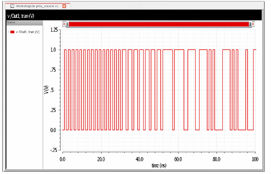
Note that the pattern in the file is reproduced, and repeats, as shown below.
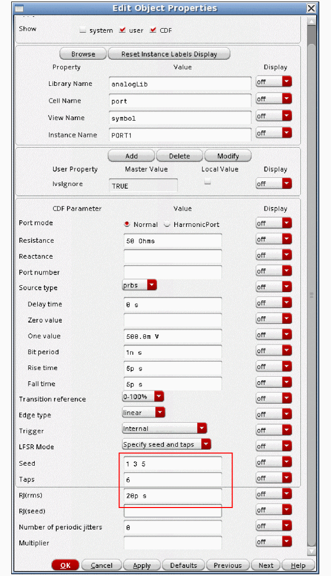
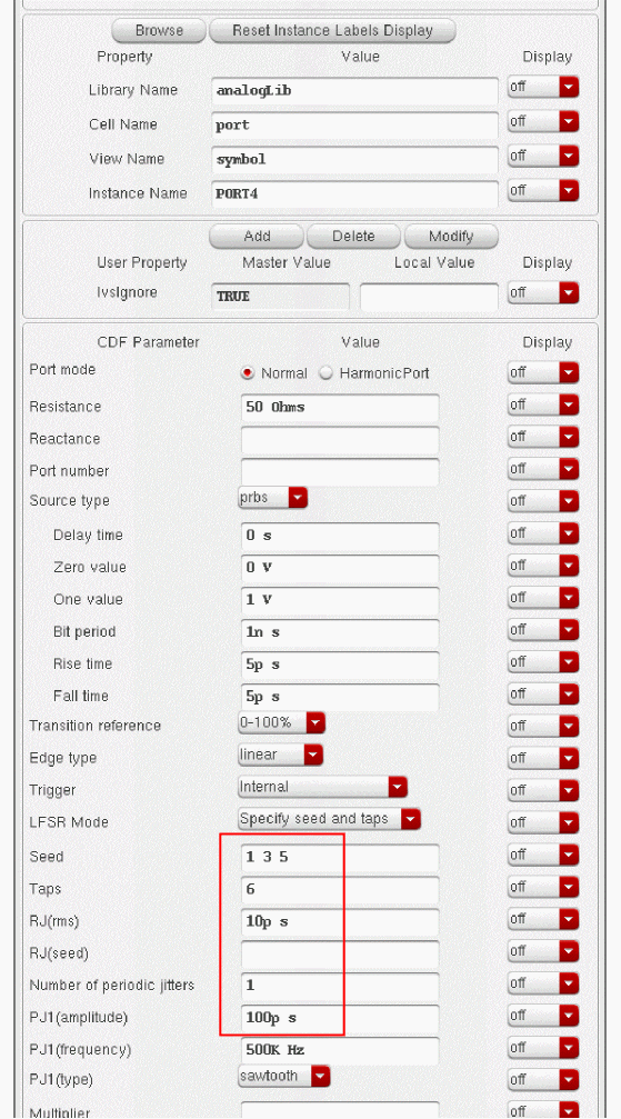
Specify Seed and Taps LFSFR Mode
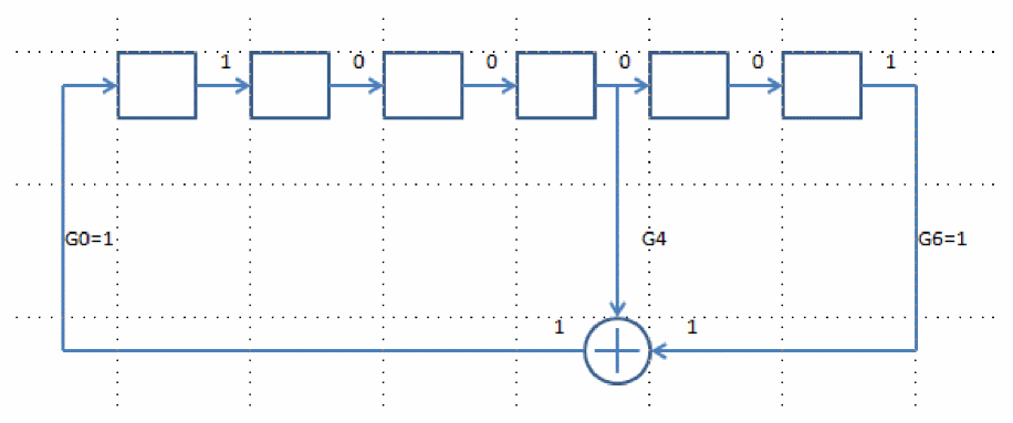
To use this feature, you must set the Seed and Tap information. The general configuration of a 6-bit Fibonacci shift register is as follows:
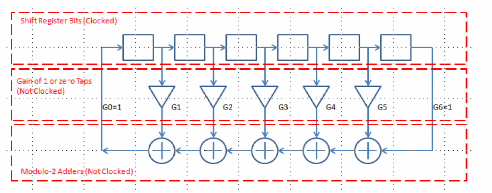
The boxes on the top are the shift register bits. The non-inverters in the middle can either be switched on or off, and are controlled by the taps vector. Taps zero and N (The taps at both ends of the shift register) are always on, which enables the circular connections. The shift register is clocked every period, and the bit shifts right. Depending on the setting of the feedback taps, different bits of the shift register can change the next bit that is loaded into the beginning (left) of the shift register. This logic is asynchronous. The adders at the bottom do modulo-2 addition, which is equivalent to an exclusive-or logic function.
Seed
This is a list of bit numbers to set to the one state that are used to preload the shift register at time zero. An example is 1 3 5, which would load the first, third, and fifth bits with the one state, and the rest of the bits to the zero state. If the size of the shift register is smaller than the data, the higher bit numbers are simply discarded. The default is to set all the odd bits to the one state.
Taps
This is a list of the taps to set to one, and also defines the length of the shift register. In the above example, the numbers 1, 2, 3, 4, and 5 can be specified. Additionally, 6 must be set to define the length to be 6 bits. The zero tap and the tap with the highest value in the Taps field are always set to 1. By convention, the first number is the number of bits in the shift register, and the next series of numbers are in descending order and control the gain of the taps. In Spectre, the numbers can be specified in any order, and the largest number sets the size of the shift register. For example, 6 4 2 (separated by spaces) specifies a 6-bit shift register with G2 and G4 set to one. The rest of the gains are set to zero, or an open connection. Also note that 6 4 and 4 6 give the same sequence. The largest number in the string sets the size of the shift register, and the rest of the numbers define which taps are on and off. If the Taps field has a single number, this defines the size of the shift register, and the values in the Seed field will endlessly circle through the shift register.
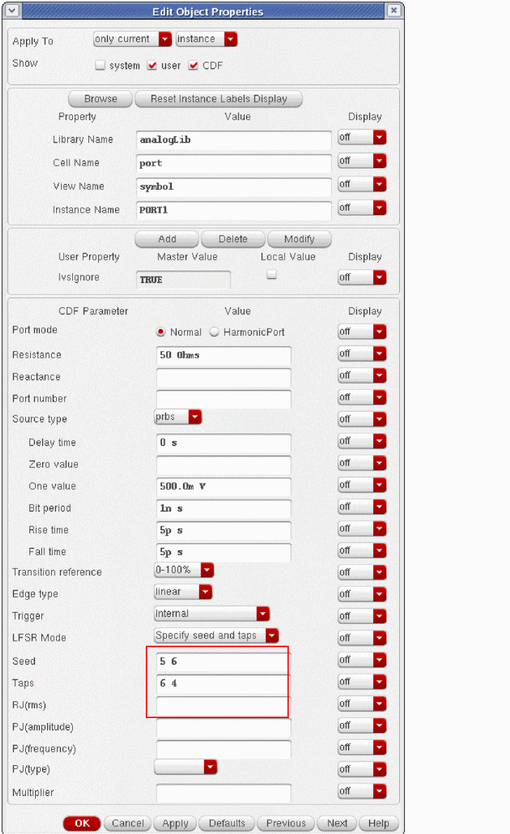
Detailed Example of Setting the Taps
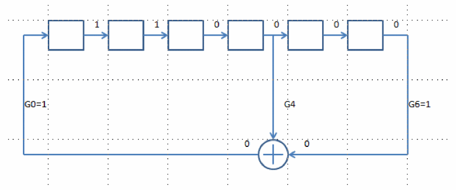
To manually specify the seed and taps, you must first set the LFSR Mode to Specify seed and taps. Next, set the size of the shift register, and define the taps. In this example, the size is set to six, and the fourth tap is enabled. The setting of the Taps property is 6 4 as shown below. To set the bits in the shift register to the digital pattern 000011, set 5 6 in the Seed property. This will load the one state into the rightmost 2 bits of the 6 bit shift register.
The internal bits get set, as shown below. When the tap is on, it is a connection. When it is off, it is an open. When the adders that are not shown have a zero on the top connection, they take the bit from the right, add zero, which just brings that bit to the left. The other adders just become wired connections.
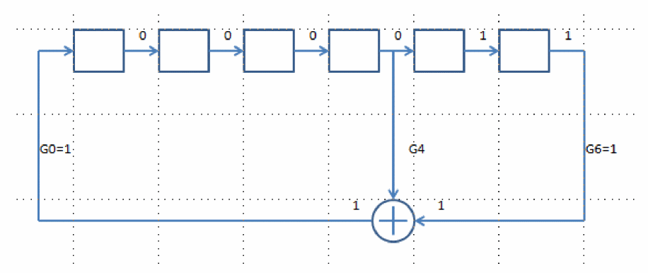
The taps vector enables G4, which brings the fourth bit from the left to the adder for that section. The adder sees a zero and a 1, so the output is 1. This 1 will be loaded in to the shift register at the next clock event.
At the next clock, the 1 from the output of the adder is loaded into the leftmost bit, and the contents shift right.
The output of the right bit is still 1, and the 4th bit from the left is still 0, so the output of the adder stays at 1.
At the next clock, the 1 is loaded in the leftmost bit, and the data shifts right.
Now, the adder sees zero on both inputs, so the output changes to zero. This is loaded in the next clock, and the data shifts right.
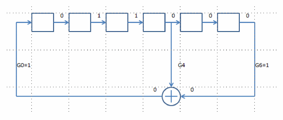
If you look at the sequence of the bits on the right side of the shift register so far, 1 1 0 0 has been generated. The sequence is from left to right. The first bit is a 1.
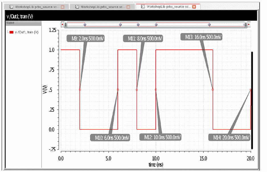
Continuing this exercise, it can be shown that the bits on the output should be 1 1 0 0 0 0 1 1 0 0 1 1 1 1 1 1 0 0 0 0 for the first 20 bits.
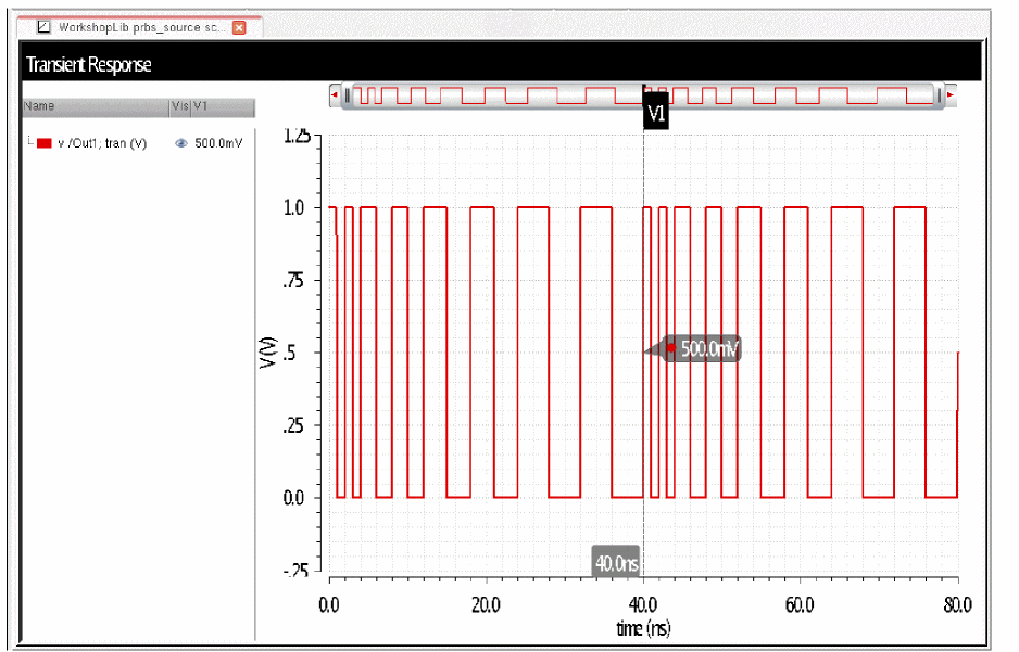
Now assume a bit period of 1nsec, The first bit, which is a 1, is generated from zero seconds to 1 nsec. The second bit, which is a 1, is generated from 1nsec to 2nsec. The third bit, which is a zero, is generated from 2nsec to 3nsec, The first transition from a 1 to a zero occurs at 2nsec. The bit sequence above would generate transitions at 2n, 6n, 8n, 10n, and 16n, which is shown in the result below.
Jitter Generation
The PRBS source can generate random jitter, periodic jitter, or a combination of both types of jitter. For periodic jitter, up to three periodic jitter sources can be specified. First, random jitter will be considered. The property for setting random jitter is RJ(rms).
This property defines one standard deviation for random jitter to be generated in the PRBS output waveform. Random jitter with a gaussian distribution will be generated on the transitions of the output waveform. This example has 20 psec jitter added, as shown below.
This is an optional property that can be used to generate different jitter sequences. Specify an integer in this field. The default value is 1.
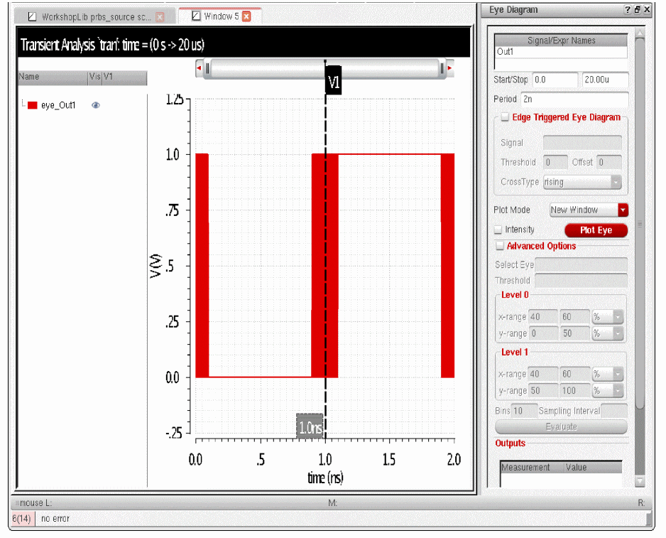
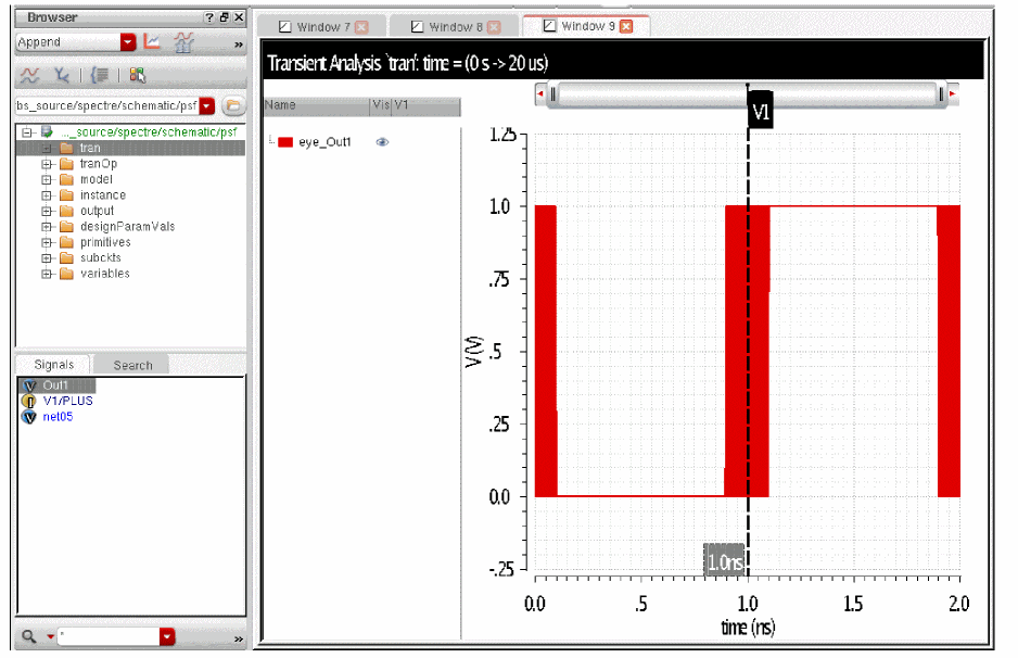
Next, this was run for 20 microseconds using the transient, and plotted in the waveform tool. To see the jitter, first select the trace, and then select Measurements - Eye Diagram.
The eye diagram assistant starts. The data has a periodicity of 1 nsec, To put all the transitions in the center of the eye, a 0.5 nsec Start Time is set, along with the 1 nsec periodicity of the output signal. The timing variations blur the transitions in the center.
To see where the wave is centered, a zoom operation was performed, and a vertical marker has been placed at 0.5 nsec.
In order to get standard deviation calculation, we need to modify the shift register so that it provides a periodic output. This is done in the example below by setting the seed to 13 5, which sets a 1 state in the first, third, and fifth bit, and then taps is set to 6, which rotates the pattern through the shift register endlessly. In this way, a square wave is generated with a periodicity of 2 nsec. This periodicity is needed in order for the standard deviation functions to work.
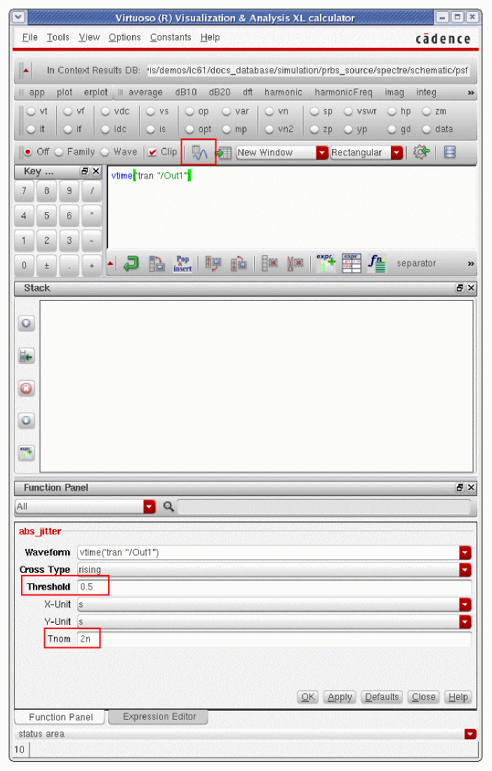
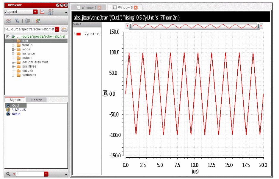
Now the transient is run for a large number of cycles. in the example below, it is run for 20usec, which gives 10,000 cycles of shift register output.
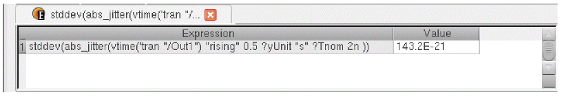
Select the trace, click the right mouse button and select Send To Calculator. This starts the calculator. Select the abs_jitter function. Set the threshold as appropriate for your circuit. 0.5 is appropriate for this example. Also set the period of the waveform in the Tnom field.
Now, plot the signal. The jitter plots, as shown below.
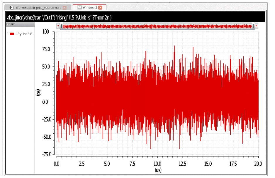
Now add the stddev function in the calculator. Send the result to a table.
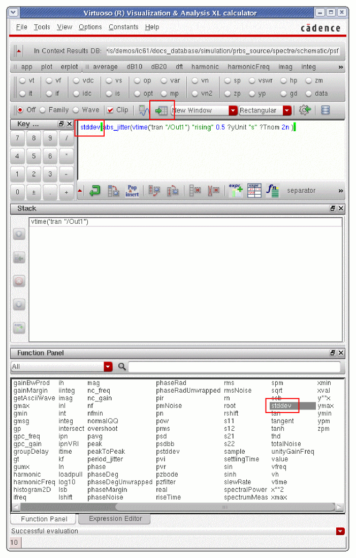
The result is very close to the 20psec setting in the prbs source.
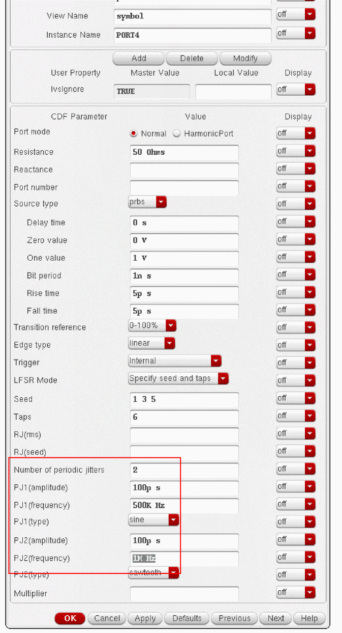
Periodic Jitter
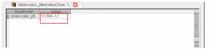
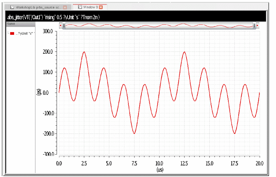
Periodic jitter can be generated in the prbs source by setting the number of periodic jitter sources, choosing the waveshape for each jitter source, setting the frequency of each periodic jitter source, and by defining the delta-T (peak) for each jitter source in the PJ(amplitude) field. Jitter waveforms can be sinusoidal, triangular, or square wave. Below is an example of a single periodic sinusoidal jitter source at 500KHz with 100psec peak jitter.
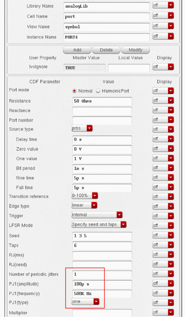
Run in the transient, and then send the waveform to the calculator. Apply the abs_jitter function as before. The jitter waveform is shown below.
The curve seems to indicate only the negative jitter. An eye diagram was plotted to check the actual timing of the edges.
Note that the jitter is actually centered at 1nsec, which is the timing of the noise-free waveform. The abs_jitter function takes the time of the first transition of the time-domain waveform as the center time of the jitter calculation. As a result, the center value can be skewed if the timing of the first edge is not noise free.
Below is an example of a triangle wave with 100psec peak jitter.
Again, with an eye diagram, the transitions are centered around 1nsec.
Two Periodic Jitter sources at the Same Time
Up to three periodic jitter sources can be set at the same time. Specify the number of periodic sources you want, and define the jitter parameters for each jitter source. An example with two jitter sources is shown below.
The resulting abs_jitter plot is shown below. Both jitter sources are in the output.
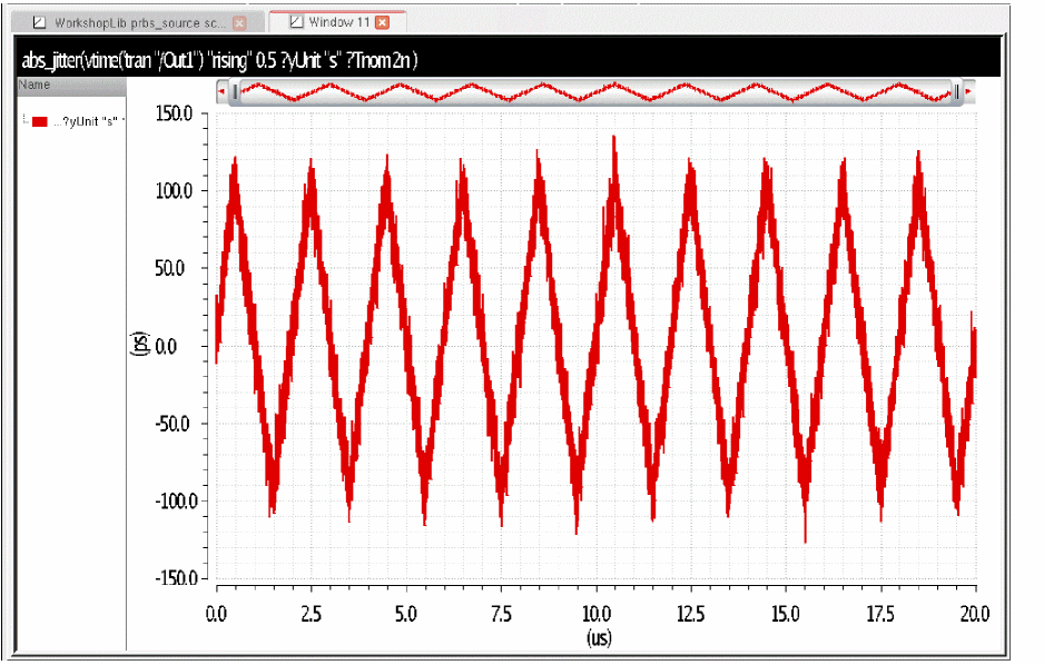
Random and Periodic Jitter at the Same Time
Both random and periodic jitter can be added at the same time. Below is an example of setting both in the prbs source.
The abs_jitter plot shows both random and periodic jitter
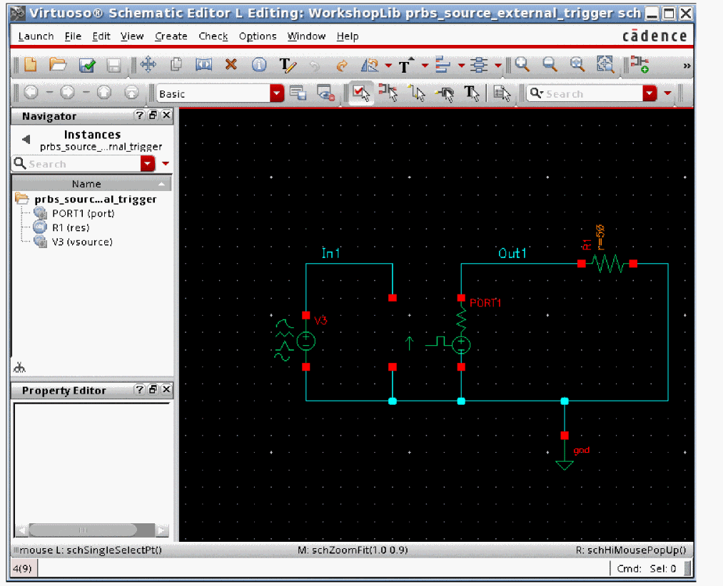
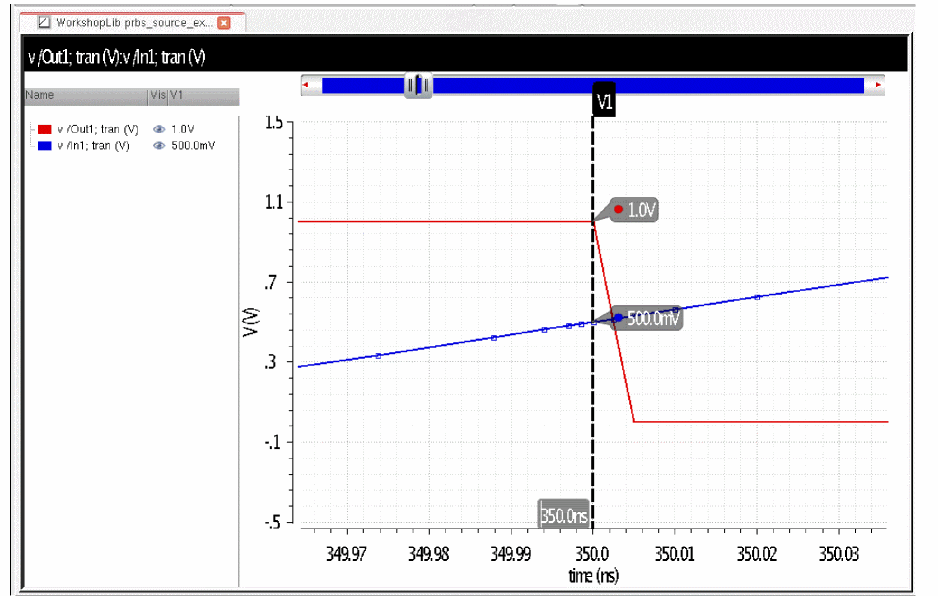
PRBS Mode External Triggering
When the prbs source is externally triggered, the schematic Pcell redraws for the source, and two control terminals are added to the left of the source. This is shown below.
When the source is externally triggered, periodic and random noise generators are turned off. The properties form specifies the voltage level for the trigger and the edge mode for the trigger. In the example below, the trigger threshold is 0.5 Volts and the trigger is on the rising edge.
Note that the jitter terms are greyed out, indicating that the jitter is not available in the external trigger mode.
When the threshold is reached on the input waveform, the output begins the transition to the opposite state. The timestep is actively controlled in the region of the trigger threshold to make the signal trigger very accurately. In the waveform window below, the blue trace is the input, and the trace symbols are on and mark the timesteps actually used in the simulation. As the threshold is reached, the timestep is actively managed so that the crossing is accurately detected.
The jitter is also very small, as seen below.
The calculator expression is shown on the left, and this is the same expression used before in this section to calculate the jitter.
PRBS Source with External Triggering Using a Pulse or PWL Signal
The external triggering capability of the prbs source depends on being able to calculate the slope of the input signal in order to accurately trigger at the specified voltage. The pulse and pwl sources guarantee timepoints at the corners of the waveforms, but they do not guarantee timepoints during the transition, especially if the transition is short. In that case, the prbs will trigger on the timepoint on the end of the transition as shown below.
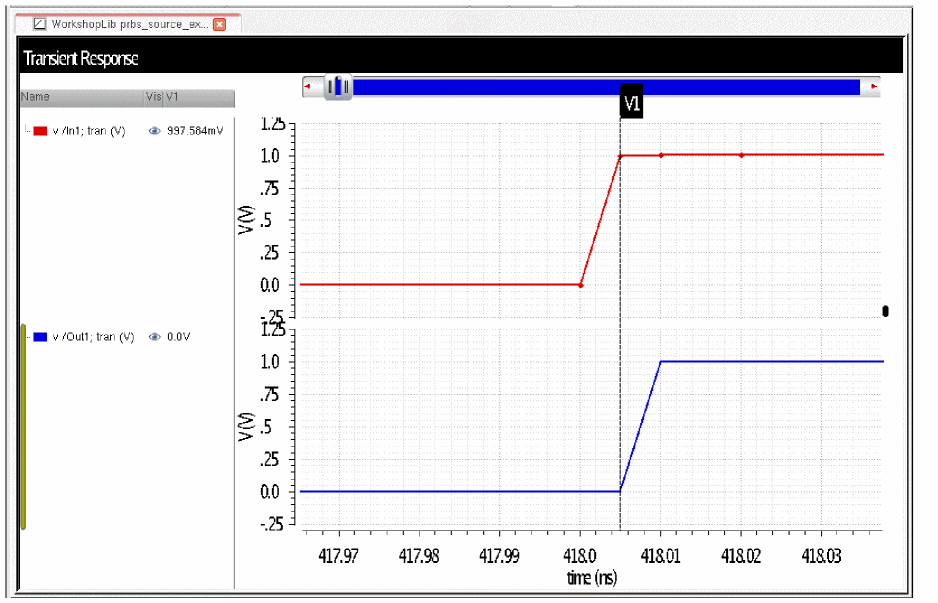
The threshold for the trigger is 0.5 volts, and the input signal is the red trace. The actual timepoints of the input (red trace) are turned on, and the output starts its transition when the input is at 1 volt instead of at 0.5 Volts. This adds a slight delay in the prbs output, which in many cases is not significant. If you need to trigger on the actual threshold, then add a resistor and capacitor across the source as shown below. Set the R*C product to be the risetime of the input signal.
Adding these components adds numerical integration, and the error of this integration is controlled by Spectre by adding appropriate timepoints. This establishes a slope of the input signal so the trigger event can happen at the desired threshold of 0.5 volts in this example as shown below. The green trace below is the junction of the resistor and capacitor that was added to the circuit. Again, the timepoints are turned on for the input trace.
Keep the R*C product equal to the risetime of the pulse source or slightly less so the timestep is not excessively reduced for a long period of time.
Oscillator Macro Parameters
The oscmacro source can be used to generate oscillator waveform and noise in pss-pnoise and hb-hbnoise analysis. The oscmacro source does not generate noise in transient analysis.
File Name
Specifies the file name containing the harmonics and noise data results from hb and hbnoise analyses. For more information, see Creating an Oscillator Macro Source.
Freq scale
Specifies the frequency scaling factor. This is a multiplier for the frequency of the source. The default value is 1.0 which uses the frequency in the specified file.
Amplitude scale
Specifies the amplitude scaling factor. This is a multiplier for the amplitude of the output. The default value is 1.0 which uses the amplitude in the specified file.
Noise Parameters
The noise parameters include Noise temperature, Noise Entry Method, Noise file name, Noise type, Interpolation method, and Noise/Frequency points.
The Noise type selection sets one of two basic modes. When Noise type is set to Noise Voltage, pure noise voltage is injected for the noise analysis. In this mode, you specify frequency-volts-squared per Hertz pairs either in a file, or manually entered into the form. The second mode is to inject pure phase noise. In this mode, you specify frequency—ssb phase noise in dBc/Hz pairs. Phase noise is only available when the Source type property is set to sine and pulse.
Voltage noise is observed in transient noise, but phase noise is not.
The first example shown below has voltage noise injected. The default linear interpolation should be used when the noise data has linear spacing. If the noise data has log spacing, log-log interpolation will cause the noise analysis to be more accurate.
When phase noise is selected, log-log interpolation is always used. The frequency terms for the phase noise data should be the offset frequency from the carrier. The noise term should be single-sideband phase noise (ssbphasenoise) in dBc/Hz. The phase noise will be injected above and below the frequency for the first sinusoid the source produces.
An example of phase noise is shown below
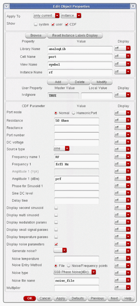
Noise temperature
Noise Entry Method
You can select one of the two ways to enter noise data, either by specifying a File name or entering a series of Noise/Frequency points.
Noise file name
If Noise Entry Method = File is selected, you enter the name of the file containing the noise data in the form of frequency-noise pairs. In your file, list the
Figure 9-13 Display noise parameters: Noise Entry Method=File
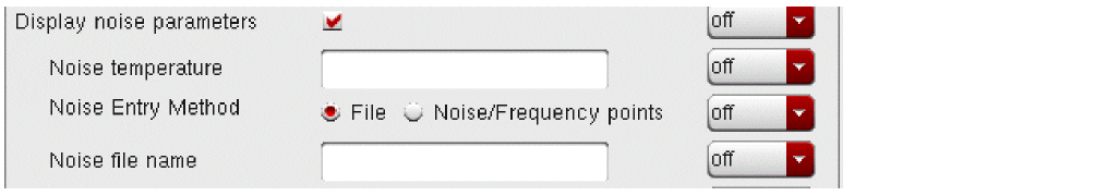
Num. of noise/freq pairs
If the Noise Entry Method is set to Noise/Frequency points, you specify the Number of noise/freq pairs
The example below has the Number of noise/freq pairs set to 3.
Figure 9-14 Display noise parameters: Noise Entry Method=Noise/Frequency Points
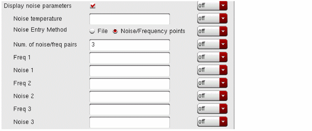
Small-Signal Parameters
Display small signal params
If selected, the Edit Object Properties/Add Instance form expands to show the small-signal properties PAC Magnitude, PAC Magnitude (dBm), PAC phase, AC Magnitude, AC phase, and XF Magnitude.
Figure 9-15 Display small signal params
When you specify the voltage on a port, you are specifying the voltage when the port is properly terminated, and not the voltage on the internal voltage source. Thus, the voltage on the internal source is set to twice the value specified on the port. The same is true for the values for the transient, AC, and PAC signals. However, the amplitude of the sine wave in the PAC and transient analysis can alternatively be specified as the power in dBm delivered by the port when terminated with the reference resistance. The PAC magnitude property is used by pac, hbac, and qpac. The XF Magnitude property is used by xf, pxf, hbxf, and qpxf.
PAC Magnitude
The peak periodic AC analysis magnitude. Setting this value to unity is a convenient way of computing the transfer function from this source to the output.
You can select either PAC magnitude or PAC magnitude (dBm), but not both. If PAC magnitude has a value, the PAC magnitude (dBm) field is grayed out. The PAC magnitude property is used by pac, hbac, and qpac.
PAC Magnitude (dBm)
The periodic AC analysis magnitude in dBm (alternative to PAC magnitude). You can select either PAC magnitude or PAC magnitude (dBm), but not both. If PAC magnitude (dBm) has a value, the PAC magnitude field is grayed out. The PAC magnitude(dBm) property is used by pac, hbac, and qpac.
PAC phase
The periodic AC analysis phase. The value must be a real number. The default value is 0 and the units is in degrees.
Typically, only one source in the circuit has a PAC magnitude set to a value other than zero, and many times it has a PAC magnitude=1 and PAC phase=0. However, there are situations where more than one source has a nonzero PAC magnitude. For example, applying a differential small-signal input could be done with two sources with the PAC magnitudes set to 0.5 and the PAC phases set to 0 and 180. The PAC Phase property is used by pac, hbac, and qpac.
You do not specify the PAC frequency in the port Edit Object Properties form. Instead, you set the PAC frequency in the PAC Choosing Analyses form. For example, when making an IP3 measurement, you set the PAC frequency to a variable value in the Choosing Analyses form. Then, you enter the same variable in the PAC Amplitude (or PAC Amplitude dBm) field of the port Edit Object Properties form.
AC Magnitude
The peak small-signal voltage for the ac analysis in volts.
AC phase
The ac small-signal phase in degrees.
Typically, only one source in the circuit has AC Magnitude set to a value other than zero, and many times it has an AC magnitude=1 and AC phase=0. However, there are situations where more than one source has a non-zero AC magnitude. For example, you can apply a differential small-signal input with two sources with the AC magnitudes set to 0.5 and the AC phases set to 0 and 180.
XF Magnitude
This property is seldom used. It specifies the transfer function analysis magnitude. This is used by xf, pxf, hbxf, and qpxf.
Temperature Effect Parameters
Temperature effect parameters include Linear temp. coefficient, Quadratic temp. coefficient, and Nominal temperature.
Display temperature params
If the check box is selected, the Edit Object Properties/Add Instance form expands and the following three parameters appear in the form: Linear temp. coefficient, Quadratic temp. coeff., and Nominal temperature.
Figure 9-16 Display temperature params
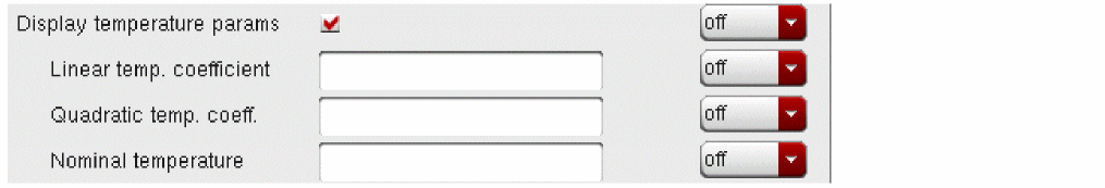
Linear temp. coefficient
This property sets the first order (linear) temperature coefficient of all the voltages specified for any waveform in the port. 0.01 entered in the Linear temp. coefficient field is interpreted as a one percent change per degree Celsius. If the number is positive, the voltages increase with temperature. If the number is negative, the voltages decrease with temperature. If the temperature moves far enough, the values can become negative.
Quadratic temp. coeff.
This property sets the second order (quadratic) temperature coefficient of all the voltages the source generates. 0.01 causes a change in value of one percent per degree squared.
Nominal temperature
Simulating Tabulated S-Parameters Using the Nport Component
Nport from analogLib provides a generic way to incorporate an S-Parameter file into a circuit simulation. The nport component allows you to set the number of ports, and when this is done, the schematic symbol re-draws with the number of ports shown. There is also n1port, n2port, n3port, and n4port in analogLib, which have a fixed number of ports. These components are provided for legacy purposes only, and should not be used in current simulations.
For the frequency-domain based analyses, such as ac, noise, xf, stb, pz, harmonic balance, hbac, hbxf, and hbnoise, the S-Parameter file is used directly in the frequency domain. For the DC and transient based simulations dc, tran, and shooting, a time-domain model must be created from the frequency-domain description in the S-Parameter file. This is a non-trivial process.
In general, there are two different ways to create a time-domain model from an S-Parameter file. One way is to do a rational fit, which attempts to match the frequency domain description using a combination of poles, zeros, and gain blocks. The other way uses a convolution-based approach. This approach calculates the impulse response, and then creates a time-domain model based on the impulse response.
Regardless of the method, there are fundamental requirements for the S-Parameter file. These are:
-
The file must contain a frequency point that is low enough so that when the DC point is extrapolated, the DC point correctly defines your circuit behavior.
This is a fundamental requirement. To run a transient, first you need to run the DC analysis to capture the time-zero timepoint. If the first frequency in the file is not zero frequency, then a zero-frequency point must be extrapolated. If the first frequency in the S-Parameter file is not low enough to accurately represent the real DC characteristics of the system, the DC extrapolation will be incorrect. - The phase of the DC point must be zero or 180 degrees.
-
The frequency-domain data must be dense enough to accurately describe the transfer function.
Smooth transfer functions without local complex behavior might need relatively few datapoints. Systems with complicated behavior need to have enough datapoints to capture the behavior well enough so that when the data is interpolated between the given points, and the interpolation error is small.
For bandpass filters, make sure that data from near zero Hz through at least the frequency of the highest harmonic in the simulation is present in the S-Parameter file. -
The frequency data must exist to a high enough frequency so that harmonics of the system are accurately simulated.
If your S-Parameter file has data only through the second harmonic of the input signal and you are calculating six harmonics in a large-signal analysis, just note that the S-Parameter data above the second harmonic is extrapolated. The simulation is not based on real data, and as a result, it is different from the real system. If you want your simulation to be accurate for the harmonics you are simulating, make sure that the S-Parameters themselves go high enough in frequency. - As a strong suggestion, regardless of the source of the data, plot the data from your S-Parameter file before you simulate. The plot for all the S-Parameters should plot in a clockwise arc with no sudden jumps. These discontinuities cause large inaccuracies in the transient model. Spectre now checks for discontinuities in the S-Parameter data.
To plot an S-Parameter file directly in the waveform tool, the file format must be in Touchstone1 format. Here are the steps required to plot an S-Parameter form an S-Parameter file.
- From the ADE Explorer window, select Tools-Waveform.
-
In the waveform tool, select File-Open Results, and browse to the location of the S-Parameter file.
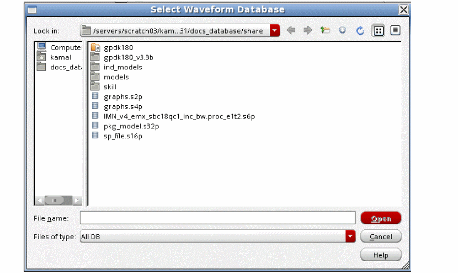
-
When the file is selected, the waveform tool has the path to the results at the top-left and the S-Parameter filename at the bottom. If you started from ADE Explorer, you may also have the path to the psf file on the upper left.
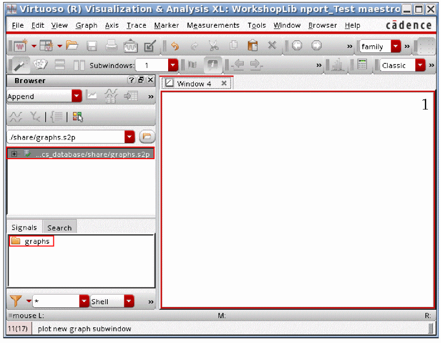
-
Double-click the filename. The S-Parameters in the file are displayed.
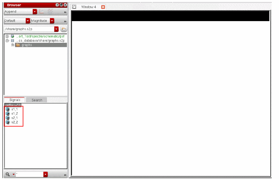
-
On the upper left, select Impedance or Admittance. This tells the waveform tool to plot on a Smith Chart.
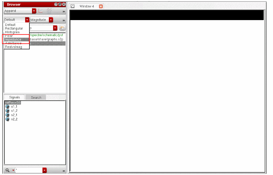
-
Click one of the S-Parameters. Click the right mouse button and select Move to Plot Signal. The signal plots.
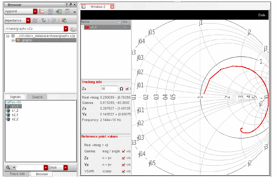
Potential Problems with S-Parameter Files
Not all frequency domain descriptions are causal. This is a fundamental requirement for the time-domain model to be accurate. When Spectre reads in an S-Parameter description and causality is being checked, the transfer function from the highest frequency in the S-Parameter file through three times the highest frequency in the S-Parameter file is adjusted to enforce causality. Frequencies above three times the frequency in the S-Parameter file should be avoided.
Convolution-Based Method
The convolution-based method is strongly suggested for most simulations. This method is used when the interpolation method is set to linear or spline. The default interpolation method is linear, and the convolution-based method is the default.
The convolution-based method samples the frequency-domain data, and then calculates the impulse response for that frequency description. Then a Fourier transform is used to create the DC and time-domain model.
Considerable development has been made in MMSIM12.1 so that the only thing that should be required is to set the S-parameter file name, the interpolation method, and the number of ports. The default settings are strongly recommended for all other parameters. By default, the impulse responses are cached. This allows the reuse of previously computed impulse response files, thereby saving a lot of time in simulations after the first time the simulation is run. If multiple instances in the schematic use the same S-Parameter file, the impulse response is calculated only once. The impulse response may need to be recalculated if you specifically set some of the properties that are available in the nport. Except for the Passivity parameter and the Accuracy parameter, changing any other property is highly discouraged unless you are an expert in simulating S-Parameters. The old Impulse response will not be erased. If you switch back to the previous settings in the nport, those files will still be available, and will still be reused. The location of the files depends on the setting of the nportfiledir option which is documented later.
S-Parameter files with a large number of ports require lengthy calculations. In many cases, although there are a large number of ports in the S-Parameter file, only a small number of ports are actually connected in the circuit. This is common for package models. Starting with the MMSIM 12.1.1 release, the number of calculations can be reduced by eliminating the unused ports from the circuit, thus, improving the simulation time. This is done at the beginning of the simulation, and affects all the analyses that are specified to be run. If there is a component in the circuit connected to a port in the circuit, it is kept. If there is no connection, this port is removed. If you desire to monitor the output of a port that is not connected, add a large resistor to ground on this port so you can see what appears on this connection point. By default, if there are 20 ports or more, and 80% or less are actually connected to other components, the nport will be compressed. There are also global options in the Simulation - Options - Analog form (Components tab) to set compression explicitly.
Rational Fit Methods
There are two rational fit methods. In general, these methods fit the data using poles and zeros to match the S-Parameter data. Of the two methods, bbspice is preferred. Bbspice is used to do the rational fit. The product bbspice has many desirable features such as non-causal data identification that are not implemented in the nport. For this method, set the Interpolation method to bbspice.
Using the nport Component
The nport symbol is a schematic Pcell, which redraws when you change the number of ports. The symbol has two different modes. At the top of the properties list, is a selection called Common reference, which is a check box. If the item is not checked, plus and minus pins will be displayed for all the individual ports. If the check box is selected, then the symbol redraws with a single common ground reference pin at the bottom of the symbol. This eliminates the need to add ground connections to each port of the symbol. The check box is highlighted in the properties list below.
Figure 9-17 nport Component Edit Object Properties Form
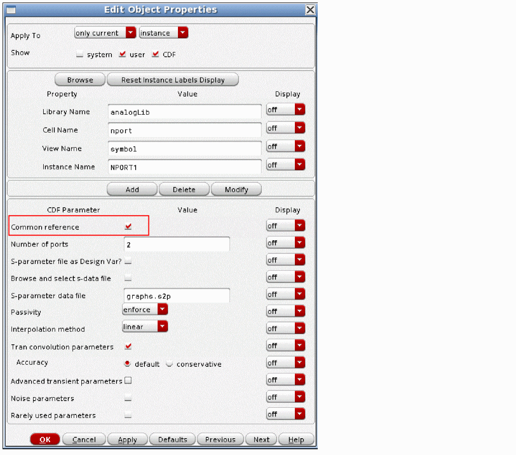
The symbol without the selection is shown on the left in the figure below, and the symbol with the selection is shown on the right.
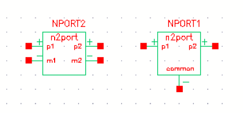
Use the
Figure 9-18 nport Component Edit Object Properties Form
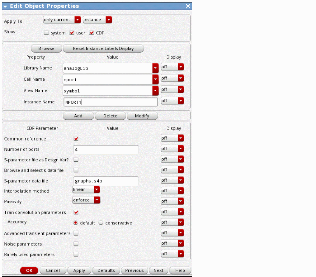
- Select the nport component from analogLib.
- Place the nport component in the schematic window.
- Set whether you want a single ground terminal on the nport symbol or not.
- Set the number of ports that are in the S-Parameter file.
-
In the Schematic window, highlight the new component and then choose Edit – Properties – Objects, or use the bindkey you have set up for setting properties.
The Edit Object Properties form for the nport component is displayed. -
Click the file browser button located to the right of Browse and select the s-data file in the properties form. From the browser, select the S-Parameter file.
Alternatively, type in the S-Parameter data filename. If you specify just the filename in the port component (not the complete filename starting from slash), then in ADE Explorer, select Setup - Simulation Files, and enter the path to the directory that contains the S-Parameter file in the Include Paths section. This is necessary so that the file can be found.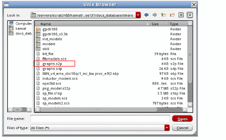
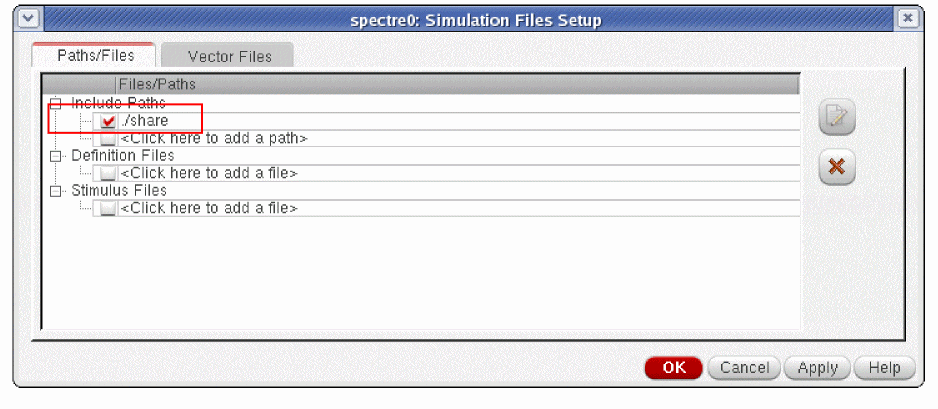 You can also specify an S-parameter file as a design variable. To do this, select the S-parameter file as Design Var? check box and enter the name of the variable in the S-parameter data file field. However, this action does not add the file in ADE Explorer automatically even when you select the Variables - Copy from CellView menu option. You need to manually add a design variable in ADE Explorer and enter the file name
"/<path>/<file_name>.s2p"surrounded by quotes in the Value field. - Although the properties form is labeled S-Parameter data file, it can also be a Y-Parameter or Z-Parameter file. Spectre recognizes all three formats. It is labeled this way because S-Parameter files are more common than Y or Z-Parameter files.
-
Set the Interpolation method cyclic field.
The linear and spline values are usually preferable to rational. If you want a rational fit, bbspice is preferred over rational. In general, the recommended method is linear.
Linear and spline control the sampling of the S-Parameter data for the convolution-based method. In both methods, the S-parameter data is sampled using a linear frequency spacing from zero to three times the highest frequency in the S-Parameter data file in order to calculate the impulse response of the transfer function.Note that when the S-Parameter file is for a physically large structure like a package model, because of the physical size of the structure, the inductance drops starting in the range of 100KHz to 1MHz. To correctly model this behavior, you require data in the S-parameter file that accurately describes this behavior, and it requires a huge number of frequency sample points in order to get a correct time-domain model.
When linear is selected as the interpolation method, linear interpolation is used to get a datapoint needed in the sample that is not directly in the S-Parameter file. Spline uses a cubic spline algorithm. Cubic spline can occasionally introduce errors when there are rapid changes in the transfer functions defined in the S-Parameter file near the sample point.
When the data in the S-Parameter file is dense, linear and spline produce comparable results. When the data in the S-Parameter file is sparse, non-physical results can be introduced because of the wiggles that can be introduced by a polynomial fit. Linear is usually a better choice when the data is sparse.
When you select rational, four new fields are displayed. For information about these fields, see Controlling Rational Fit Accuracy. -
Specify whether you want the passivity check to run. Setting Passivity to no causes no passivity check to be run. Setting Passivity to check, which is the default, will run a passivity check, and the result of the check will be sent to the Spectre output window. The S-Parameter file will be used as specified.
If Passivity is set to enforce, the passivity check will be run, and the S-Parameter file will be changed as necessary to ensure the passivity of the result. Note that this will change the S-Parameters as specified in the file if a non-passive entry is detected. The no, check, and enforce options are applicable only when the interpolation method is set to linear, spline, or rational.
If Interpolation Method is set to bbspice, passivity may be set to fit_weak_enforce or fit_enforce. The default value is fit_enforce and with this setting the simulator always attempts to create a passive simulation model and favors passivity over accuracy. When Passivity is set to fit_weak_enforce, the simulator does not create a passive model if the passivity enforcement phase results in a significant accuracy loss. -
If exceptional accuracy is desired, select Conservative for the Accuracy default. This will cause more frequency-domain sample points, and produce a more accurate impulse response at the cost of runtime. Default accuracy is set tight enough that Conservative should only be needed in rare instances.
When the DC or transient-based simulation is run, Spectre provides information about the S-Parameter file and the impulse response file in the output window.
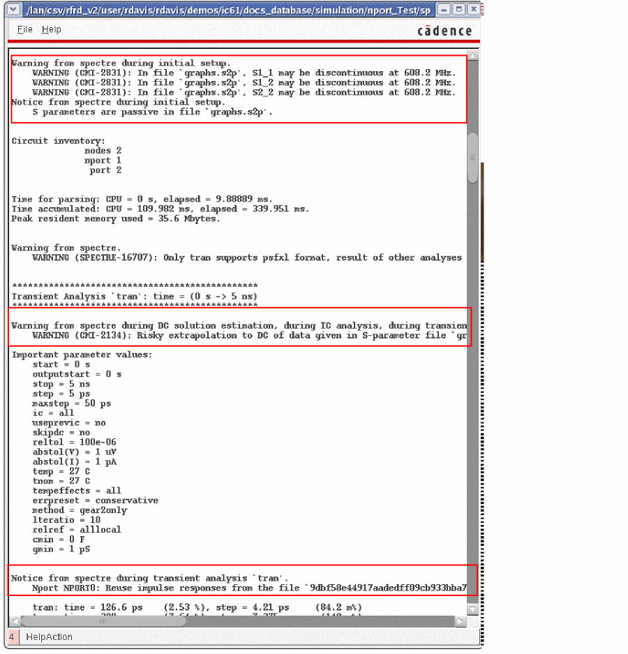
Global Options for Fitting Parameters
The global options for the passivity check can be set in the Simulator Options form by selecting Simulation - Options - Analog, and then selecting the Component tab.
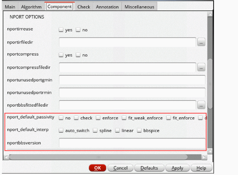
nport_default_passivity
This is the global option for checking and enforcing passivity of S-parameter for all nport instances.
nport_default_interp
This option sets the default interpolation method.
nportbbversion
This option sets the bbspice version to be used for S-parameters modeling. Possible integer values are: 1 (deprecated; used in SPECTRE 19.1 and earlier versions) and 2 (default in SPECTRE 20.1).
Nport Compression
In cases where package models are used, many ports may be specified in the S-Parameter file, but only a small number of ports are actually connected to the circuit for simulation. Although the nport caches the data from the S-Parameter file, with a large number of ports, the extraction time can be an issue. To speed these extractions, the S-Parameter file can be compressed, which removes the unused ports from the extraction and from the simulation result, but causes the extraction to be considerably faster. The extraction time is reduced to the square of the connected port fraction. If 10% of the ports are connected, the extraction time goes to 0.01*old extraction time.
Unused ports are ports that are not connected to any circuit component, ports that are connected to ground, or ports that are shorted together. These unused ports will show zero volts for all simulations.
By default, if there are 10 or more ports in the S-Parameter file, and less then 80% of the ports are connected, nport compression runs. First, the connections to ground and shorted ports are applied, then an s-parameter analysis runs to capture the performance of the connected ports. That file is written to the netlist directory by default, and has a global option to control the location. To find the netlist directory, first determine the location of the simulation directory by selecting Setup - Simulator/Directory/Host menus in ADE Explorer, and read the location of the Project Directory. Navigate to this directory, then type cd <circuit_Name>/spectre/<schematic_or_config>/netlist. The compressed filename is the original S-Parameter filename with an extension. This is the file that is actually used for the simulation.
Note that this occurs before any of the analyses are run, so all the simulation results from all the analyses will have data for only the ports that have circuit connections. All the unused ports will show zero volts for all the simulations. If you want to monitor the result on a port that you do not want to connect to the circuit, add a large resistor to ground that is connected to that port so that the data for that port is saved.
Controlling the Directory for the Compressed S-Parameter File
This directory can be set using the global options form by selecting Simulation - Options - Analog, and then selecting the Component tab. Specify a full pathname to the desired directory location in the nportcompressfiledir field.
Compression can also be controlled manually by selecting yes or no for the nportcompress option.
These options are shown below.
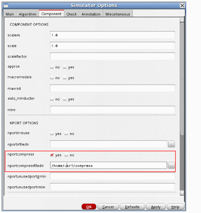
nportunusedportgmin
This option adds resistors to nport pins that are not connected to circuit components. Setting a small value (on the order of 1e-9 to 1e-3) adds a resistor with conductance set to this value from each unconnected pin to ground. This introduces a small error, but adds a small amount of damping to the nport response. This is sometimes useful for obtaining a passive response.
nportunusedportrmin
This option adds resistors in series with nport pins that are shorted together. Setting a small value (on the order of 1e-3 to 1 ohm) adds a resistor with resistance set to this value in series with the connection between pins. This introduces a small error, but adds a small amount of damping to the nport response. This is sometimes useful for obtaining a passive response.
Advanced transient convolution parameters
These properties are provided for S-Parameter simulation experts only.
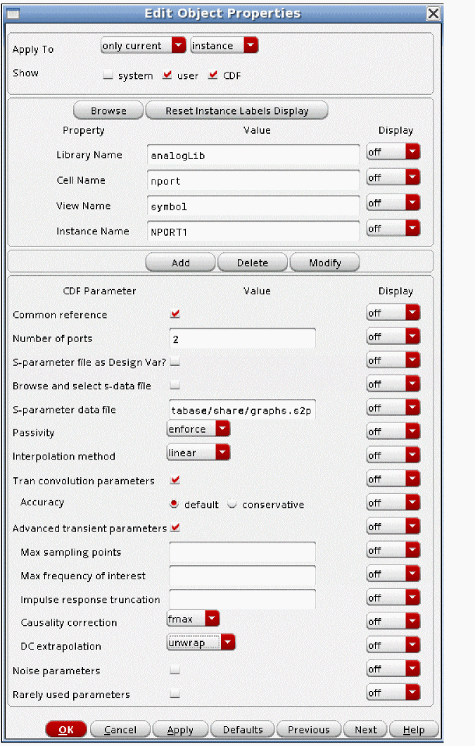
Max sampling points
Max sampling points defines the maximum number of frequency points to be sampled in the adaptive algorithm. The default is 131072. In every case, encountered so far, the actual number of samples taken by the adaptive algorithm is much smaller than the default. In extremely unusual cases, it can be raised to 262144.
Max frequency of interest
The property Max frequency of interest should not be changed unless you are an expert in the simulation of S-Parameter files.
Max frequency of interest (fmax) controls the highest frequency for the frequency domain sampling of the S-Parameter file. Leave this property at the default. The default is three times the highest frequency in the S-Parameter file.
Impulse response truncation
Impulse response truncation is used to deliberately cut off the tail of the impulse response which might theoretically continue to infinite time. Leave this property at the default of 1e-4, which corresponds to a gain of -80 dB.
Causality Correction
The Causality Correction drop-down list contains three choices: no, fmax, or auto. fmax is the default and is highly recommended. Causality enforcement is required in order to have reasonable results from an nport in either the DC or transient-based analyses. Causality correction is performed by setting the transfer function between the highest frequency in the S-Parameter file and three times this frequency so that the data becomes causal. The data within the frequencies specified in the S-Parameter file is unchanged. Setting causality to fmax or auto overrides the setting of the high frequency extrapolation property.
-
no does not add a causality check.
- fmax retains the data in the frequency range of the S-parameter file, and then adds a transfer function above the frequency range in the S-parameter file to force the system to be causal. This transfer function extends to the setting of Max frequency of interest, which defaults to three times the highest frequency in the S-Parameter file. If you suspect that the maximum frequency of interest needs to be changed, use causality Auto instead, if you are not an expert.
- auto applies the causality correction in a similar manner to choosing fmax. auto can also vary the maximum frequency of interest if it needs to get a causal time-domain model.
DC extrapolation
The DC extrapolation can be set to constant or unwrap. constant projects the first point down to zero frequency at exactly the same level. unwrap does an estimation based on the first few frequency points in the S-Parameter file. The default is constant.
Noise Parameters
These properties should never be needed.
Thermal noise
Thermal noise defaults to yes. If you want to disable noise production, set to no.
Thermal noise model
Thermal noise model defaults to external, which reads the noise parameters in the S-parameter file if it is available, and if not, it uses an internal noise model. Internal forces the internal noise model.
Noise correlation
The default is complex. The noise parameters in the S-parameter file might have real and imaginary parts. By default, if these parameters are complex, Spectre observes them. In some cases, passive components may have complex noise parameters in the noise file, which is theoretically not possible. In this case, set Noise correlation to real.
Rarely Used Parameters
These properties should never be needed.
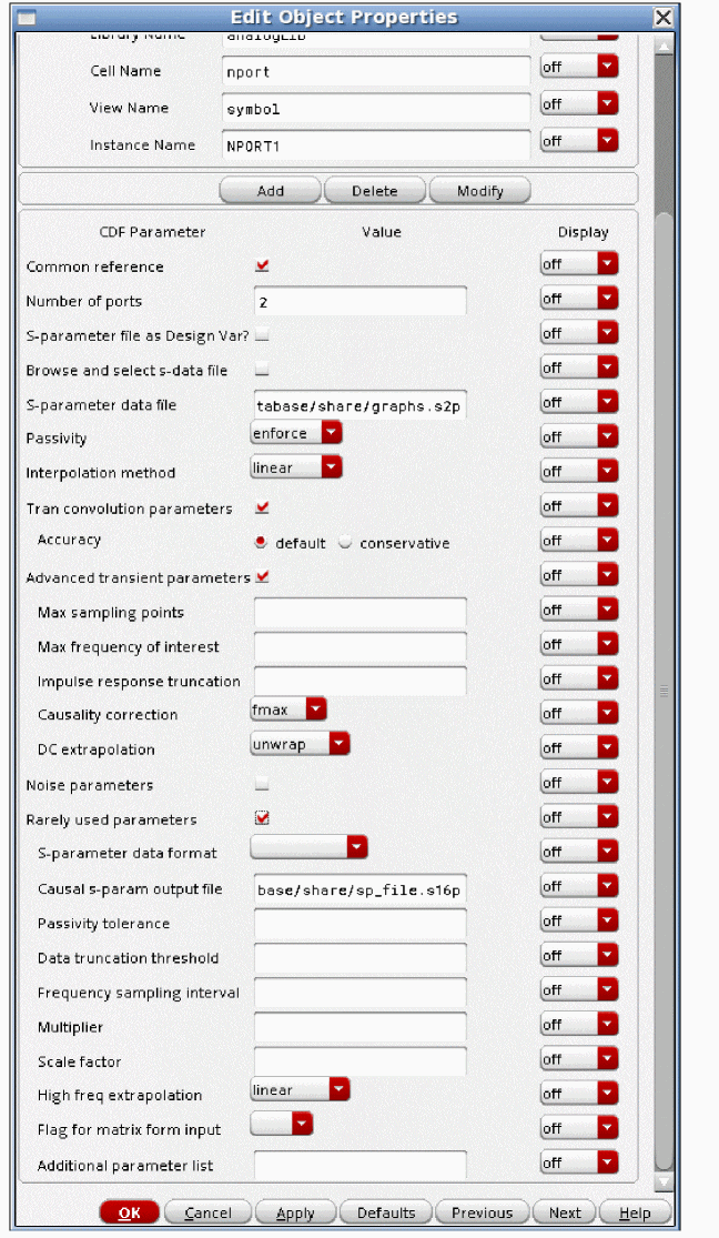
S-Parameter data format
S-Parameter data format is not needed because Spectre can directly parse an S, Y, or Z-parameter file in Spectre, Touchstone1, Touchstone2, CITI file, RFM, or Sigrity BNP format file.
Note that the Touchstone1 file format now provides support for multiple impedances at each port. This is done in the header of the file. When R is listed, then multiple values can be entered up to the maximum number of ports in the file. If a number is omitted, then that number takes on the value of the first R entry.
For example, #GHz RI R 50 1 1 50 means the frequency numbers are in GHz. The data is in real-imaginary format. The resistance is 50 Ohms on port 1 and 4, and 1 Ohm on ports 2 and 3.
#GHz RI R 50 10 20 30 means 50 ohms on port 1, 10 ohms on port 2, 20 ohms on port 3, and 30 ohms on port 4.
#GHz RI R 50 10 means 50 ohms on ports 1, 3and 4, and 10 ohms on port 2.
Causal s-param output file
Enter a filename beginning with slash (/) in this field. Specifying a filename causes the S-Parameter data after causality correction to be placed in this file. This file will be created the first time a tstab or transient simulation runs after the file is specified. This file can then be plotted directly in the waveform display tool. Most of the time, the data within the S-Parameter file frequencies is not disturbed, and the data between the highest frequency and three times the highest frequency is the data that is added to make the time-domain model causal. Below is a comparison of the raw data and the causality-corrected data. The red trace is the original data.
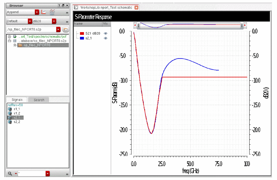
This has the data plotted on a linear X-Axis.
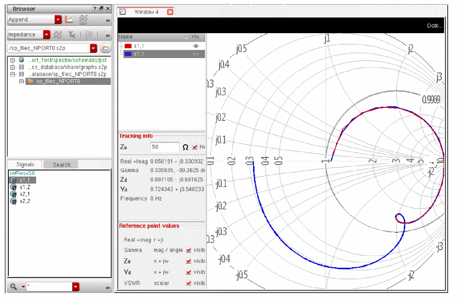
This has the data plotted on the Smith Chart. The original data is in red, and the causality-corrected data is in blue.
Here is the original data in the Smith Chart.
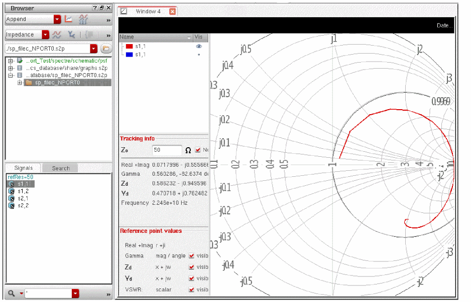
Passivity tolerance
This property is only used when the Passivity property is set to check or enforce. Passivity tolerance does not need to be set. The default is 1e-6. This defines how close to unity gain should be modified by the passivity check and enforcement. Passivity will be enforced and/or reported when the gain is (1 - Passivity tolerance) or greater.
Data truncation threshold
Leave this property at the default of 1e-3, which corresponds to -60dB gain. When the cross coupling terms become smaller than the data truncation threshold, they are ignored. Cross coupling is the coupling from one port to another port.
Frequency sampling interval
Frequency sampling interval sets the delta frequency for the sampling from zero to the maximum frequency of interest. Leave this property at the default value. With adaptive sampling, this should never be necessary. If used, this delta should be a power of two divisor of the maximum frequency of interest.
Multiplier
Multiplier specifies how many nport devices to put in parallel. This is rarely used.
Scale Factor
This scales the frequency of the S-Parameter file. For example, many S-Parameter files have the frequency in GHz. In this case, set the Scale factor to 1e9.
High freq extrapolation
This property should not be used. This property is ignored when causality correction is applied. The High freq extrapolation field can be set to constant or linear. If the causality check is not run, constant maintains the same amplitude and phase as the last point in the S-parameter file to infinite frequency. linear keeps the amplitude constant at the last frequency point, but the phase increases linearly with frequency.
Flag for matrix form input
Flag for matrix form of input should not be needed to be set. In the past, each time the simulation ran, the impulse response was calculated for every port of every instance of the nport every time the simulation was started. In some cases, especially with a large number of ports, this could take considerable time. This flag was provided so the step of calculating the impulse response could be skipped. Since the impulse response is cached and available for re-use at any time, this property should never be needed.
Additional parameter list
This field is typically used by beta customers to unlock new features. Note that when this feature is used, a warning message will be issued. This warning can be ignored.
Controlling Rational Fit Accuracy
Rational fitting is the process of adding multiple poles, zeros, and gain blocks to match the frequency response that is defined in the S-Parameter file. Note that the S-Parameter file may have distributed effects. Approximating these distributed effects with poles and zeros can require a system with a very high order. Matching an arbitrary frequency-domain transfer function with poles and zeros is a difficult and complicated process.
Presently, the best rational fit option is bbspice. No controls are provided for this interpolation method.
At the current time, it is usually better to use the convolution-based algorithms when the interpolation method is set to linear or spline, or use the bbspice rational fitting method.
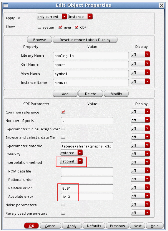
If you do use the rational fit, always test the rational model that is produced by running sp analysis using a circuit composed of an input port, an output port, and an nport with the interpolation method set to rational. Run the sp analysis, and plot all the S-Parameters. Look for differences between the original S-Parameter file and the S-Parameters with the rational fit.
Also, the algorithm is known to take a very long time to run for S-Parameter files with a large number of ports.
The nport component has three parameters to control the accuracy of the rational interpolation process:
- relerr (The Relative error field)
- abserr (The Absolute error field)
- ratorder (The Rational order field)
You can use these parameters to trade off accuracy against model size and simulation time. In general, the more stringent the accuracy requirement, the higher the model order. Higher-order models require longer extraction and simulation time. SpectreRF can automatically generate a model that meets a specified accuracy requirement. You can also specify the model order directly to SpectreRF.
Using the relerr and abserr Parameters
The relerr parameter is used to control the accuracy of the rational fit when the gain is larger than the gain specified in abserr. Usually, relerr is on the order of about 0.01, which sets a 1% error in the rational fit when the gain is large. Usually, abserr is in the order of 1e-3 to 1e-4, which specifies that when the gain is less than abserr, allow a lot of error in the rational fit. 1e-3 is -60dB gain, and 1e-4 is -80 dB gain. The abserr parameter lowers the order of the model by allowing fewer poles and zeros when the gain is small.
Consider the data shown by the solid line in Figure 9-19. In this example:
If you are not interested in the details of the filter behavior in the stopband, you can set abserr to the level shown and these details are ignored in the interpolation.
Figure 9-19 Using relerr and abserr
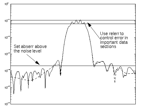
This example has approximately a 10% ripple in the passband. To ensure adequate error control there, set relerr to much less than 0.1, for example, 0.01.
The dashed line in Figure 9-19 shows an interpolation function with the error control levels specified in Figure 9-19: abserr=2e-4, and relerr=0.01. Details of the data below the abserr threshold are not resolved by the rational interpolation.
To recover the details in the stopband, set abserr to about 1e-5 for this example.
If there is noise in the data, set relerr and abserr above the respective noise levels. Otherwise, Spectre and SpectreRF attempt to interpolate the noise, resulting in very high order models and very long simulation times.
Remember that if you set relerr to zero, then, from the formula above, pure absolute error is used. Conversely, if you set abserr to zero, the error control is based solely on the errors relative to the magnitude of the input data.
Using the rational order (ratorder) Parameter
In general, it is usually best to specify only the accuracy parameters, relerr and abserr, and to let SpectreRF automatically select rational order, the order of the rational approximation. However, if you have information about your data set, you can direct SpectreRF to use a specific order of approximation in the rational interpolation. For example, if you know that your tabulated S-parameter data represents a sixth-order filter, you might instruct SpectreRF to use a seventh or eighth order fit. The slightly higher order gives SpectreRF flexibility to adjust for any noise or non-ideal behavior in the data.
When you specify the ratorder parameter, SpectreRF tries to meet the error requirements specified by relerr and abserr, but is limited to the number of poles and zeros it can use to achieve them. If the error specified cannot be achieved with the number of poles and zeros you have specified, a warning message is generated to let you know that the error requirements were not met.
ROM data file
If this file is specified, when the rational fit is performed, the results of the rational fit are stored in the specified file as a Spectre format reduced order model.
Troubleshooting
Certain S-parameter data sets might cause difficulty for the rational interpolation process. Types of data to avoid are:
- Data specified only over a very narrow frequency range. Time-domain simulation requires time-domain models with a wider range of values; values that lie outside the narrow frequency range. Data extrapolation might be difficult and is always risky.
- Very noisy data. Noisy data might lead to large, unreliable time-domain models.
- Data on a very sparse frequency grid. Accurate interpolation of such data might be impossible.
- Data with long ideal delays.
- Data representing idealized lossless elements, such as lossless transmission lines.
Assessing the Quality of the Rational Interpolation
If you suspect a problem with the rational interpolation process, you can investigate it using the sp analysis using the following steps:
- Construct a test schematic consisting of an nport component with interpolation set to rational, as discussed in “Using the nport Component”.
-
Next add the appropriate number of port components to the schematic. An example with two ports is shown below.
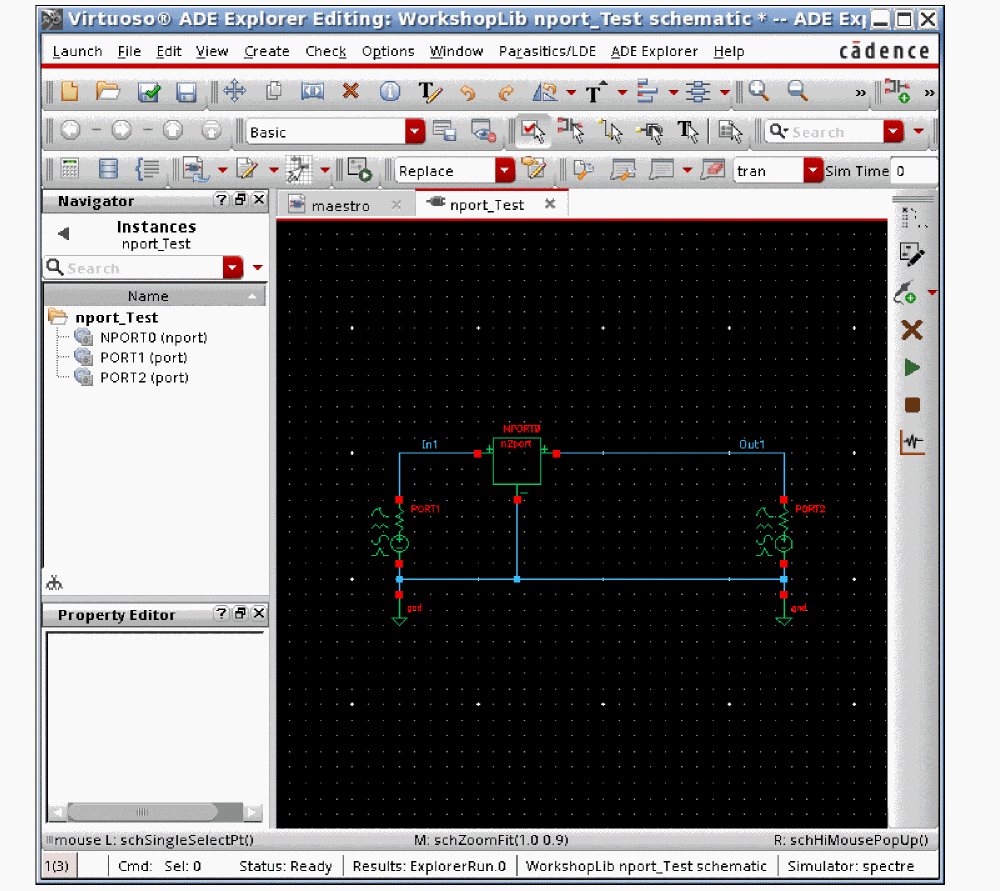
-
Perform an sp analysis on the nport component and look for anomalies.
Large swings in interpolated values and S-parameter magnitudes greater than one both suggest a problem.
Large changes in the interpolated data result from an inaccurate fit. Usually, when this happens, there are local peaks or suckouts in the S-Parameter data.
S-parameter values greater than one result from a non-passive (energy-generating) model that might create unstable time-domain solutions. Be particularly critical of anomalies near the zero frequency (DC). Most S-Parameter files do not have zero frequency data, so the DC point must be extrapolated. Sometimes in rational fit, the DC point can be inaccurate.
When the anomalous behavior occurs within the frequency range of the data in the S-parameter data file, it usually indicates an inaccurate rational interpolation. Anomalous behavior below the first frequency point and above the last frequency point are uncommon, but always needs to be checked. If you have this anomalous behavior, linear interpolation is suggested.
Possible Problems with Rational Fit
Because the rational fit can have unexpected behavior, it is suggested that you run an S-Parameter simulation over a very wide frequency range. Check for those behaviors in the sp analysis.
A comparison between rational and linear interpolation is shown below. Note that S21 and S11 both go considerably above unity gain (0dB) above about 60GHz for the rational fit. The data in this file stops at 25GHz. This data is from a passive structure.
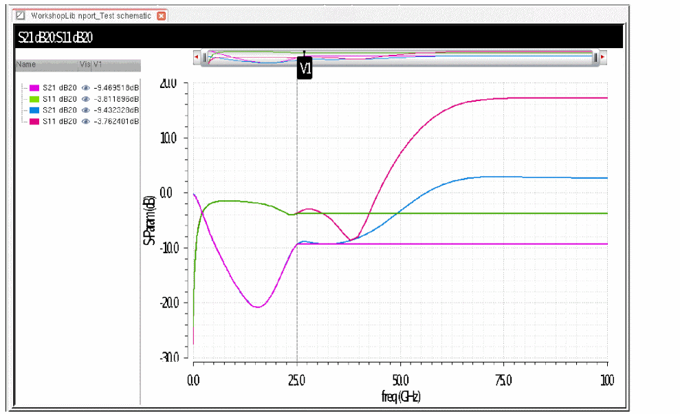
Magenta and green are the original data. Blue and red are the rational fit.
Also note the differences in the low frequency data shown below.
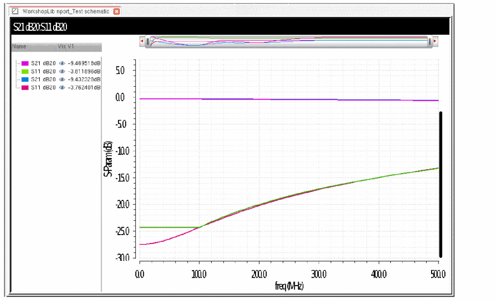
- Verify that all the conditions listed at the beginning of the Troubleshooting section are met.
- Try decreasing relerr or abserr or both.
- Try specifying a higher-order interpolation with the ratorder parameter.
- Remember that measured data can contain fine details that might require a higher order than you might expect from a casual inspection of the data.
- If the anomalous behavior occurs outside the tabulated frequency range, try changing the abserr, relerr, or ratorder parameters. Sometimes anomalies can be removed by using a more accurate fit. However, there are limits to the ability to extrapolate outside the frequency interval you specify. You might need to specify additional data points in the S-Parameter file to fix the problem.
Difficulty can also sometimes be seen in running the transient analysis. Below is a Choosing Analyses form that shows a setup to run the transient to 10nsec.
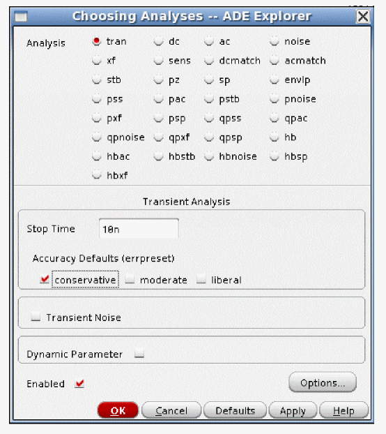
The simulation runs, and the data plots, but note that only part of the waveform has been calculated.
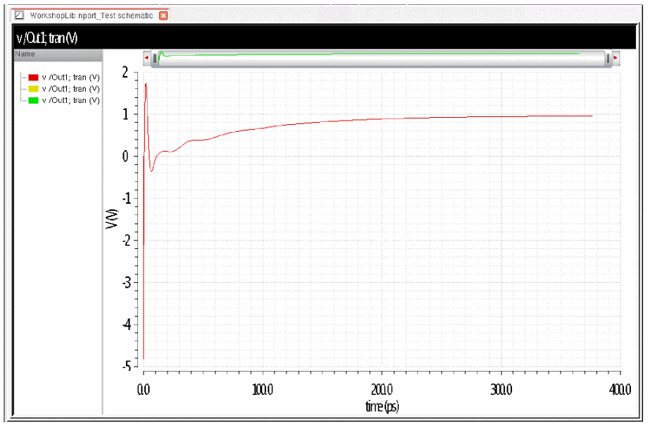
When you look in the Spectre output log, the iterations have stopped because the solution goes above 1GigaVolt.
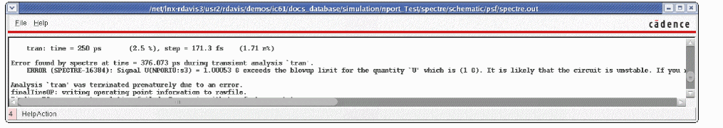
Model Reuse
Rational Fit
When rational or bbspice is set for the interpolation method, Spectre caches the rational model in the simulation directory. As long as you do not change the S-Parameter file, the rational fit will be reused.
Linear and Spline Fit
Prior to MMSIM 12.1, every instance of every nport calculated the impulse response at the beginning of the simulation. In some cases, this added a lot of time in order to accomplish this. Starting with MMSIM 12.1, only the impulse responses that need to be calculated are performed. For example, if there are multiple instances of nport with the same S-Parameter file and the same nport settings, the impulse response is calculated only once.
The impulse response data is cached by default so that as long as the S-Parameter data and the properties on the nport do not change, the cached data is reused in subsequent simulations. When the properties on the nport instance are modified, then a new impulse response is needed. The impulse response is recalculated and cached without eliminating the original cached data file. This is done so that if you go back to the original settings, you do not need to re-run the impulse response.
Additionally, file locking has been implemented to allow multiple users to have access to a shared impulse response directory. This is controlled by the nportfiledir option described below.
There are two options that control caching. These options are located in the ADE Explorer options located in Simulation-Options-Analog.
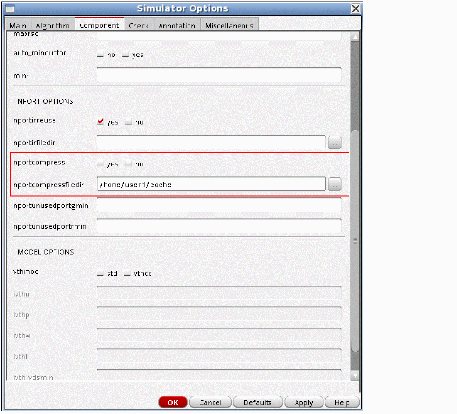
Nportirreuse
This option has the default of yes. Keep this at the default to save time. This option enables caching of the impulse response.
nportirfiledir
This controls the location of the cached impulse response files. The default (blank) sets the location to /home/<username>/.cadence/mmsim. When a directory name is specified in the nportirfiledir option, the impulse response files are cached in the specified directory. This can be a shared directory between users, as long as all the users have write permissions in that directory.
Dcblock, dcfeed, indq, and capq
Ideal components are provided to allow what-if analysis without needing details of specific structures to allow the determination of what is needed to meet the specifications.
These components are provided for any analysis in Spectre except shooting. This allows the use of inductors and capacitors with Q in s-parameter, ac, and hbac analyses, along with the other small-signal Spectre and SpectreRF analyses.
Dcfeed
Dcfeed is an ideal short at DC and an ideal open at all other frequencies. For the shooting PSS and the transient analyses, dcfeed is an inductor with a default value of 1uh.
The symbol and the properties form are shown below. The Model Name field should be left blank.
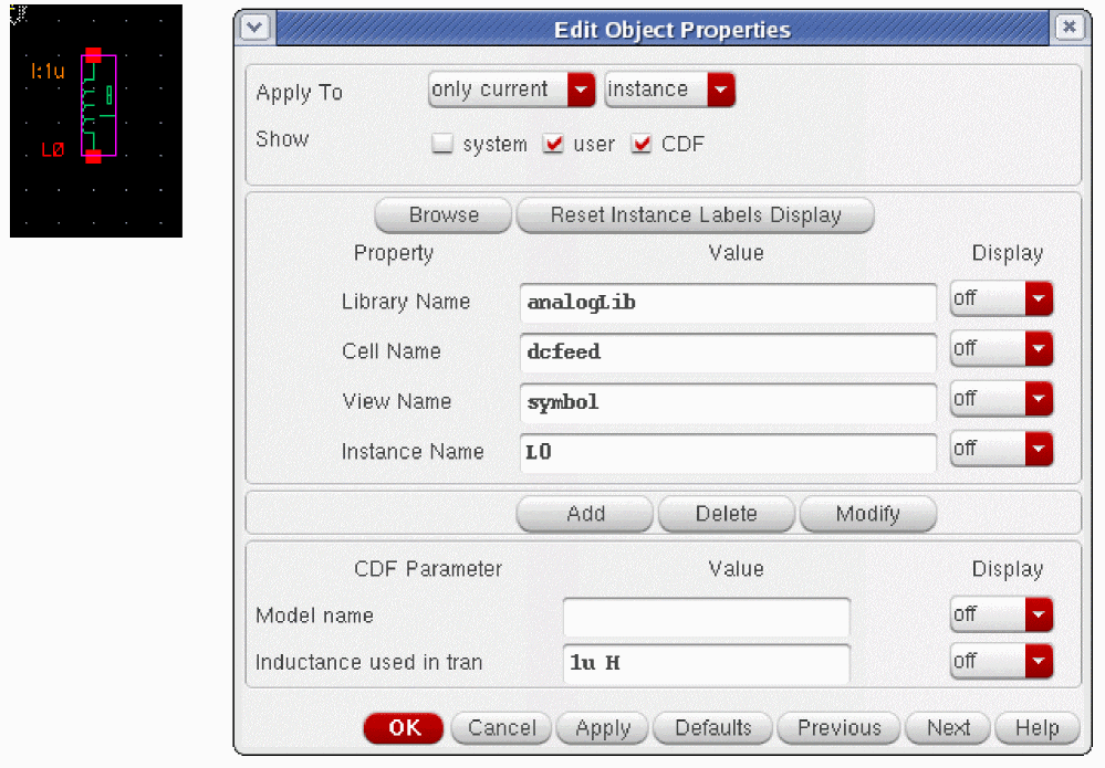
An example comparing the dcfeed, and inductor, and a wire is shown below.
This example shows three cascode amplifiers with different connections to the power supply for the upper transistor. The left amplifier has a dcfeed. The center amplifier has an inductor. The right amplifier has a wire. In the amplifiers above, the resistor to the left has the output point set to 1K ohm.
When the inductor and the dcfeed are essentially open, the gain of the circuit is set by the resistor. When the impedance is less than 1Kohms, the load impedance is dominated by the impedance of the DCfeed or inductor. In this way, we can deduce what is happening at low frequency by running a simulation.
The amplitude of the input is deliberately large so the amplifiers tend toward the mixer behavior. The input signals are at 2.45GHz and 2.451GHz. The difference frequency is 1MHz. The 1 MHz signal will be analyzed so the behavior of the dcfeed, inductor, and wire can be evaluated.
At all frequencies other than DC, the dcfeed is open. The inductor impedance goes up with frequency. At 1MHz, the impedance of the 1uh inductor is 6.28 ohms.
Below is the simulation result from harmonic balance near 2.45GHz. The result agrees for the dcfeed and inductor. With a wire, essentially no signal is present.
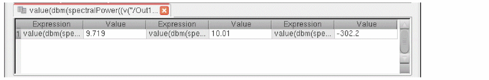
In the table above, the left result is the output signal level in dBm for the amplifier with the dcfeed, the middle is the signal level in dBm for the amplifier with the inductor, and the right is the output signal level in dBm for a wire connected to the power supply. The third output is at the numerical noise floor of the simulation.
Below is the spectral plot near 2.4GHz.
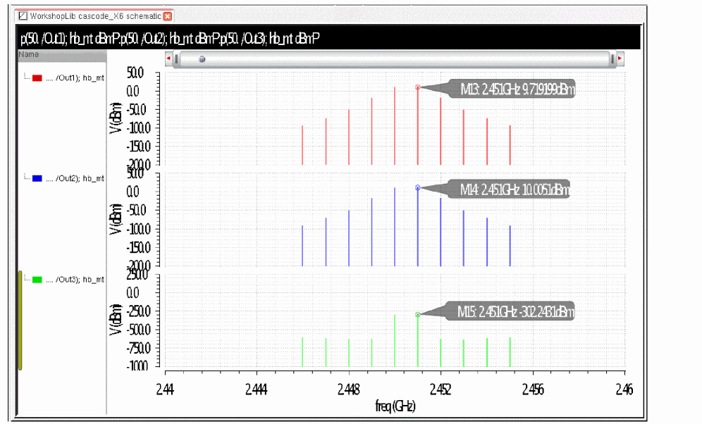
Below is the simulation result near 1MHz.
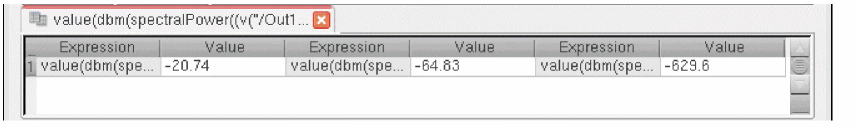
In the table above, the left result comes from the amplifier with the dcfeed. The center is with the inductor, and the right is with the wire. The dcfeed is open at 1MHz, so the signal level is set by the 1K resistor. Because the inductor has an impedance of only 6.28 ohms at 1MHz, the signal is much smaller than for the dcdfeed. With a wire, you see the numerical noise floor of the simulation.
The spectral plot is shown below.
Dcblock
Dcblock is a near open (1Gohm) at DC and an ideal short at all other frequencies. For the shooting PSS and the transient analyses, dcfeed is a capacitor with a default value of 1uF.
The schematic symbol and properties list are shown below.
Below is an example with three cascode amplifiers that use different connections to the output load resistor. The left amplifier has a dcblock in series with the load resistor. The middle amplifier has a capacitor in series with the load resistor. The amplifier on the right has a wire connected to the load resistor. The output resistance is 10KOhms.
Here is a table with the DC values from the three cases. The left column is the DC voltage on the load resistor with the dcblock, the center column is the DC voltage with the capacitor, and the right column is the DC voltage with the wire.
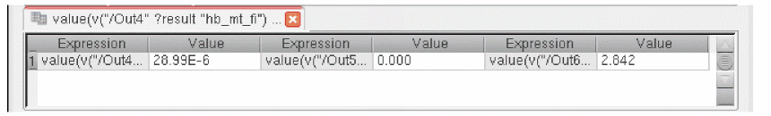
The voltage with the dcblock is only a few microvolts. This is because it is a 1Gohm resistor at DC. The capacitor is a perfect open at DC, so the voltage is exactly zero. With a wire, the DC bias level appears at the load resistor.
Here, is the simulation results from harmonic balance. Instead of dB, the vertical axis is linear volts. Note that the DC level is small for the dcblock. This is the top trace. The dcblock is a 1e9 ohm resistor at dc, and an ideal short at all non-zero frequencies. The center trace is from the amplifier with the capacitor, and the bottom trace is from the circuit with the wire.
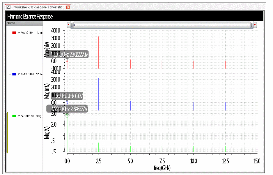
indq
Indq is a series inductor and resistor. There are three different modes with different frequency behavior in each mode. Below is the test circuit for the plots that will come later. PORT1 is defined as port1 in a single port S-parameter analysis so that the Z-Parameters for the inductor can be directly plotted.
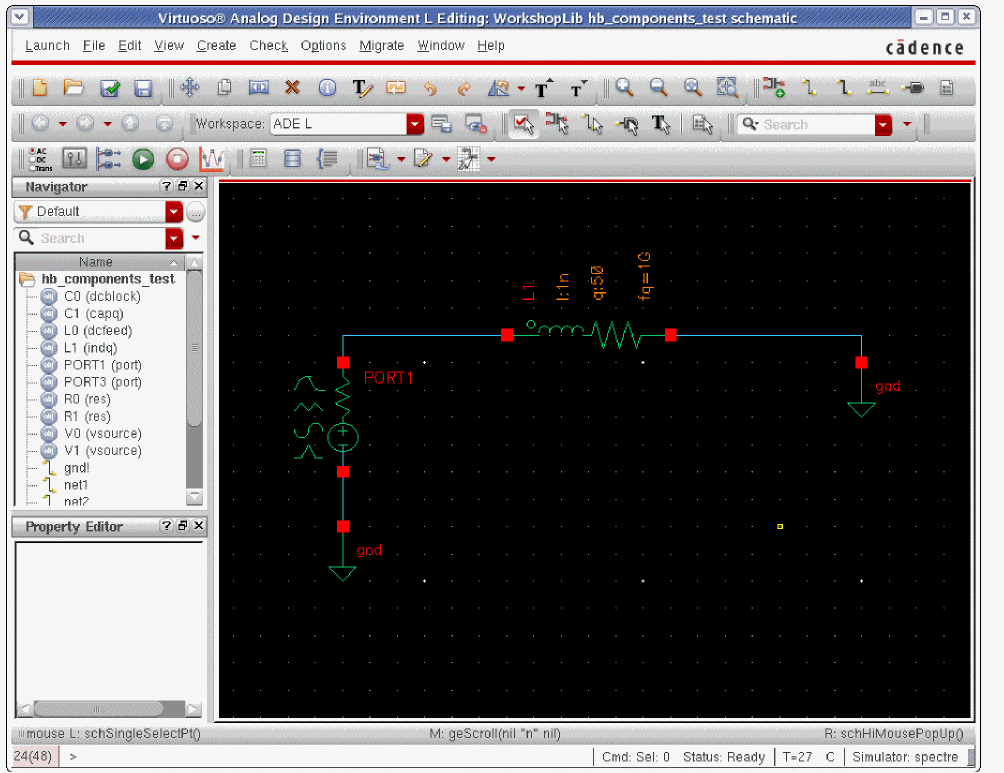
The properties list for mode 1 is shown below.
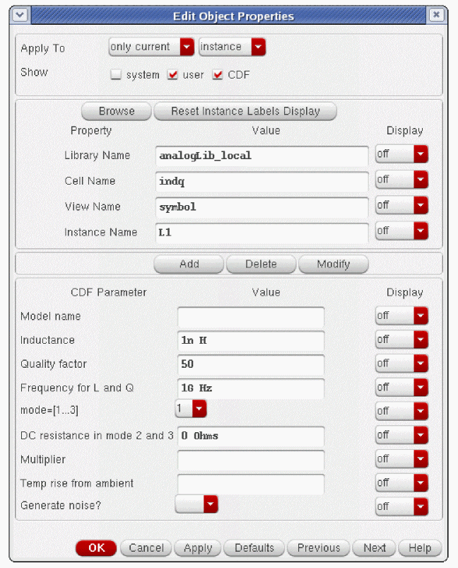
The inductor with Q works in all the analyses except for shooting.
The indq component has three modes, with different behavior in each mode. For all three modes, you need to specify the inductance, Q, and the frequency for the inductance and Q specification.
Mode 1
In this mode, the indq model is a series RL branch with R=constant and L=constant at the value given by the Inductance property. The value of the property Rdc in mode2 and 3 is not used in this mode.
Special case: specifying Q=0 or F=0 makes the indq component just an inductor with the value L without any series resistance.
The resistance is calculated as follows:
Below is a plot of the inductance, resistance, and Q with respect to frequency. A vertical marker has been placed at 1GHz, which is the frequency for L and Q. The inductance and resistance are constant, and the Q rises with frequency.
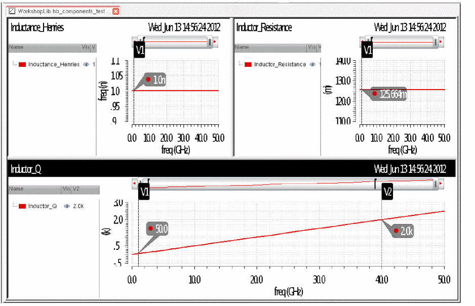
Mode 2
In this mode, both the resistance and the inductance are frequency dependent.
If RDC in mode 2 and 3 property is set to zero or is left blank, the DC resistance is 0.05*the resistor value that is set at the frequency defined by the Frequency for L and Q property.
RDC, R'', and ![]() being constants are the classic forms of the skin-effect expressions for the resistance (grows as the square root of frequency) and inductance (the internal inductance decays inversely proportional to the square root of frequency). These expressions specify a causal frequency dependence of impedance. At the frequency specified in the Frequency for L and Q property, L and Q are equal to the values specified for Inductance and Quality factor.
being constants are the classic forms of the skin-effect expressions for the resistance (grows as the square root of frequency) and inductance (the internal inductance decays inversely proportional to the square root of frequency). These expressions specify a causal frequency dependence of impedance. At the frequency specified in the Frequency for L and Q property, L and Q are equal to the values specified for Inductance and Quality factor.
The transient analysis cannot use frequency-dependent impedances, so it uses the inductance specified in the properties form, and the RDC in Mode 2 and 3 property for the resistance.
Below is the property form for mode 2.
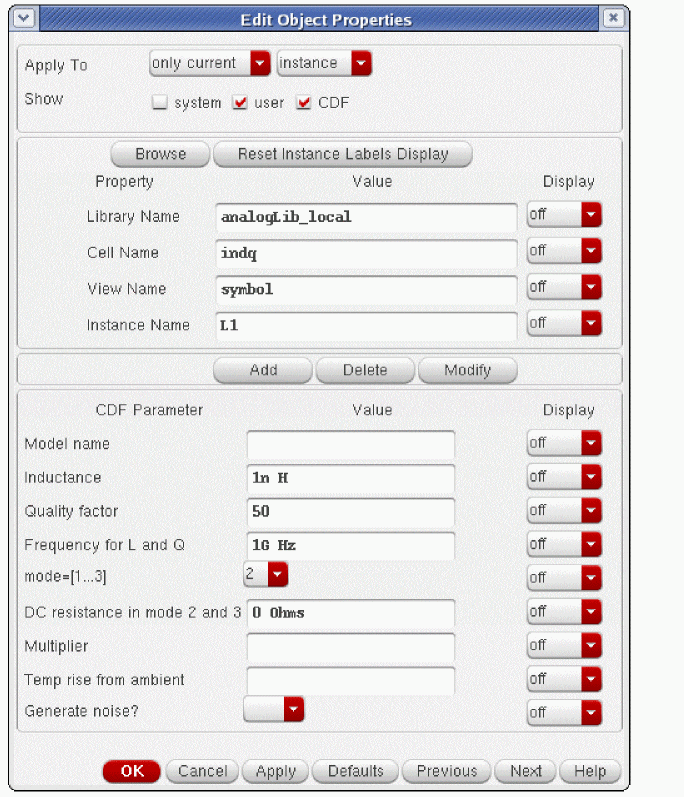
Below is the inductance, resistance, and Q. Note the log frequency for inductance.
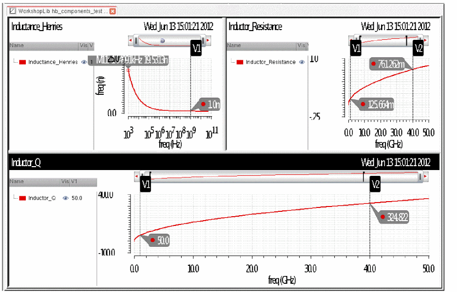
Mode 3
The advantage of mode 3 is that the non-physical frequency dependence of R near f=0 (DC) present with mode=2 is corrected. In this mode, R(f) has a reasonable frequency derivative near f=0. However, the expressions are non-causal as R varies as a function of frequency while L remains constant.
In this mode, L is constant at the value specified and
If the RDC in mode 2 and 3 property is set to zero, the DC resistance is 0.05*the resistor value that is set at the frequency defined by the Frequency for L and Q property.
Because the transient analysis cannot handle frequency-dependent resistance, the transient analysis uses the inductance specified in the properties form, and RDC for the resistance.
The properties list for mode 3 is shown below.
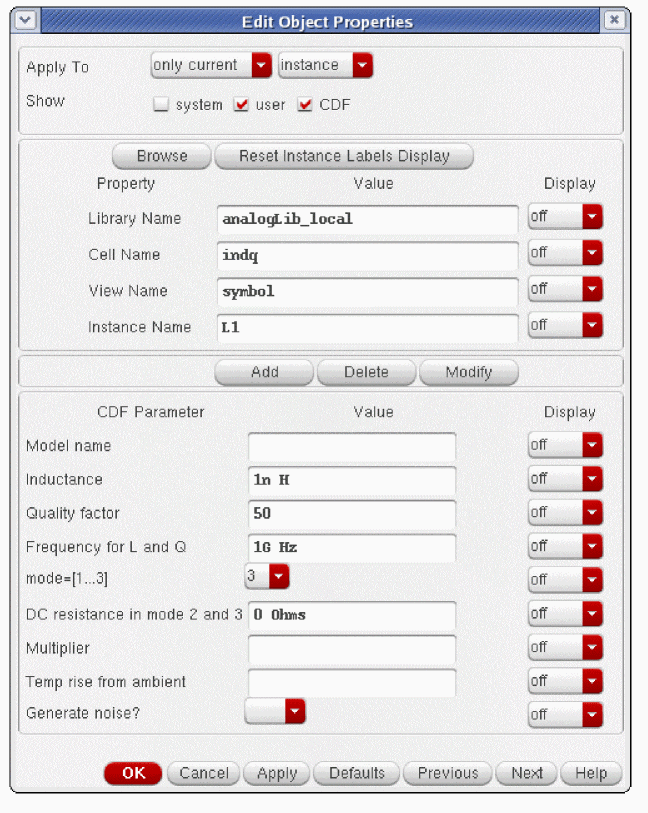
The inductance, resistance, and Q in mode 3 are plotted versus frequency, as shown below.
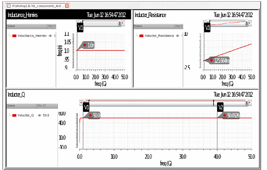
Here is an expanded view of Q at low frequency. Q drops off at low frequency.
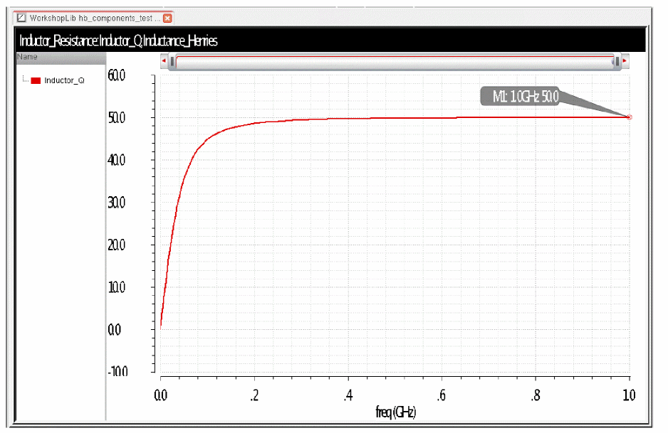
capq
Capq is a parallel capacitor and resistor. There are three different modes with different behavior in each mode. In all three modes, the capacitor is constant at the value specified in the properties form. Below is the test circuit for the plots that will come later. PORT1 is defined as port1 in a single port S-parameter analysis so that the Y-Parameters for the capacitor can be directly plotted.
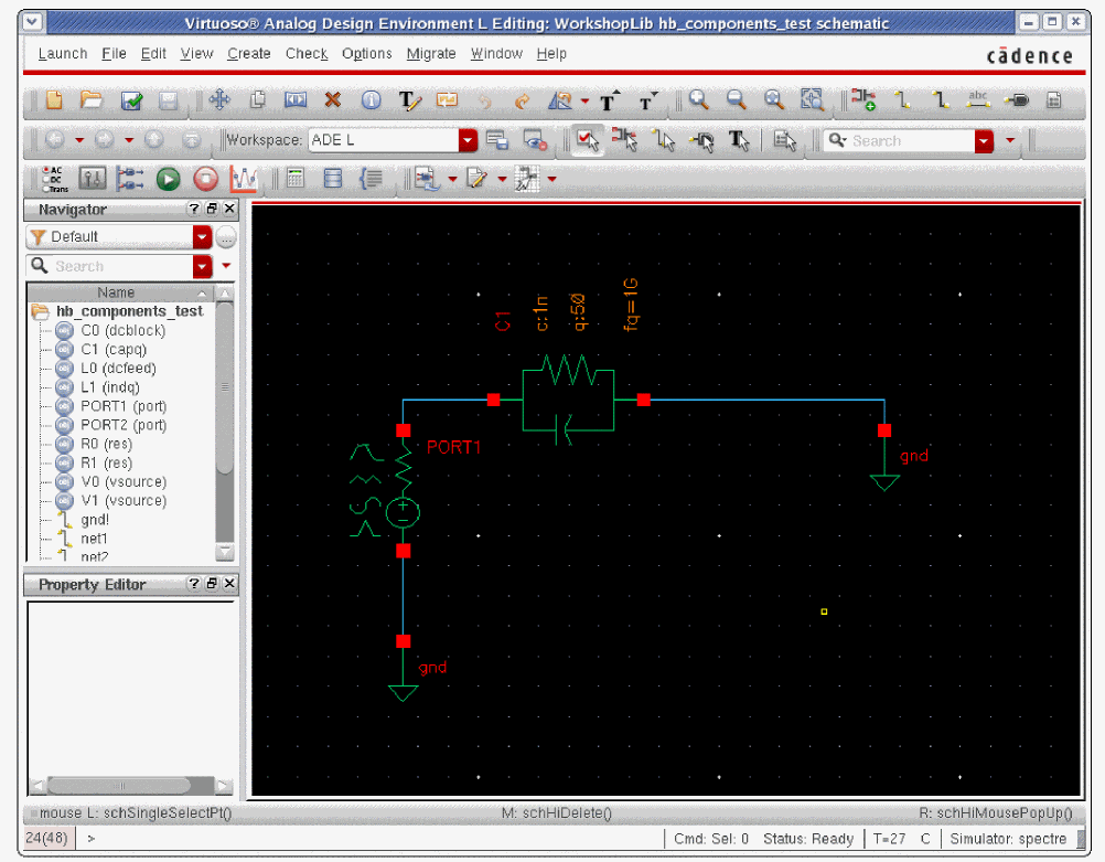
Mode 1
In this mode, the capq model is a parallel R C branch with R=constant and C=constant at the value given by the Capacitance property.
The conductance is constant as given below.
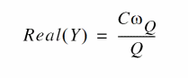
![]() above is the frequency for the Q value in radians per second.
above is the frequency for the Q value in radians per second.
This model is used in all the analyses, except shooting, where it is not supported.
Below is the properties list for the capq with mode 1 selected.
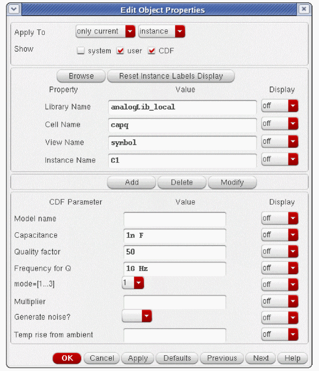
Below is a plot of the conductance, and Q with respect to frequency in mode 1. A vertical marker has been placed at 1GHz, which is the frequency for Q. The capacitance and resistance is constant, and the Q rises linearly with frequency.
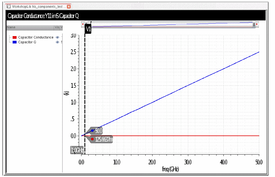
Mode 2
In mode 2, the conductance is frequency dependent as shown in the equation below.
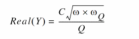
The capacitance is constant in all modes.
![]() above is the frequency where Q is specified in radians per second.
above is the frequency where Q is specified in radians per second.
Mode 2 is non-causal. Because the resistance is frequency dependent, the transient analysis uses the capacitance specified in the properties list with no resistor in parallel.
Below is the properties form for mode 2.
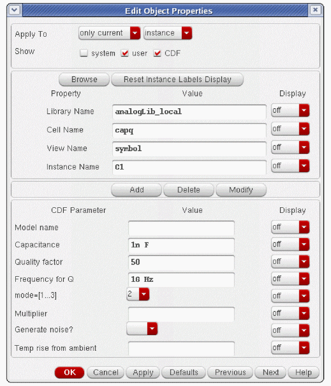
Below is the conductance and Q versus frequency. Vertical markers have been placed at 1GHz and 40GHz. Mode 2 is a compromise between a linear Q increase with frequency in mode 1, and a constant Q in mode 3. The Q goes up with frequency, but not as fast as in mode 1.
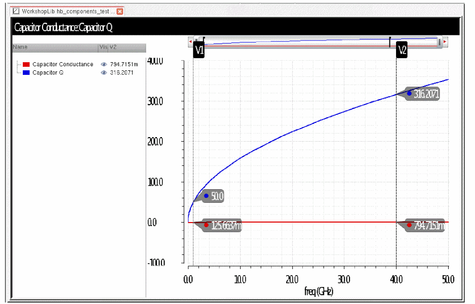
Mode 3
In mode 3, C is constant at the value specified in the properties form, and the conductance is
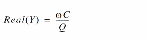
Mode 3 is non-causal. Because the resistance is a function of frequency, the transient analysis uses just the capacitance term.
The properties list for mode 3 is shown below.

The conductance and Q versus frequency is plotted below.
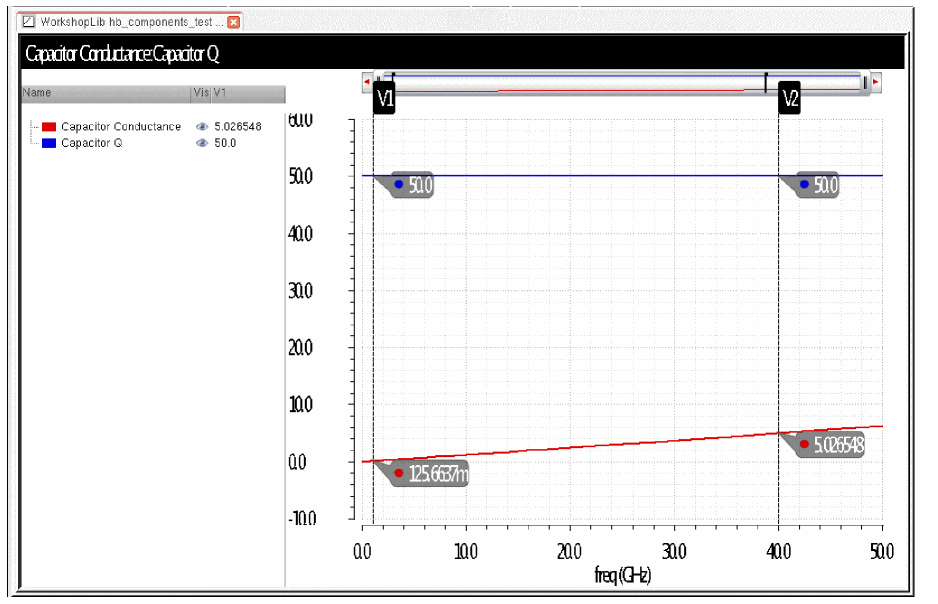
In mode 3, the capacitance is constant, and the Q is constant. The resistance is a function of frequency.
Reference: S-Parameter Equations
This section describes the equations used by the VIVA Calculator to plot data generated by Spectre S-parameter simulations.
Using the VIVA Calculator in the Analog Design Environment, you can plot the following S-parameter data:
- Network Parameters
- Two-Port Scalar Quantities
- Two-Port Gain Quantities
- Two-Port Network Circles
- Equation for VSWR (Voltage Standing Wave Ratio)
- Equation for GD (group delay)
Use the buttons located in the Function area of the S-parameter Direct Plot Form to specify the type of data to plot.
Network Parameters
You can plot S, Y, Z, and H network parameters.
S-parameters, Y-parameters, and Z-parameters (denoted as SP, YP, and ZP on the Direct Plot Form) are defined for circuits with any number of ports. H-parameters (denoted as HP on the Direct Plot Form) are defined only for two-port circuits.
You can plot parameters on polar charts, Smith charts, or on rectangular plots after applying a Modifier option. The dB conversion uses
Equations for Network Parameters
For the ZP, YP, and HP parameters, Spectre returns S-parameters to the analog design environment. The environment converts them, as needed, to the equivalent Z, Y, and H matrixes using standard published methods. Spectre calculates S-parameter values.
SP (S-parameter) values are calculated by Spectre.
The Z-parameter equation is as follows:
-
S m is the N-port S-parameter matrix -
I is the N x N identity matrix -
Z ref is the characteristic impedance of the port -
Z m is the resulting Z-parameter matrix
YP (Y-parameter) equations
The Y-parameter equations are as follows:
-
S m is the N-port S-parameter matrix -
I is the N x N identity matrix -
Y ref is a diagonal matrix defined as
The HP (H-parameter) equations
The HP (H-parameter) equations only apply to two-port circuits.
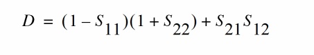
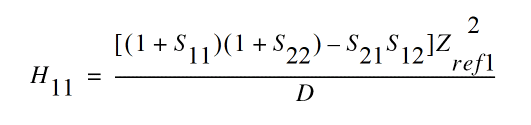
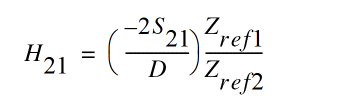
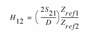
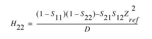
Two-Port Scalar Quantities
The two-port scalar quantities include
-
NF min is minimum noise figure -
NF is noise figure -
R n is equivalent noise resistance -
G min is Optimum Noise reflection coefficient -
B 1f is alternative stability factor -
K f is stability factor
You can plot two-port scalar quantities only against frequency. In addition, you can plot them only on rectangular charts. Figure 9-20 illustrates a generic two-port circuit that defines impedances and reflection coefficients.
Figure 9-20 A Generic Two-Port Circuit
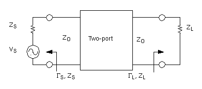
-
Z s is the source impedance - Γs is the input reflection coefficient
-
Z L is the load impedance - ΓL is the load reflection coefficient
-
Z O is the characteristic impedance
Equations for Two-Port Scalar Quantities
Gmin (Optimum Noise Reflection Coefficient) Equation
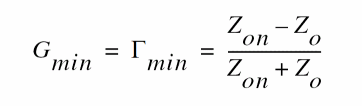
-
Z o is the characteristic impedance -
Z on is the source impedance associated with minimum noise figure (NF min)
NFmin (Minimum Noise Figure) and NF (Noise Figure) Equations
The
Plot noise figure (NF) in dB by setting Modifier to dB10
Use
The
The
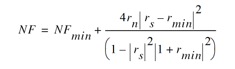
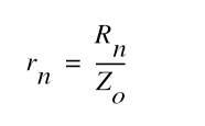
Here
Rn (equivalent noise resistance)
Rn plots equivalent noise resistance. The
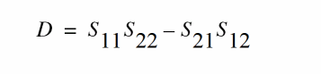
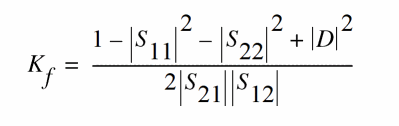
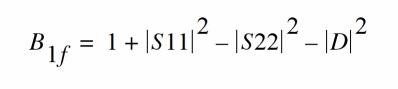
Two-Port Gain Quantities
The following gain quantities are valid only for two-port circuits:
-
G A(available gain) is the power gain obtained by optimally matching the output of the network. -
G P(power gain) is the power gain obtained by optimally matching the input of the network. -
G T (transducer gain) shows the insertion effect of a two-port circuit. This quantity is used in amplifier design. -
G umx (maximum unilateral transducer power gain) -
Gmax (maximum available gain) sho
ws the transducer power gain when there exists a simultaneous conjugate match at both ports. -
G msg (maximum stable gain) shows the gain that can be achieved by resistively loading the two-port such thatk = 1 and then simultaneously conjugately matching the input and output ports. For conditionally stable two-ports, you can approach the maximum stable gain as you reduce the input and output mismatch. If you attempt a simultaneous conjugate match andk < 1, the two-port oscillates.
Equations for Two-Port Gain Calculations
GA (Available Gain) Equations
Available gain equations for output conjugately matched.
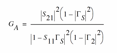
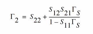
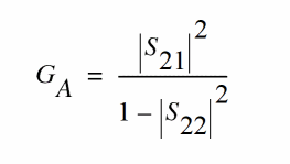
To plot
GP (Power Gain) Equations
Power gain equations for input conjugately matched.
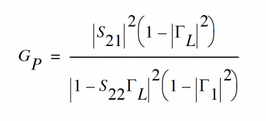
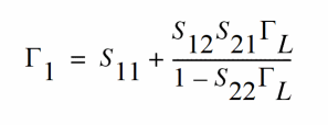
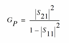
To plot
GT (Transducer Gain) Equations
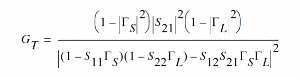
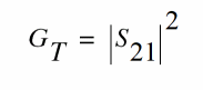
Using the calculator, you can plot
Gmax (Maximum Available Gain) Equations
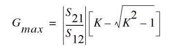
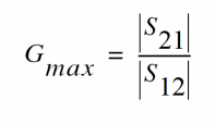
Gumx (Maximum Unilateral Transducer Power Gain) Equation
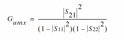
Gmsg (Maximum Stable Power Gain) Equation
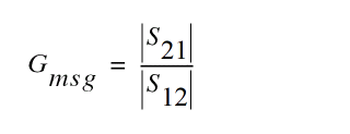
Mu Equation
Mu returns the geometrically derived stability factor for load. This measurement gives the distance from the center of the Smith chart to the nearest output (load) stability circle. This stability factor is given by:
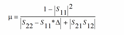
Here, Delta is the determinant of the S-parameter matrix. Having mu > 1 is the only mandatory and sufficient condition for unconditional stability of the two-port network.
Mu' Equation
Mu' (mu_prime) returns the geometrically derived stability factor for source. This measurement gives the distance from the center of the Smith chart to the nearest unstable-input (source) stability circle. This stability factor is given by:
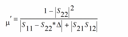
Here, Delta is the determinant of the S-parameter matrix. Having mu_prime > 1 is the only mandatory and sufficient condition for unconditional stability of the two-port network.
The mu test is a test for unconditional stability and the magnitude of mu is a measure of the stability. That is, if one two-port has a larger mu, it is more stable.
The advantage of the mu test is that only a single parameter needs to be evaluated. There are no auxiliary conditions like the K, B1 test (based on Rollett's and Kurakawa's derivations).
Two-Port Network Circles
NC plots constant noise contours at the input of a two-port circuit. GAC plots constant gain contours at the input port, and GPC plots constant gain contours at the output port. Gain contour values reflect an optimum match at the opposing port.
Noise and Gain circles can be plotted at a single dB value for a range of frequencies or at a single frequency for a range of dB values. If you do not enter values for the frequency range, a circle is plotted for every simulated frequency for which a circle with the specified value exists.
SSB plots stability circles at the input port, and LSB plots stability circles at the output port. You can also specify a limited frequency range for these contours.
Equations for Two-Port Network Circle
NC (Noise Circle) Equations
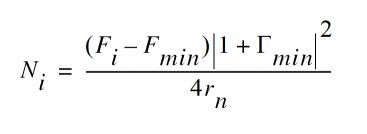
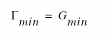
The center is calculated using
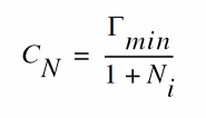
The radius is calculated using
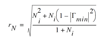
GAC (Available Gain Circle) Equations
The center is calculated using
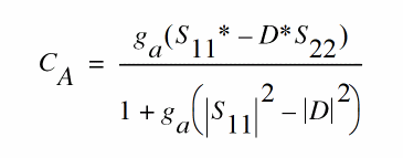
The radius is calculated using
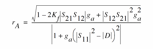
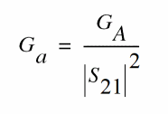
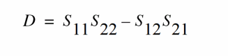
GPC (Power Gain Circle) Equations
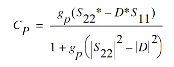
The radius is calculated using
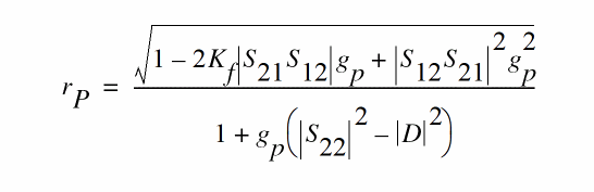
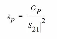
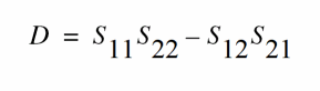
LSB (Load Stability Circle) Equations
The center is calculated using
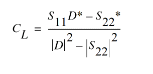
The radius is calculated using
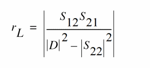
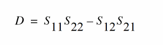
SSB (Source Stability Circle) Equations
The center is calculated using
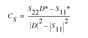
The radius is calculated using
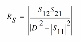
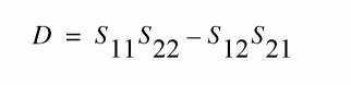
Equation for VSWR (Voltage Standing Wave Ratio)
VSWR is calculated from the S-parameters. You can plot the VSWR at any port in the circuit on a rectangular chart.
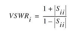
Equation for ZM (Input Impedance)
You can plot input impedance if all other ports are matched.
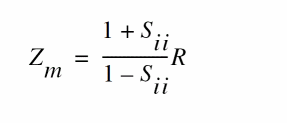
Where R the reference impedance of the port of interest and i
Equation for GD (group delay)
GD (group delay) approximates the derivative of the phase with respect to frequency, normalized to 360 degrees. Units for group delay are in seconds.
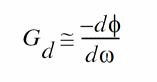
Group delay is calculated from the phase of the corresponding S-parameter (for example,
References
To learn the technical details about how SpectreRF converts S-parameter data to a time-domain description, see the article “Robust rational function approximation algorithm for model generation,” by C. P. Coelho, J. R. Phillips, and L. M. Silveira. This article appeared in the proceedings of the 36th Design Automation Conference, New Orleans, LA, June 1999.
Return to top