BSIM-IMG Model Equations
Bias Independent Calculations
Physical Constants
Physical quantities in BSIM-IMG are in M.K.S units, unless specified otherwise.
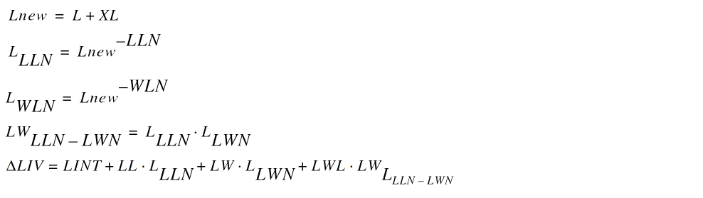
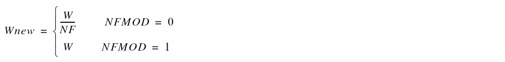
Effective Channel Width, Channel Length
Binning Calculations

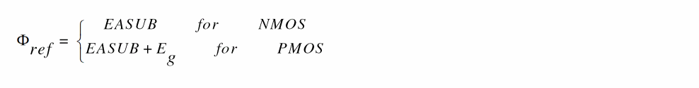
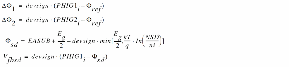
Front and Back Gate Workfunction Calculation
Terminal Voltages and Pre-Conditioning
Terminal Voltages and Vdsx Calculation
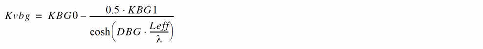
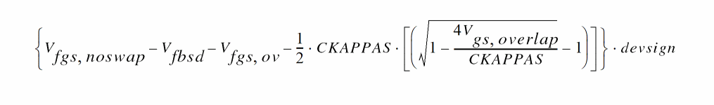
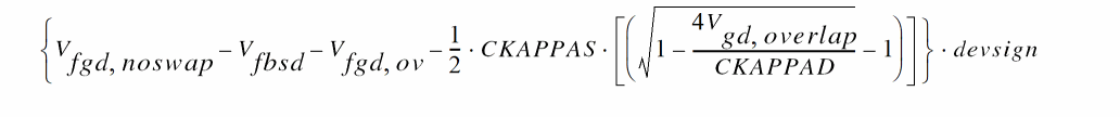
Back Gate Biasing Effect

Short Channel Effects
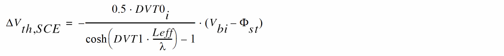
Vt Roll-off
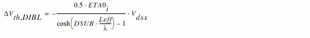
Drain Induced Barrier Lowering (DIBL)
Vt Roll on/off at moderate channel lengths
Vt Roll on/off at moderate channel lengths and high Vds

Body Doping Effects
Body Doping Effect

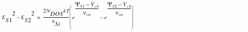
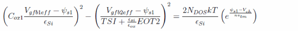
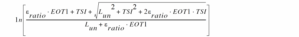
Surface Potential Calculation
Surface Potential is computed solving the Poisson's equation in silicon body:


The first equation above is simplified, replacing vtm by nvtm and neglecting the second exponential term on right side. Further approximating ![]() s2 to be
s2 to be

The simplified Poisson’s equation obtained is:

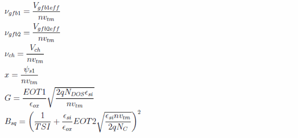
Solving the above equation using an iterative Halley’s algorithm for a maximum of four iterations stopping when the error in surface potential solution is below 1 nV. Halley's algorithm is a second order Householder's method and can be written as:

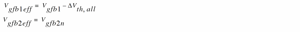
Simplifying the first equation assuming the back-gate to remain always in weak inversion, reducing it to become a function of only the front-gate parameters:
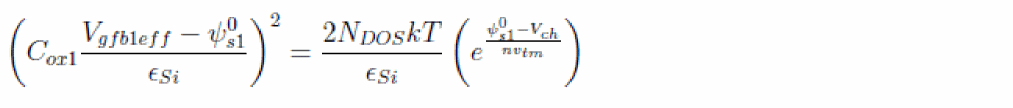
The above equation is solved using two iterations of Halley's algorithm and can be written as:
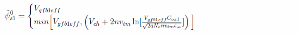
Once x satisfying is known, ![]() s1 is obtained from
s1 is obtained from x using:
The equation is solved once at the source side, with Vch = 0, and once at drain side, with Vch = Vds, to obtain the surface potentials at the two ends of the channel.
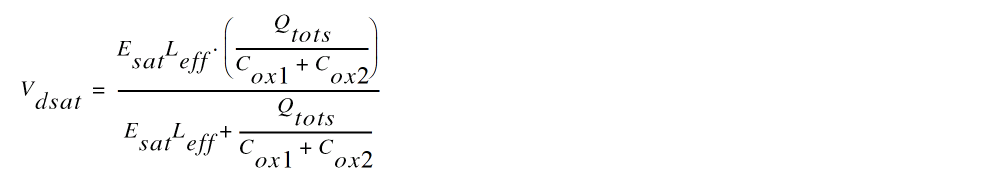
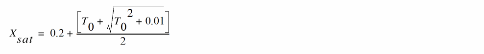
Drain Saturation Voltage
The drain saturation voltage model is calculated after the source-side surface po-tential (![]() s) has been calculated. Vdseff is subsequently used to compute the drain-sidesurface potential (
s) has been calculated. Vdseff is subsequently used to compute the drain-sidesurface potential (![]() d).
d).
Electric Field Calculations


Calculate the Drain Saturation Voltage

If Drs is not equal to 0, then


Calculate Average Field, Potential, and Charge
Average Field, Potential, and Charge


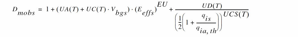
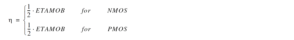
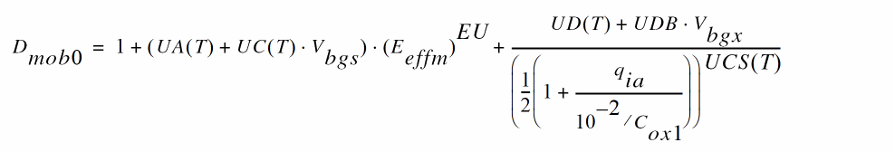
Mobility Degradation
The mobility model is based on the BSIM4 model.


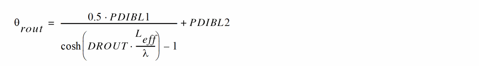
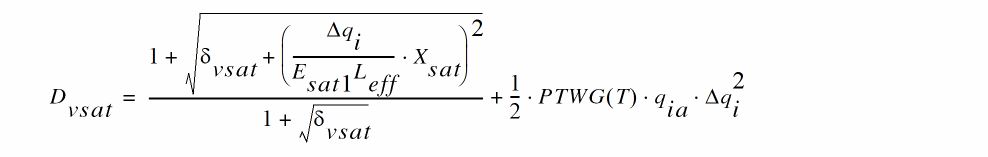
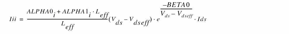
Output Conductance
Channel Length Modulation


Output Conductance due to DIBL


Moc is multiplied to Ids in the _nal drain current expression.
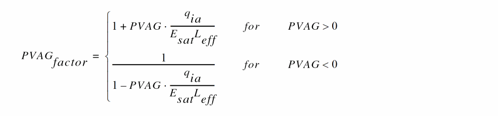
Veolocity Saturation
Current Degradation Due to Velocity Saturation
The following formulation models the current degradation factor due to velocity saturation in the linear region. It is adopted from the BSIM5 model.

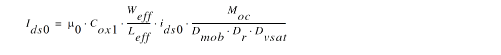
Drain Current Model
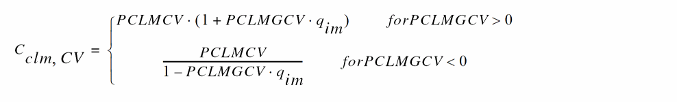
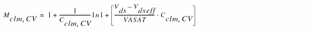
C-V Model
Channel Length Modulation
Assign Variables


Parasitic Resistance and Capacitance Models
BSIM-IMG models the parasitic source/drain resistance in two components, a bias dependent extension resistance, and a bias independent diffusion resistance.
The parasitic capacitance model in BSIM-MG includes a bias-independent outer fringe capacitance, a bias-dependent inner fringe capacitance, a bias-dependent overlap capacitance, and substrate capacitances.
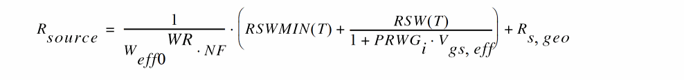
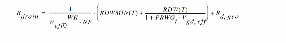
Bias-dependent Extension Resistance
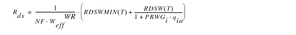
RDSMOD=2 (Internal and Geometry dependent)
Bias-independent Diffusion Resistance
Overlap Capacitance Model
Outer Fringe Capacitances
Inner Fringe Capacitance


Source/drain to Substrate Capacitances
Impact Ionization and GIDL/GISL Model
Impact Ionization Current
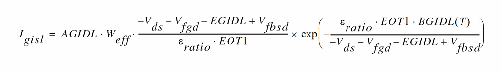
Gate-Induced-Drain/Source-Leakage Current

Gate Tunneling Current
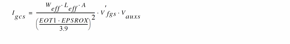
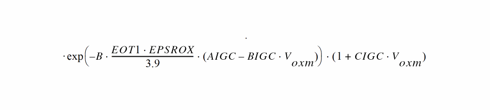
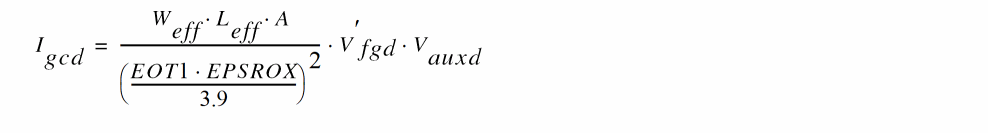

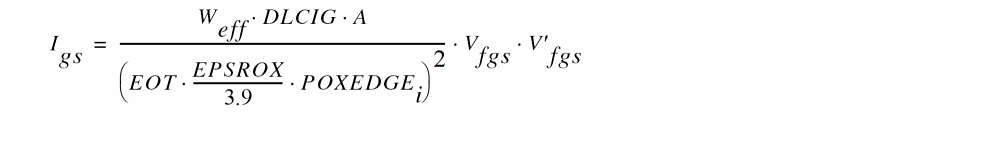
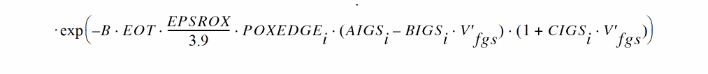
Gate to source/drain current (Igs, Igd)

Self Heating Model
Figure -1 R-C network for self-heating calculation
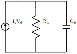
Thermal resistance and capacitance calculations

Noise Modeling
Following noise models are available in BSIMIMG 102.6.1:
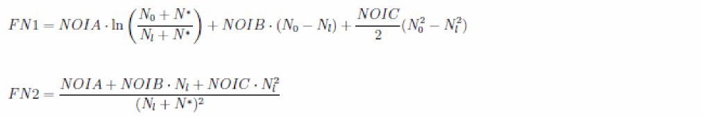
Flicker Noise Model
In BSIMIMG102.6.1, the flicker noise model is same as FNOIMOD=1 in BSIM4. The unified physical ficker noise model is smooth over all bias regions. The physical mechanism for the ficker noise is trapping/detrapping-related charge fluctuation in oxide traps, which results in fluctuations of both mobile carrier numbers and mobilities in the channel. The unified flicker noise model captures this physical process. In the inversion region, the noise density is expressed as:
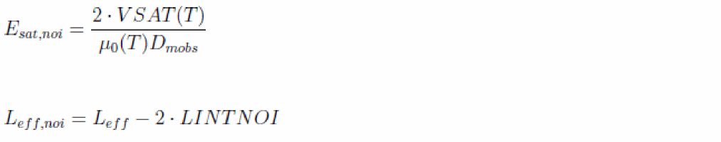
The channel length reduction due to channel length modulation and given by:

Charge density at the source side is given by:

Charge density at the drain side is given by:


where CIT is a model parameter from DC IV.
In the strong inversion region, the noise density is written as:

In the subthresold region, the noise density is given as:

The total flicker noise density is given by:

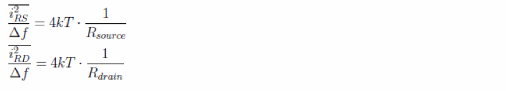
Thermal Noise Model
For TNOIMOD=0 (Charge-based model), the noise current is given by:
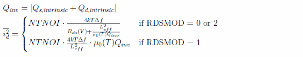
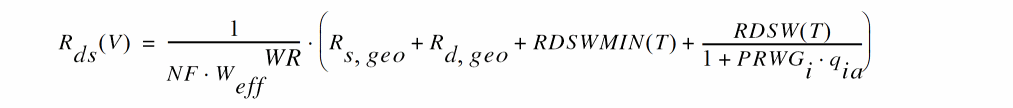
where Rds(V ) is the bias-dependent LDD source/drain resistance, and the parameter NTNOI is introduced for more accurate fitting of short-channel devices. Qinv is the total inversion charge in the channel. Qs,intrinsic, Qd,intrinsic are intrinsic charges at source/drain ends.
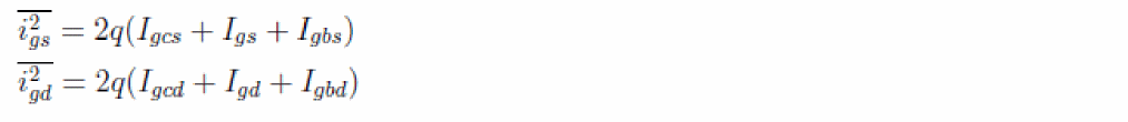
Gate Current Shot Noise
Resistor Noise Model

Return to top