3
Example: Design Entity
A design entity represents a portion of a hardware design that performs a well-defined function and has well-defined inputs and outputs. A design entity can represent an entire system, a subsystem, a board, a chip, a macro-cell, a logic gate, or any level of abstraction in between. A design entity is defined by an entity declaration together with a corresponding architecture body.
Design entities can be described by using a hierarchy of blocks where each block represents a portion of the whole design. The design entity itself is the top-level block, known as an external block, that resides in a library and can be used as a component of other designs. Internal blocks are nested in the hierarchy and defined by block statements.
A design entity can also be described in terms of interconnected components. Each component can be bound to a lower-level design entity to define the structure or behavior of that component. Successive decomposition of a design entity into components, and binding those components to other design entities that can be decomposed in the same manner, results in a hierarchy of design entities representing a complete design. A collection of design entities is a design hierarchy. The bindings necessary to identify a design hierarchy are specified in a configuration of the top-level entity in the hierarchy. A configuration is defined by a configuration declaration. A configuration is used to describe how design entities are put together to form a complete design.
Illustrated Example of an Inverter Model
This example is a mixed-signal model of an inverter. The input is a bit signal that is converted to a 5V or 0V. This value is then given to the input of the cmos inverter and the output of the cmos inverter is then given to an analog to digital converter. The final output is a bit signal that is the inverse of the input bit signal.
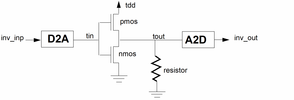
This inverter can be modeled with the following entity and architecture.
entity inverter is
    port(inv_inp : in  bit;
      inv_op  : out bit);
end entity inverter;
architecture inv_behav of inverter is
    terminal tin, tout, tdd : electrical;
    quantity vdd across idd through tdd;
    quantity vin across iin through tin;
    quantity vout across tout;
    quantity vres across ires through tout;
    signal vsig : real := 0.0;
    constant power : real := 5.0;
    constant r : real := 1.0;
    component nmos is
     port (terminal g, s, d : electrical);
 end component;
 for all : nmos use entity work.nmos(nmos_behav);
 component pmos is
  port (terminal g, s, d : electrical);
 end component;
 for all : pmos use entity work.pmos(pmos_behav);
begin
    vres == r * ires;
    vdd == power;
    vin == vsig’slew(1.0,-2.0);
    break on vsig;
    nm : nmos port map(tin, ELECTRICAL_REF, tout);
    pm : pmos port map(tin, tdd, tout);
    d2a: process(inv_inp)
    begin
     if (inv_inp = '0') then
   vsig <= 0.0;
  else
   vsig <= power;
  end if;
 end process;
 a2d : process (vout’above(power/2.0))
 begin
  if(vout’above(power/2.0) = true) then
 inv_op <= ’1’;
 else
   inv_op <= ’0’;
 end if;
 end process;
end architecture inv_behav;  ---- of inverter
The interfaces for the nmos and pmos components are declared in the architecture description inv_behav. In this case the architecture is written in the dataflow style because the design uses signal ports with direction. The syntax for declaring and instantiating components are covered in more detail in Component.
The resistor is modeled with a simple simultaneous statement. (For more information, see “Simultaneous Statements”.)
vres == r * ires;
The d2a and the a2d are modeled as processes. The d2a process assigns the vsig signal a value of 0.0 if the input is 0, otherwise it assigns a value of 5.0 (power). The following simple simultaneous statement specifies that the vin across quantity follows the value of vsig but with a rising slope of 1 and a falling slope of -2.:
vin == vsig'slew(1.0,-2.0);
The vdd across quantity has a constant value of 5.0 (power):
vdd == power;
The tin terminal is connected to the gate port and the tout terminal is connected to the drain ports on the nmos and pmos instances. The nmos source port is tied to ground (the reference terminal) and the pmos source port is tied to the tdd terminal:
nm : nmos port map(tin, ELECTRICAL_REF, tout);
pm : pmos port map(tin, tdd, tout);
The a2d process converts the analog value back to digital. If the value of vout is greater than 2.5 (power/2) then inv_op is assigned a value of 1. Otherwise inv_op is assigned a value of 0. The expression vout’ABOVE(power/2.0) tests whether vout is greater than 2.5.
Return to top