1
Introduction to Virtuoso RF Solution
The Virtuoso Multi-Technology Solution has enabled designers to create packages in Virtuoso by adding package design capabilities to the existing capabilities of Virtuoso. With the Virtuoso RF Solution, the Virtuoso Multi-Technology Solution is leveraged for RF module designers who want to edit, simulate, extract, and backannotate in Virtuoso. The rapid increase in design complexity and heterogeneous integration is driving the need to do simultaneous design in the package and die. This simultaneous, but often disjointed, development flows of the package and die increase the chance of design failure. The Virtuoso Multi-Technology Solution has been developed to allow the package and die designs to evolve simultaneously and Edit-in-Concert with one another within Virtuoso. Layout versus Schematic (LVS) integrity can be maintained during logic and placement changes in the package and die. In addition, the Virtuoso RF Solution gives package layout designers productivity-enhancing features to run a variety of EM solvers integrated into Virtuoso. Designers can fine-tune portions of the system by extracting and simulating circuit paths and context around the circuit paths.
In low frequency and less demanding environments, IC (Die) designs are relatively unaffected by the package context in which they were used. The IC (or die) in-package behavior is typically in line with standalone simulation results. Packages are now expanding from a single IC to multiple ICs with interconnects and discrete components required by the ICs to function. The PCB may contain several packages with associated interconnects and more discrete components. When the IC behavior is measured, housed inside a package and mounted on a PCB, there is a visible deviation compared to the standalone simulated characteristics of the IC. This deviation is more pronounced at higher frequencies and/or more demanding EM environments. To identify and eliminate such errors at an early design stage and prior to tape-out, it is essential to have a familiar design and simulation environment, which auto-enables the IC or package designer to simulate the IC in context of the entire PCB, package system, and the parasitics. The methodology just described has a two-fold impact: it allows an optimization of the design of the package and PCB in the context of IC, and in certain cases might require redesigning the IC itself. The entire control lies with the IC or package designer, who is in a much better position to minimize design iterations.
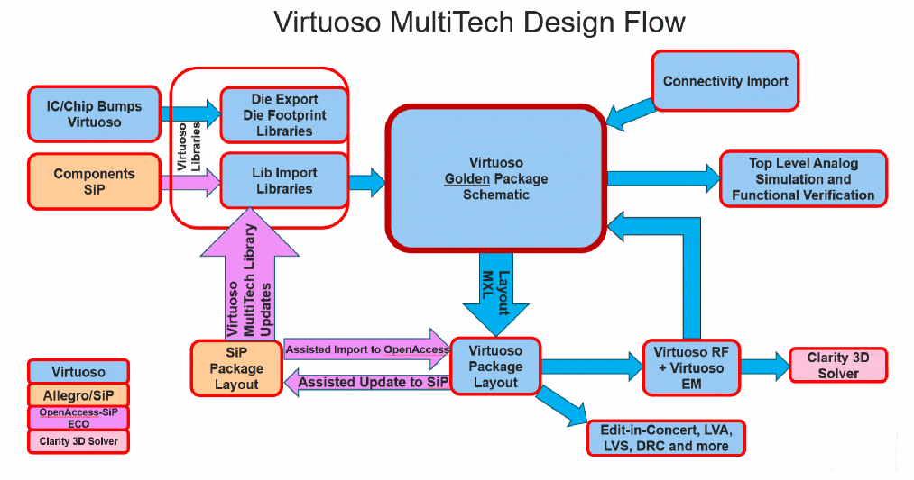
The Virtuoso RF Solution in the Virtuoso environment allows ICs to be imported from different technologies and assembled in a package schematic. At times, the IC and package designer work in isolation and make changes to the schematic. The LVS checks, simulations, and EM simulations play an important role in synchronizing and consolidating the changes in the package layout. Flows in the Virtuoso RF Solution enable the package designers to assemble and simulate the package on one platform.
Related Topics
License Requirements of Virtuoso RF Solution
Schematic/Layout Views in the Virtuoso RF Solution/Virtuoso MultiTech Environment
Return to top