|
Package Terminology
|
Definitions
|
|
Package
|
A physical symbol designated as the Drawing Type package in the Symbol Editor. Typically used as the database element for components that have electrical connectivity. Stored as a library element with an extension of .psm. A package contains the padstacks, labels, outline, TILPs, and so on. It visually represents the component in Layout MXL. Note that a single package may consist of a symbol or multiple logical symbols.
|
|
SMD (Surface Mounted Device)
|
A technology using surface-mounted components that have pins glued to the surface of a design. Designs that contain SMDs can have components at the top and bottom.
|
|
Embedded Component
|
Embedded technology plays an active role in shrinking interconnect path between components and reducing the transmission loss. Embedded components could be Active Devices (ADs) or Passive Devices (PDs). Embedding components leads to reduction of connection points, external pads, number of through holes, and lead length so that circuit board integrity can be improved and parasitic inductance of printed circuit can be decreased.
|
|
Transmission Line
|
An electric conductor exhibiting series inductance and shunt capacitance distributed along its length and logically divided into chunks. A signal must charge up each chunk or inductance and capacitance before it is passed along to the next chunk, therefore, reducing the propagation velocity.
|
|
Heterogeneous Integration
|
Heterogeneous integration is about integrating components with different functionalities and thicknesses, or could be available in the market as pre-packaged components with solder terminations, such as BGA, CSP, in the inner layer of PCBs as assembled components. Using packaging technology to integrate dissimilar chips with different functions instead of integrating all the functions into a single chip and going for finer feature size achieves this.
|
|
Die, Die pad, Die Stack
|
Die is an unpackaged chip.
Die pad is a metal contact on the die of an IC that is used to make electrical connections between the IC and the component (also called I/O pad or die pin. For flip-chip, they are called solder bumps, while for wire bound ICs they may be called bond wire pads). In IC tool terminology, wire bonded ICs are often referred to as bond pads.
Die stack is a vertical stack of dies consisting of one or more dies, spacers, and interposers.
|
|
Bond wire, Bond finger
|
A wire (usually gold) that connects a die pad to its respective bond finger on the component substrate or to another die pad on another die.
A metal pad on the outer layer of component substrate to which a bond wire will be attached to form an electrical connection between the component and die.
|
|
Flip Chip
|
An unpackaged integrated circuit that connects to a hybrid circuit by means of solder bumps on its faces that correspond to its pin-outs.
|
|
Silicon Substrate
|
The silicon "wafer" onto and into which the IC circuitry is placed.
|
|
BGA, LGA
|
Ball grid array (BGA) is a type of die component whose pins are solder balls arranged in a grid pattern.
Land grid array (LGA) is a a type of die component with a rectangular grid of solder balls on the underside of a package.
|
|
Interposers
|
A substrate with a single conductor layer that is used in the manufacture of a die stack to support the die connectivity. It provides the capability to wire bound dies whose die pad positions create the wire-bound lateral spans that are beyond the physical limits of a wire-bounding machine.
|
|
Vias
|
An opening in a dielectric layer that connects adjacent conductor layers. A via is a plated-through hole with ETCH/CONDUCTOR on every ETCH/CONDUCTOR subclass. Vias make it possible to route a single connection through more than one ETCH/CONDUCTOR subclass. Also called a feedthrough.
|
|
Padstack
|
A list of all data for each pad definition in the design drawing; each pin and via refers to a padstack for size, shape, and drill information.
|
|
Cut Shapes, Drill Holes
|
Cut shapes is about trimming the conductive planes in the PCB into separate electrical pieces.
Drill holes are important for multilayer PCB. These holes are used for electrical connection between each layers and fix or position the components.
|
|
Technology Independence
|
The ability to be used in any design and accept user-preferred units, constraint and parameter values, and user properties on any platform.
|
|
TILP
|
Technology Independent Layout Pcells (TILPs) are created from the die symbols, which have been created from exporting the die. TILPs are added to the libraries from importing into the package layout.
|
|
Planes
|
A conductive layer in the cross-section editor designated as layer type "plane". These layers are typically used to create shapes for the purpose of Power and GND distribution. These layers exist within the component substrate that routes the signals and distributes the power from the die to the host PCB.
|
|
Voiding Shape
|
A void is generated for dynamic shapes when a change is made that affects the shape connectivity. It insulates the signal shapes from other shapes, such as power and ground. Voiding associated with the rectangular pads maintains a more consistent minimum clearance to the pad boundary. It improves the copper shape flow between the adjacent rectangular pads.
|
|
IC and Package Shape Interface
|
IC and package interconnect, which is through bond wires or IO pads.
|
|
Significance of Ground and Power Planes in Packages
|
Ground and power plane is also a shape in package. The package traces are long and they behave like transmission lines. Therefore, there is a need to provide a return path for it. On the other hand, IC traces are short so no planes are needed for return path. Power planes reduce the impedance of the power net which, in turn, reduces the voltage drop.
|
|
Stackup
|
The arrangement of copper layers and insulating layers that make up a PCB prior to the board layout design. While a layer stack-up allows you to get more circuitry on a single board through the various PCB board layers, the structure of PCB stack-up design has many other advantages:
-
Minimize the circuit's vulnerability to external noise as well as minimize radiation, reduce impedance, and crosstalk concerns on high-speed PCB layouts.
-
Balance the need for low-cost, efficient manufacturing methods with concerns about signal integrity issues
-
Enhance the electromagnetic compatibility of the design as well.
|
|
WLP
|
Wafer-level packaging (WLP) is the technology of packaging an IC that is the part of the wafer itself. It involves attaching the top and bottom outer layers of packaging and the solder bumps to ICs on the wafer, and then dicing the wafer. All packaging and interconnection must be fabricated on the wafer prior to dicing.
|
|
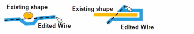
Hug
|
A mode in which the edited wire avoids moving the existing shapes and respects minSpacing value set between the wire and the existing shapes.
|
|
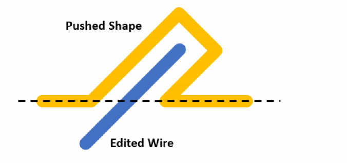
Shove
|
A mode in which an edited wire pushes the non-static shapes when it is extending and respects minSpacing values set between the wire and the existing shapes.
|