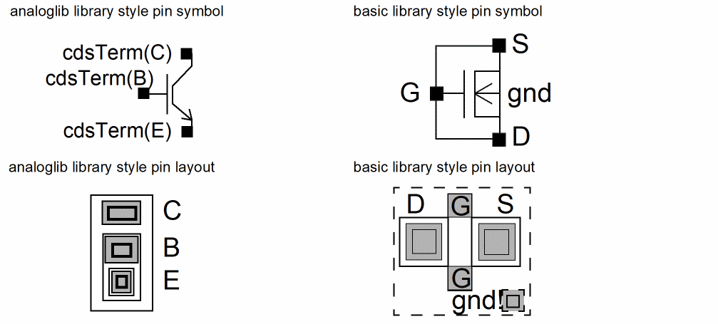
Pins and Pin Names in Layout XL
For connectivity assignment tracing and cross-probing to work correctly in Layout XL, the pins and pin names in the layout cellview of a device must match those in the corresponding schematic symbol.
Extra Pins in the Symbol or Layout Views
Layout XL cannot maintain connectivity for any extra pins in the symbol view because there is no corresponding pin for the device in the layout view.
Conversely, Layout XL maintains connectivity for extra pins whose names are global nets (for example, vdd!) in the layout view. It also maintains connectivity for any extra pins in the layout that have their connectivity defined by inherited connections. The inherited connection can be defined relative to the layout instance itself or relative to the schematic hierarchy that ends with the schematic instance corresponding to that layout instance.
The look-up order used by Layout XL to determine the net to connect to an extra pin is:
- Inherited net expression on the layout pin.
-
Global net — global attribute or
!at the end of the net name. -
Property named
sub,sub_inh, orbnon the layout master.
Related Topics
External Connections
You can also define pins to be connected externally to the design.
The commands in the Connectivity – Pins submenu let you connect pins in four different ways.
- Must Connect connects selected pins in a net externally at a higher level of the hierarchy.
- Strongly Connected connects selected pins within the device. By default, pins are connected internally (strongly).
- Weakly Connected connects selected pins in a limited external connection to avoid specific internal connections (typically ones with high-resistance paths).
- Pseudo Parallel Connect connects selected instance terminals on the same net within an instance as though they were connected externally; that is, they are defined as a connection but need never be physically connected.
Related Topics
Return to top