Metal-Insulator-Metal Capacitor (MIMCAP) Stack
A Metal-Insulator-Metal Capacitor (MIMCAP) stack uses a cut layer that connects a metal layer of a higher mask number, such as M(n+1), to another metal layer of a lower mask number, such as M(n), and to two intermediate layers.
The intermediate layers in such a connectivity stack are used to define capacitors and these layers are defined in the technology file with the mimcap function.
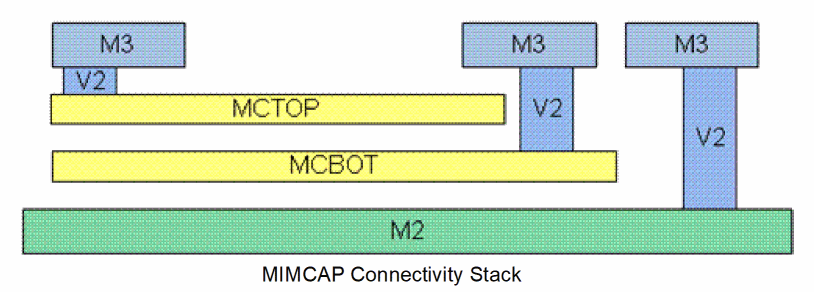
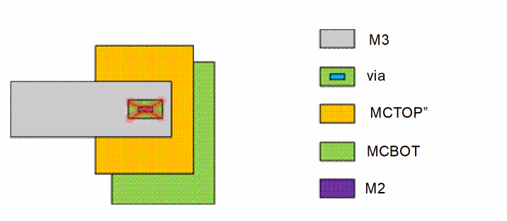
The figure below represents a MIMCAP connectivity stack. Here, the cut layer, V2, connects the metal layer, M3, to another metal layer, M2, which has a lower mask number. In addition, the cut layer connects the top metal layer to intermediate metal layers, MCTOP and MCBOT.
In the technology file, the connectivity stack represented above is defined with the viaDefs:
"M3_M2": M3 -> V2 - > M2
"M3_MCTOP": M3 - > V2 - > MCTOP
"M3_MCBOT": M3 - > V2 - > MCBOT
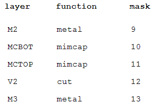
The corresponding layer function table can be represented as:
Alternatively, the cut in a MIMCAP stack may not stop at another MIMCAP layer but can go all the way down to the bottom metal layer. This means that all the layers between the top and bottom metal layers are connected by the cut shape, as shown in the figure.
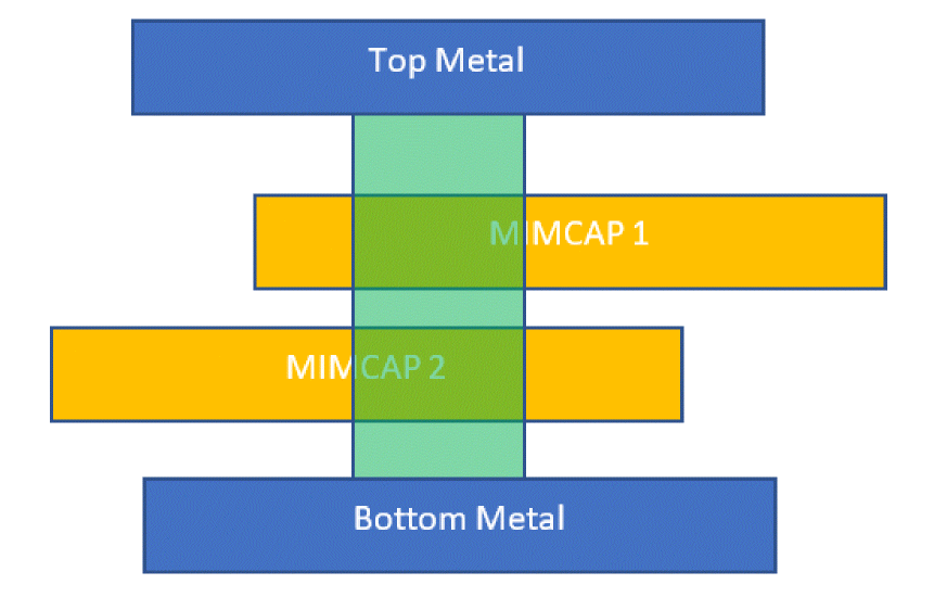
For the connections in such a stacked MIMCAP to be correct, all the viaDefs must be present in the validVias constraint of the extractor constraint group. For example, for the connections in the given stacked MIMCAP figure to be correct, the following viaDefs should be present in the validVias example: Top/MIMCAP1, Top/MIMCAP2, Top/Bottom, MIMCAP1/MIMCAP2, MIMCAP1/Bottom, MMCAP2/Bottom.
In the technology file, the viaDefs definition of the stacked MIMCAP is:
"Top_Mimcap1": Top -> V -> Mimcap1
"Top_Mimcap2": Top -> V -> Mimcap2
"Top_Bottom": Top -> V -> Bottom
"Mimcap1_Mimcap2": Mimcap1 -> V -> Mimcap2
"Mimcap1_Bottom": Mimcap1 -> V -> Bottom
"Mimcap2_Bottom": Mimcap2 -> V -> Bottom
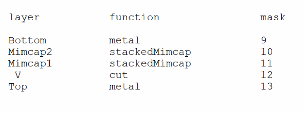
The corresponding layer function table can be represented as:
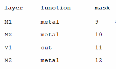
Two-Metal Stack
A “two-metal” stack uses a cut layer that connects a metal layer of a higher mask number, such as M(n+1), to another metal layer of lower mask number, such as M(n), and to a single intermediate metal layer.
The figure below represents a “two-metal” connectivity stack. Here, the cut layer, V1, connects the metal layer with a higher mask number, M2, to another metal layer, M1, which has a lower mask number. In addition, the cut layer connects the top metal layer to an intermediate metal layer, MX.
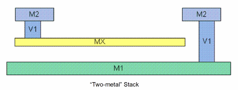
In the technology file, the connectivity stack represented above is defined with the viaDefs:
“M2_M1”: M2 - > V1 - > M1
“M2_MX”: M2 - > V1 - > MX
The corresponding layer function table can be represented as:
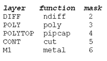
Poly-Insulator-Poly Capacitor (PIPCAP) Stack
A Poly-Insulator-Poly Capacitor (PIPCAP) stack uses a cut layer that connects a metal layer to two poly layers. The poly layer at the bottom is routable, whereas the poly at the top is nonroutable and is used to define capacitors. The technology file defines the top poly layer by using the function, pipcap.
The figure below represents a PIPCAP connectivity stack. Here, the cut layer, CONT, connects the metal layer, M1, to two poly layers, POLYTOP and POLY.
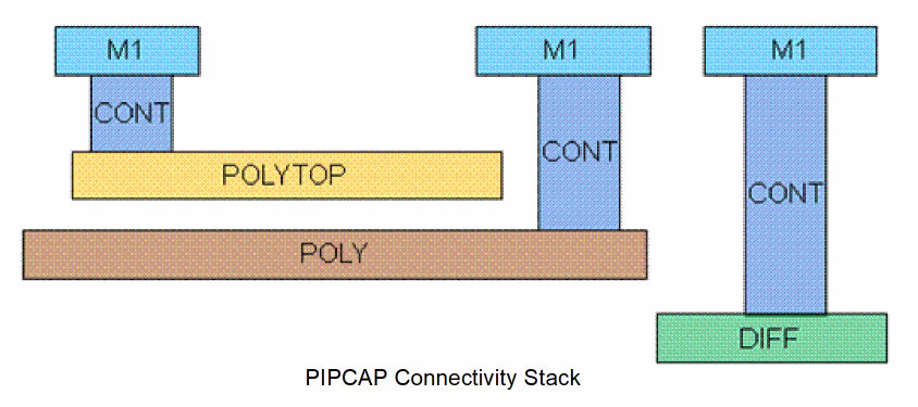
As displayed in the figure, the cut layer can also connect the metal layer, M1, to the diffusion layer, DIFF. To ensure that the top poly layer does not overlap diffusion, the top poly layer must be enclosed within the bottom poly.
In the technology file, the connectivity stack represented above is defined with the viaDefs:
“M1_DIFF” : M1 - > CONT - > DIFF
“M1_POLYTOP”: M1 - > CONT - > POLYTOP
“M1_POLY” : M1 - > CONT - > POLY
The corresponding layer function table can be represented as:
Illegal Via Connections
The extractor checks that the top and bottom layers of a via are effectively connected. If a violation is identified, the extractor creates an "Illegal via connection" marker on the via.
Let us consider a MIMCAP parallel connectivity stack as displayed in the figure below. Here, the metal layer M3 is connected to metal layers, MCTOP, MCBOT, and M2 through the same cut layer, V2.
The viaDefs for the parallel connectivity stack are defined in the technology file as:
“M3_M2” : M3 -> V2 - > M2
“M3_MCTOP”: M3 - > V2 - > MCTOP
“M3_MCBOT”: M3 - > V2 - > MCBOT
In the figure, the via is expected to connect the shape on M3 to a shape on MCBOT. But, a shape on MCTOP overlaps the via, preventing the connection. However, due to the overlap with the shape on MCTOP, the via effectively connects the shape on M3 to the shape on MCTOP. As this was not the expected connection, the extractor creates an “illegal via connection” marker on the via.
Related Topics
Return to top