Pin Placement Form
Use the Pin Placement form to place and optimize pins your design.
This form consists of two tabs:
Pin Planner tab
The following table describes the fields available on the Pin Planner tab of the Pin Placement form.
| Field | Description |
|---|---|
|
This section lets you specify the scope for running the Pin Planner. |
|
|
Applies the form settings only to the top-level pins in the design. |
|
|
Applies the form settings to pins of the selected soft block in the design. Select the required soft block from the drop-down list. If you have already selected a block in the canvas, that block is automatically selected in the Pin Planner tab. If you have more than one block selected in the canvas, the first block you selected is the one selected in the form. |
|
|
Zooms to the selected soft block automatically and switches to Level-1 Pins mode when you click a soft block in the design canvas. This option is off by default, which means that when you click a soft block, the soft block is selected, but you remain at the top level. |
|
|
This section filters the pins listed in the form. Use a combination of the two pull-downs to filter the pins that are displayed. Alternatively, you can use the By Name field to filter the pins by name. |
|
|
Filters pins based on the edge to which they are assigned. The available edge options are All, Left, Top, Right, Bottom, Level-1 pin, Top-Level Route, To Hard Block Multi Pin, and Hard Block Multi Pin. |
|
|
Filters pins based on their placement status or pin types. The available options are All, Placed, Unplaced, Locked, Fixed, Ordered, Unordered, I, O, and IO. |
|
|
Filters pins based on their names. The default regular expression for this filter is “.*” (dot asterisk), which implies that a name filter is not applied. Therefore, all the pins in the design are displayed. Other supported regular expressions are:
|
|
|
Lists all the shape pins found in the current scope. It does not list pins that are vias. The entries are expressed as termName:pinName:figName because the pin figure is the physical entity that you are placing. If a pin has more than two pin figures attached to it, but the pin figures have the same name, they are represented by a single entry in the pin table. The other columns in the pin table are the Edge to which the pin is assigned, the Order in which the pins are placed, and the Status, Type, Layer, Width, Height, and Connectivity of the pins. You can sort the table by any column by clicking the relevant column header. Click again to reverse the sort order. The Connectivity column annotates whether pins are connected to buried pins or multiple hard block pins. |
|
|
This section specifies the pin attributes of the pins in the pin table. |
|
|
Specifies the edge on which the selected pins are to be placed. The options are Left, Top, Right, Bottom, Level-1 pin, Top-Level Route, To Buried Pin, Level-1 Route, To Hard Block Multi Pin, Any, and As is. The As is setting allows the edge settings of pins to remain intact when changing the Order or Placement Status Constraint properties. Depending on the block type, the pin edges are snapped to either the manufacturing grid or the routing grid. If the block type is custom, the pin edges are snapped to the manufacturing grid. If the block type is digital, the pin edges are snapped to the routing grid. |
|
|
Specifies the order in which the selected pins are to be placed. You can specify an order only if you have assigned the pins to an edge. To place the pins unordered, leave the field blank or type “-”. To specify an order for the pins, enter a value. |
|
|
Specifies the status to be assigned to the pins after they are placed.
|
|
|
Specifies the layer on which the pin shapes are to be drawn. Layer purpose names are filtered dynamically as you type a value in the Layer field. By default, the width, height, and layer of the pin selected in the pin table is displayed. When you change the layer, Pin Planner checks whether the pin width and height values are valid. These values cannot be lesser than the layer |
|
|
Specifies which pins are to be updated with the new attributes when you click Apply.
|
|
|
This section lets you specify how the selected pins are to be spaced. Spacing values are enforced only between adjacent pins on an edge, even if the spacing is set between two non-adjacent pins. If you specify a spacing between a pin and an iterated pin, the software applies the spacing between the last pin of the iterated pin and the individual pin. If the specified spacing cannot be satisfied, you see a warning in the CIW and the pins are not moved. Pins are spaced and constraints are updated only by clicking one of the Space buttons in this section and not by clicking the Apply button in the Attributes section of the Placement Planning form. |
|
|
Specifies the distance by which the selected pins are to be spaced. |
|
|
Updates the constraints that are applicable to the design automatically (for example, alignment constraints on the selected pins) based on the settings in the Pin Spacing section. If a pin to be spaced has the alignment constraint set, the placer reads the constraint to determine the appropriate access direction for the pin. |
|
|
Spaces out reference pin from the leftmost pin on the top and bottom edges (0 in the example) and the bottom pin on the side edges (C). Environment variable: pinSpacingFrom 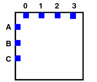 |
|
|
Spaces out the center pins on all edges as reference. On the left edge in the example above, this is pin B. On the top edge, the pin spacer divides the total number of pins by 2 and uses the result as the reference pin (2). |
|
|
Spaces out the rightmost pin on the top and bottom edges (3) and the top pin on the side edges (A). |
|
|
Interleaves bits of the selected iterated pins by applying an order constraint that specifies how the individual bits are to be placed. |
|
|
Reverses the interleaving of the selected iterated pin bits. |
|
|
Performs the Expand or Collapse function on all the pins in the list box. |
|
|
Performs the Expand or Collapse function only on the selected pins. |
|
|
Elongates the selected pins vertically from the top edge of the boundary to the bottom. |
|
|
Elongates the selected pins horizontally from the left edge of the boundary to the right. |
|
|
This section lets you zoom the display to the currently-selected pins. |
|
|
Enables the zoom functionality. Drag the slider active to set the desired zoom level. The acceptable zoom range is between
Alternatively, set the environment variable
If you set the auto zoom level to a value less than 0 when using the |
Pin Optimization tab
The following table describes the fields available on the Pin Optimization tab of the Pin Placement form.
| Field | Description |
|---|---|
|
Specifies the pins to be optimized.
Environment variables: pinOptMode, selectedOnly |
|
|
This section specifies the minimum spacing between the pins. |
|
|
Scales up the spacing values as per the table spacing rules defined for different widths of the pins. If this option is turned off, then use the minimum spacing values that are defined for the layers in the technology file. Environment Variable: tableSpacingRule |
|
|
Indicates that the minimum spacing values are to be based on the line-line spacing mode. If the Use Table Spacing check box is selected, then the spacing values are defined as per the table spacing rules for different pin widths. Environment Variable: spacingMode |
|
|
Enables the Options and Advanced Options buttons. Environment variable: customPinGrid |
|
|
Displays the Pin Spacing Options form, which lets you specify the pin spacing values for each layer. |
|
|
This section specifies the distance between the adjacent side and the center point of the first pin. Pin offset defines the first valid point for placing a pin on a grid. Pin offset values are layer aware, which means that each layer can have a different pin offset value. |
|
|
Places the first pin on a grid such that it is aligned to the corner pins of the adjacent side and that there is no spacing violation. This is the default mode. Pin Optimizer also ensures that there is no wastage of grid space. In this mode, Pin Optimizer respects both, the pin spacing value and the pin pitch from the instance corners. |
|
|
Provides options to control the pin offset values for all layers in a design. Custom offset number is the value from the boundary edge to the first pin slot to which the pin needs to be centered. In this mode, Pin Optimizer respects the pin pitch values from instance corners, independent of offset mode. However, Pin Optimizer does not respect the pin spacing from instance corners, but ensures that pins do not lie outside the instance boundaries. When you select Custom, Options is made available.
Adding a pin grid adjustment factor for custom pins may be error-prone as the distance from the boundary edge to pin edge may not be the value used to adjust the offset.
Environment variables: offSetByGrids, offSetBySpacing, offSetMode |
|
|
Displays the Pin Offset Options form, which provides options to specify the pin offset values for all layers in the design. |
|
|
Specifies the Side of the block or the top-level PR boundary on which pins are to be placed. The valid values are: Left, Right, Top, and Bottom. Environment variable: targetPinSide |
|
|
Specifies that a check box is available for each side on which pins can be placed. In the image below, each check box shows the definition of that side for rectangular and rectilinear blocks. For rectilinear blocks, the Target Pin Side setting specifies the access direction for pins. 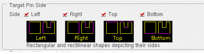 The Target Pin Side settings are considered after considering the constraints specified in the Constraint Manager. Pin Optimizer treats the edge of any soft block or top-level block as a range. Pin Optimizer places pins at different points of the range to find the best location so that minimum net length is achieved. |
|
|
Provides options to switch the pin layer depending on the side of the block on which the pin is placed by Pin Optimizer. See Setting Pin Layer and Side Constraints for Pin Optimization. Environment variables: enablePinLayerSideConstraints, bottomSidePinLayersConstraints, leftSidePinLayersConstraints, rightSidePinLayersConstraints, topSidePinLayersConstraints |
|
|
The options in this section are applicable only to nets with fixed (non-movable) pins connected to movable pins.
When Mode is set to All, pins on both side of nets are selected for optimization. Therefore, there are no reference (fixed) pins, and so the Match Fixed Pins Layer/Size settings are not applicable. To honor these settings, you must manually change the placement status of the required pins to fixed or locked. |
|
|
Provides options to change the layer and purpose of the 'to be placed' pins to match the layer and purpose of the connected fixed pins. For example, if a movable pin is on |
|
|
Changes the size of the movable pins to that of the connected fixed pins, select the Match Pin Size check box. For example if the target pin size is 0.6 x 0.6 and the reference pin size is 1.0 x 1.0, then selecting this option will change the target pin size to 0.6 x 0.6. |
|
|
Specifies the pin edge to be abutted to the PR boundary. It is applicable only to rectangular pins.The valid values are: As Is, Short Edge, and Long Edge. 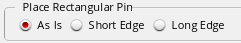 Environment variable: rectangularPinEdgeOnPRB |
|
|
Abuts the rectangular pin as-is to the PR boundary, irrespective of whether the abutted edge is short or long during pin optimization. Depending on the original position of the pin and the PR boundary side, either the long edge or the short edge of the pin is abutted to the PR boundary. 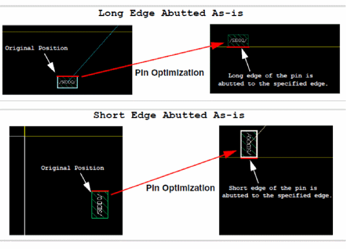 |
|
|
Abuts the short edge of the rectangular pin to the PR boundary during pin optimization. 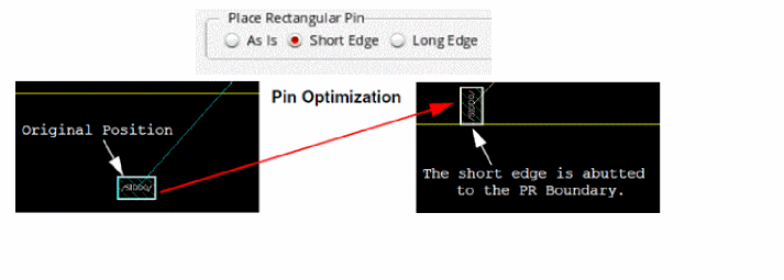 |
|
|
Abuts the long edge of the rectangular pin to the PR boundary during pin optimization. 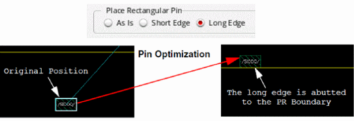 |
|
|
Snaps pins (selected or all) to their nearest WSP tracks by moving them by a minimum distance from their current position. The following constraints set on the pins are honored: Choose Honor Current Pin Location in the following situations:
When Honor Current Pin Location is selected, Pin Optimizer does not try to achieve the minimum net length.
Environment variable: honorCurrentPinLocation |
|
|
Runs Pin Optimizer in congestion-aware mode. See Congestion-Aware Pin Placement in Pin Optimizer. Environment variable: enableCongestion |
|
Related Topics
Planning Placement of Top-Level and Level-1 Pins
Return to top