1
Setting Up the Migration Example
CDS_AUTO_64BIT environment variable to ALL, unset the environment variable if you are using SpectreVerilog or UltraSimVerilog.Before the Spectre AMS Designer simulator, the major mixed-signal solutions on the market were SpectreVerilog and UltraSimVerilog. The AMS Designer simulator provides faster simulation speed, increased capacity, and enhanced features for handling more complicated mixed-signal designs with new technologies. More and more chip designers use Spectre AMS Designer for mixed-signal simulation and verification.
This migration example shows you how you would simulate a PLL design using UltraSimVerilog, SpectreVerilog, and, finally, AMS Designer using the same config view. You will learn about the OSS netlister, the ncverilog flow, using -v and -y command-line options, compiled Verilog-A, fastcross, and other AMS Designer features.
To set up the migration example, do the following in a terminal window:
-
Make and change to a directory for the migration example:
mkdir migrateToAMS
cd migrateToAMS
-
Copy the migration example files to this directory:
cp -r $CDSHOME/tools/dfII/samples/tutorials/AMS/MigrateFromCBNToOSSN.tar.gz .
-
Decompress the archive file:
gunzip MigrateFromCBNToOSSN.tar.gz
tar xf MigrateFromCBNToOSSN.tar
-
Change to the following directory:
cd MigrateFromCBNToOSSN
-
Source the setup file:
source SETUP
TheSETUPfile sets theTUT_DIRenvironment variable to your current directory:setenv TUT_DIR `pwd`
-
Start Cadence software:
virtuoso &
Features of the Migration Example
The migration example is a PLL design that has
- a 25 MHz input signal
- a 160 MHz output signal
- 305 MOSFETs
- 97 resistors
- 35 capacitors
- more than 30 behavioral modules
Testbench for the PLL Design
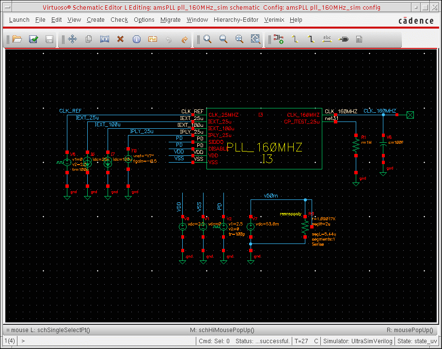
Here is the testbench schematic for the migration example (a PLL design).
Figure 1-1 Testbench Schematic for PLL Design
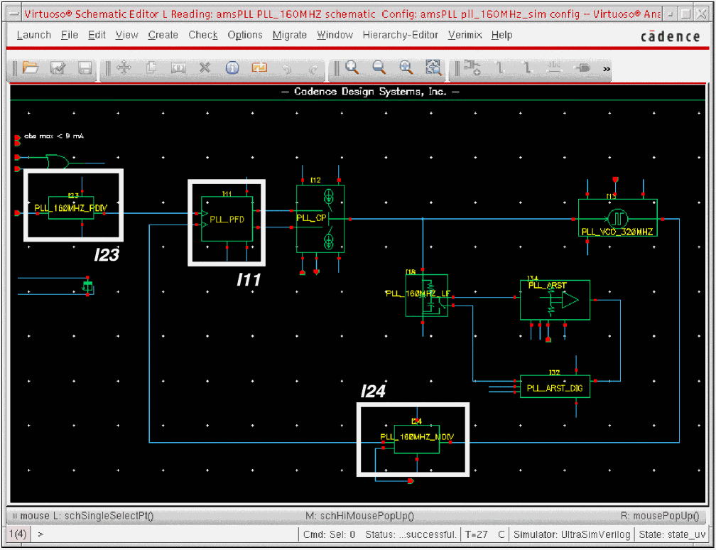
Inside the PLL_160MHZ Instance
Inside the I3 instance (PLL_160MHZ), the I23 instance (PLL_160MHZ_PDIV) outputs a 5 MHz reference signal for the loop. The I24 instance (PLL_160MHZ_MDIV) outputs a 160 MHz signal and a 5 MHz feedback signal for the PLL_FPD instance (I11).
Figure 1-2 Inside the I3 Instance
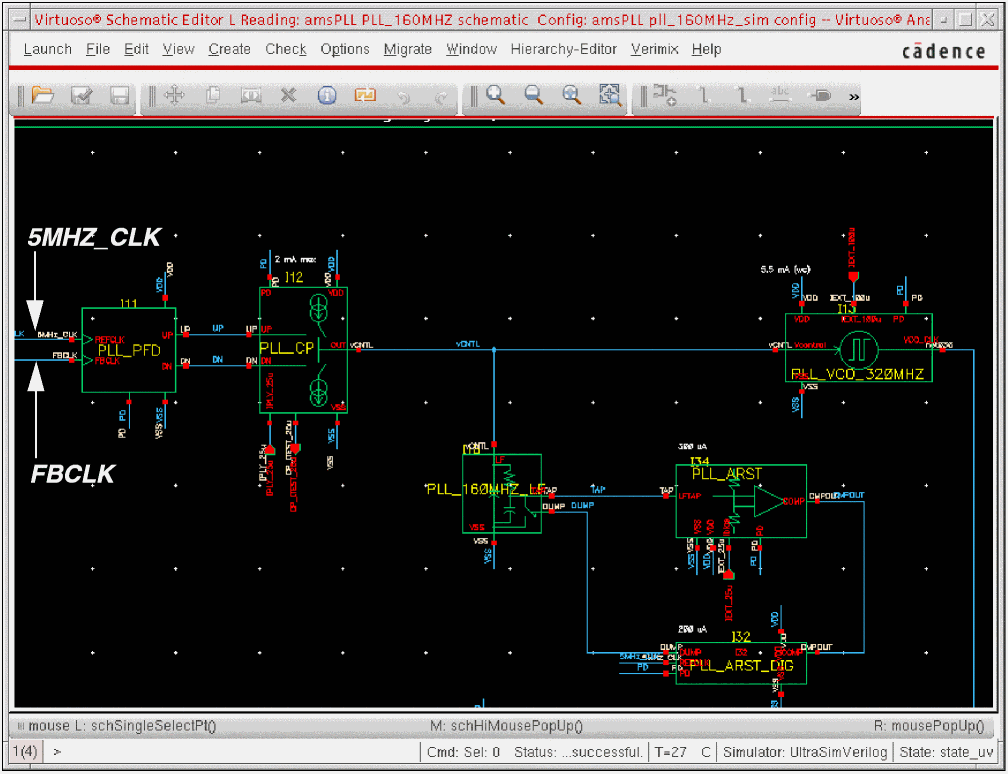
When the two PD input signals to I3 (see Figure 1-1) are out of sync, the PFD (PLL_PFD) generates corrective pulses (UP, DN) to adjust the charge pump output voltage (vCNTL) which controls the frequency of the VCO (PLL_VCO_320MHZ).
Figure 1-3 PFD Corrective Pulses, Charge Pump Output, VCO Input
Whenever the PLL is locked, the FBCLK and 5MHZ_CLK signals are in phase and the VCO control signal (vCNTL) is stable.
Return to top