3
Oscillators and Autonomous PSS Analysis
PSS analysis is capable of handling both autonomous (non-driven) and non-autonomous (driven) circuits. Autonomous circuits are time-invariant circuits that have time-varying responses. Thus, autonomous circuits generate non-constant waveforms even though they are not driven by a time-varying stimulus. Driven circuits require some time-varying stimulus to generate a time-varying response. The most common example of an autonomous circuit is an oscillator. Common driven circuits include amplifiers, filters, mixers, etc.
With driven circuits you specify the analysis period, which must be an integer multiple of the period of the drive signal or signals. Autonomous circuits have no drive signal and you do not know the actual period of oscillation precisely in advance. Instead, you specify an estimate of the oscillation period and PSS analysis computes the precise period along with the periodic solution waveforms.
When applied to autonomous circuits, PSS analysis requires you to specify a pair of nodes. In fact, this is how PSS analysis determines whether it is being applied to an autonomous or a driven circuit. If the pair of nodes is supplied, PSS assumes the circuit is autonomous; if not, the circuit is assumed to be driven. PSS analysis monitors the potential difference between these two nodes and uses it in the initial transient analysis portion of the autonomous PSS analysis; the signal is used to determine a better estimate of the period.
Phases of Autonomous PSS Analysis
A PSS analysis consists of two phases: an initial transient phase, which allows the circuit to be initialized, and the shooting phase, which is where the periodic steady-state solution is computed. The transient phase consists of three intervals. The first starts at tstart, which is normally 0, and continues through the onset of periodicity for the independent sources. The second is an optional stabilization interval, that you specify, whose length is tstab. The final interval of the transient phase is peculiar to the autonomous PSS analysis. In this phase, the length of which is four times the specified estimate of the oscillation period, the PSS analysis monitors the waveforms in the circuit and develops a better estimate of the oscillation period.
During the first stage of the transient phase, PSS extracts the fundamental frequency from the set of nodes specified in the PSS statement. During the second stage, the PSS analysis examines all the nets in your design to verify the accuracy of the extracted PSS fundamental frequency. This enhancement improves PSS analysis of circuits with frequency dividers by re-evaluating the PSS fundamental to take into account the frequency division in your circuit.
After the initial transient phase is complete, the shooting interval begins. In this phase, the circuit is repeatedly simulated over one period while adjusting the length of the period and the initial condition to find the periodic steady-state solution.
In some cases when an autonomous PSS analysis does not converge after a few iterations, increasing the tstab interval makes convergence faster and easier. Adjusting the tstab interval might improve the starting point for the shooting interval by moving it such that signals are quiescent or changing slowly. This allows strongly nonlinear circuits to converge faster.
For details of the algorithm for autonomous PSS analysis, see “Autonomous PSS Analysis”.
Starting the Oscillator
When applying PSS analysis to oscillators, you need to start the oscillator, just as you would if you were simulating the turn-on transient of the oscillator using transient analysis. The Designer’s Guide to Spice and Spectre [kundert95] describes in some depth techniques for starting oscillators.
In summary, there are two techniques for starting oscillators, using initial conditions, or using a brief impulsive stimulus. Initial conditions would be provided for the components of the oscillator’s resonator. If an impulsive stimulus is used, it should be applied so as to couple strongly into the oscillatory mode of the circuit, and poorly into any other long-lasting modes, such as those associated with bias circuitry.
Either way, after the trigger is applied to start the oscillator, it is important to allow the oscillator to run for a while before the shooting methods are applied to compute the steady-state result. To do so, specify an additional stabilization interval using the tstab parameter. In practice, an additional stabilization interval often improves convergence, especially when simulating high-Q oscillators.
Convergence Issues with Autonomous PSS Analysis
By their very nature, oscillators are quite nonlinear, which can cause convergence problems. If you experience convergence problems with autonomous PSS analysis, you should try one or more of the following suggestions.
- As with non-autonomous PSS analysis, providing a larger value for tstab generally improves convergence. While not always necessary, you occasionally need to set tstab to a value equal to or greater than the time needed for the circuit to approximately reach steady-state.
- Assure that whatever method you choose to start your oscillator is effective. It should “kick” the oscillator hard enough to start the oscillation and have it respond with a signal level that is between 25% and 100% of the expected final level. Avoid kicking the oscillator so hard that it responds in an unnecessarily nonlinear fashion. Also, try to avoid exciting response modes in the circuit that are unrelated to the oscillation, especially those associated with long time constants.
- Give a better estimate of the period. The simulator uses the estimate of the period you specify to determine how long the initial transient analysis interval is that is used to make a measurement of the oscillation period. If the period you specify is too short, it is not possible to get an accurate estimate of the oscillation period, and this might cause the PSS analysis to fail. Overestimation of the period is not a serious problem because the only penalty is a longer initial transient interval. However, significant overestimation might result in an excessively long simulation time.
-
While trapezoidal rule ringing is annoying in transient analysis, in PSS analysis it can cause the shooting iteration to stall before convergence is achieved. You can resolve this problem by changing the
methodfromtraponlyto eithertrap,gear2, orgear2only.
Generally, usingmethod=traponlyis preferred with oscillators because it uses the trapezoidal rule exclusively, which does not exhibit artificial numerical damping like the other available methods [kundert95]. However, with autonomous PSS analysis, exclusive use of the trapezoidal rule can lead to ringing that spans the length of the oscillation period and causes convergence problems. Withmethod=trap, Spectre® circuit simulator RF analysis (Spectre RF) occasionally takes a backward Euler step which acts to damp the ringing. The other two methods,gear2andgear2only, use Gear’s backward difference method which is not subject to ringing. Each of these alternatives to traponly avoid trapezoidal rule ringing and the attendant convergence problems at the expense of adding a small amount of artificial numerical damping, which acts to reduce slightly the computed Q of the oscillator. -
Increase the maximum iterations for shooting methods using the
maxperiodsparameter. Sometimes the analysis might need more than the default number of iterations to converge. This is more likely to occur with high-Q circuits. However, there are situations that prevent convergence regardless of how many iterations are taken. In this case, increasing the iteration limit simply results in the simulator taking longer to fail. -
Sometimes loosening or tightening the tolerance for the linear solver (the
toleranceparameter) can solve convergence problems. This tolerance does not affect the accuracy of the final solution. -
If the shooting iteration approaches convergence and then stalls, it might be because the tolerance on the shooting method is too tight. In this case, try loosening
steadyratio, which controls how close to periodic the result must be before it is declared to be converged. -
Finally, tightening the normal simulation tolerances (
maxstep,reltol,lteratio,errpreset) can help resolve convergence problems in PSS analysis. Avoid usingerrpreset=liberal.
Be aware that in order to avoid the equilibrium solution (the one where all waveforms are constant valued) autonomous PSS analysis is constrained to find a result with nonzero amplitude. Thus, if the circuit cannot sustain an autonomous oscillation, and the equilibrium solution is the only solution that exists, PSS analysis fails to converge.
Phase Noise in Oscillators
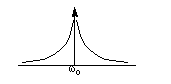
Oscillators exhibit a natural tendency to amplify any noise present near the oscillation frequency. The closer the frequency of the noise is to the oscillation frequency, the greater the amplification. Noise amplified by the oscillator in this manner is referred to as phase noise. Phase noise is extremely important because it is the most significant source of noise in oscillators. In addition, because the phase noise is centered about the oscillation frequency, it can never completely be removed by filtering.
Phase noise can be understood by recognizing that the phase of an oscillator is arbitrary simply because there is no drive signal present to lock to. Any waveform that is a solution to an oscillator can be shifted in time and still be a solution. If a perturbation causes the phase to be disturbed, there is nothing that acts to restore the phase, so it is free to drift without bound. If the perturbation is random noise, the drift takes the form of a random walk. Furthermore, the closer the frequency of perturbation is to the oscillation frequency, the better it couples to the phase and the greater the magnitude of the drift. The perturbation need not come from random noise. It might also couple into the oscillator from other sources, such as the power supplies.
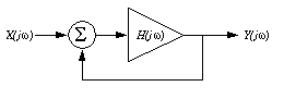
To better understand this phenomenon, consider the feedback oscillator shown. The loop gain of the oscillator is H(jω). X(jw) is taken to represent some perturbation stimulus and Y(jω) is the response of the oscillator to X. The Barkhausen condition for oscillation states that the effective loop gain equals unity and the phase equals 360 degrees at the oscillation frequency ω0 [clarke-hess]. The gain from the perturbation stimulus to the output is
Y(jω) / X(jω) = H(jω) / (1 − H(jω))
which goes to infinity at the oscillation frequency ω0. When the perturbation stimulus is a noise source, the result is phase noise.
The amplification near the oscillation frequency that generates the phase noise is quantified by assuming the loop gain varies smoothly as a function of frequency in this region [razavi96]. If
and the transfer function becomes
Y(j(ω0 + Δω)) / X(j(ω0 + Δω)) ≈ (H(j ω0) + dH/dω Δω) / (1 − H(jω0) − dH/dω Δω).
Because H(jω0) = 1 and dH/dω Δω << 1 in most practical situations, the transfer function reduces to
Y(j(ω0 + Δω)) / X(j(ω0 + Δω)) = -1 / (dH/dω Δω)
Thus, for circuits that contain only white noise sources, the phase noise voltage (or current) is inversely proportional to Δω, while the phase noise power spectral density is proportional 1/Δω2 near the oscillation frequency.
Phase noise is created by a linear phenomenon, the amplification of noise near the carrier frequency that is a natural consequence of the oscillator’s complex pole pair on the jω axis at ω0. In addition, practical oscillators are also strongly nonlinear because they operate in compression. Recall that the loop gain of the oscillator must equal 1 at the oscillation frequency. If the loop gain is less than 1, the oscillation eventually dies out. To ensure the oscillator reliably oscillates even with normal variations in component values, the initial loop gain is always designed to be larger than 1, with the understanding that as the amplitude of the oscillation builds the amplifier goes into compression, which reduces the loop gain. The amplitude stabilizes at the point where the effective loop gain is 1. The nonlinear behavior inherent in practical oscillators results in noise folding. Noise mixes with the oscillation signal and its harmonics and get converted up or down in frequency by one or more multiples of the fundamental frequency. Besides the effect noise folding has on the noise level, it also introduces two noteworthy and easily identifiable artifacts.
First, the phase noise present near the oscillation frequency is mixed up and down, resulting in smaller, but still quite noticeable noise peaks at DC and each harmonic.
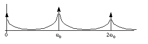
Second, if there are flicker noise sources present in the circuit, the flicker noise mixes up from low frequencies and results in additional noise near the oscillation frequency and its harmonics. Thus, for circuits that contain flicker noise sources, the noise power spectral density is proportional to 1/Δω3 near the oscillation frequency.
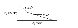
Phase noise is strongly affected by the Q of the oscillator. The higher the Q, the lower the phase noise. To see this, let H(jω) = A(ω) exp(jF(ω)). Then
|Y/X|2 = 1 / {Δω2[(dA/dω)2 + (dΦ/dω)2]}.
Razavi extends the traditional definition of Q to make it more insightful for ring and relaxation oscillators. Open loop Q is
Q = ω0 sqrt{(dA/dω)2 + (dΦ/dω)2} / 2.
In a resonant oscillator, dA/dω = 0 and so the open loop Q reduces to the traditional definition, Q = ω0 / 2(dΦ/dω). For ring and relaxation oscillators, dA/dω and dΦ/dω are of the same order and this new definition is more appropriate. The open loop Q is a measure of how much the closed-loop system opposes variations in the frequency, as seen with
Sample Spectre RF Circuits
The following sections discuss two possible uses for Spectre RF, to simulate
Characterizing a High-Performance Receiver
This receiver was characterized using the sequence of analyses shown in the netlist in Example 3-1 [telichevesky96a]. Each analysis, along with its results, is described in the following sections. The analyses were run on an HP 735/125.
Example 3-1 Netlist Showing the Analyses Run on the Receiver
// compute steady state response to LO only
disableRF alter dev=Prf param=type value=dc
loAlone pss fund=780MHz
// compute transfer functions from all sources to output
freqResponse (out 0) pxf start=20kHz stop=200MHz lin=50
        maxsideband=3
// compute output & input-referred noise, & noise figure
noise pnoise start=2kHz stop=200MHz oprobe=Rl iprobe=Prf
        refsideband=1 maxsideband=15
// compute intermod distortion with LO and 2 input tones
enableRF alter dev=Prf param=type value=sine
interMod pss fund=10MHz swapfile="bigjake" outputtype=both
// compute harmonic distortion with LO and 1 input tone
disable2ndRFtone alter dev=Prf param=ampl2 value=0
harmDisto pss fund=60MHz harms=30
// apply second small signal tone to measure intermod
interModAC pac start=850MHz sidebands=[-15 -13]
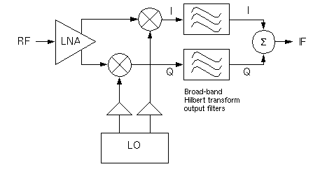
The large RF circuit shown in Figure 3-1 is an image rejection receiver that consists of a low-noise amplifier, a splitting network, two double-balanced mixers, and broad-band Hilbert transform output filter combined with a summing network that is used to suppress the undesired sideband. A limiter in the LO path is used for controlling the amplitude of the LO.
Figure 3-1 Block Diagram for a High-Performance Receiver
The receiver contains 167 bipolar transistors and uses 378 nodes. It is simulated at the circuit level using the Gummel-Poon model for each transistor. It generated 986 equations (largely because of the large number of inductors but also because the internal nodes of the BJTs needed to support their parasitic resistors).
PSS Analysis
This analysis computes the steady-state response of the circuit with only the LO applied. This is a necessary step that allows the use of the periodic small-signal analyses later. The alter statement that precedes the PSS analysis is used to disable the RF input.
Waveforms computed by this analysis are shown in Figure 3-2. The response of the receiver computed by PSS analysis is loAlone at the LO input and it appears in the top half Figure 3-2. The response of the receiver at the output appears in the bottom half Figure 3-2.
Figure 3-2 Response of the High-Performance Receiver for the PSS Analysis
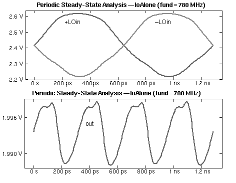
The Spectre RF simulation required about 30 seconds to complete this analysis. The PSS analysis used 200 time points and needed about 25 MB, or about 125 b per equation per time point.
PXF Analysis
The results from the PXF analysis freqResponse are shown in Figure 3-3. Each transfer function from the RF input to the IF output represents a different sideband. Unlike traditional transfer functions as computed by AC analysis, these transfer functions can have inputs and outputs at different frequencies.
The transfer function from the RF input Vrf to the output voltageV(out) appears in the top half of Figure 3-3. The bottom half of Figure 3-3 is an expanded version of the top that clearly shows the conversion due to the ±1 harmonics of the LO.
Figure 3-3 Transfer Function From the Vrf to V(out)
The X axis is labeled with the input frequency (by setting freqaxis to in), although you can also view the transfer functions versus the output frequency (set freqaxis to out). The output frequency range for all of the transfer functions shown is baseband, which is being swept from 20 kHz to 200 lHz. For example, Vrƒ(2) is the transfer function from the second upper sideband to baseband, and finally, Vrƒ(0) is the transfer function from baseband to baseband.
Consider the dip at 700 MHz in Vrƒ(-1), at which point the receiver exhibits 28 dB of attenuation. This implies that a signal from Vrƒ at -700 MHz mixes with the -1st harmonic of the LO and shows up attenuated at the output at
ƒout = -700 MHz + 780 MHz = 80 MHz
Similarly, an 800 MHz signal at the input would mix with the 1st harmonic of the LO and would appear at the output at
ƒout = 800 MHz - 780 MHz = 20 MHz
amplified by 15 dB. This strong asymmetry in the transfer function on either side of the LO is a clear indication that this receiver is designed to suppress the lower sideband.
Figure 3-4 shows the transfer functions to the output voltage, V(out), from Vlo and Vcc. The top half of the figure shows the transfer function to V(out) from the LO input, Vlo. The bottom half of the figure shows the transfer function to V(out) from the power supply, Vcc. This shows how sensitive the output is at the specified range of frequencies to noise on the LO or the power supply at various frequencies.
Figure 3-4 Transfer Functions From Vlo and Vcc to V(out)
Spectre RF simulation required 6 minutes to complete this analysis, which contained 50 frequency points, or roughly 7 seconds per point. It reused the 25 MB of memory allocated in the PSS analysis loAlone.
PNoise Analysis
The PNoise analysis is similar to the traditional noise analysis, except it includes the effect of noise moving from one frequency to another as it mixes with the LO and its harmonics. In this case, the noise measured at the output includes contributions from noise generated at frequencies ƒout ± k ƒLO, where k ≤ 15.
This noise analysis is performed on the detailed periodically varying linearized circuit, and so it includes subtle effects in the calculation. For example, at the points in time where the LO signal is near 0 V, the differential pairs that make up the mixer are balanced and so exhibit a great deal of gain from the LO to the output. Any noise on the LO is greatly magnified at this time. After the LO moves away from 0, the differential pairs saturate and so exhibit a great deal of attenuation from the LO to the output. The faster the LO moves through zero, the less noise is transferred from the LO to the output. This is why switching mixers are preferred over multiplying mixers. This effect is accurately accounted for by the PNoise analysis.
The output noise, input-referred noise, and the noise figure as computed by the PNoise analysis are shown in Figure 3-5. The outpupt noise at V(out) and the input-referred noise from Vrf appear in the top of the figure. The noise figure from Vrf, assuming 50 W source resistance appears in the bottom of the figure. The flicker or 1/f noise of the devices is clearly visible.
Figure 3-5 Output Noise, Input-Referred Noise, and Noise Figure
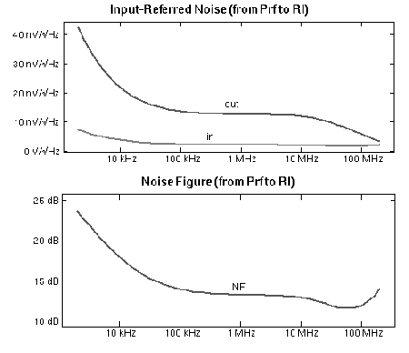
Spectre RF simulation required 8 minutes to complete this analysis, which contained 50 frequency points, or roughly 10 seconds per point. It reused the 25 MB of memory allocated in the PSS analysis loAlone.
PSS Analysis interMod for Intermodulation Distortion
To measure the intermodulation distortion of a mixer, you can apply two tones to the input that are relatively close in frequency. The two tones must be co-periodic with each other and with the LO in order to perform a Fourier analysis. The steady-state response is then found, and the mixer is simulated for a time interval equal to the common period of the three input signals.
In order to compute the steady-state response, you can apply transient analysis until the initial transients decay to negligible levels, or you can apply the PSS analysis. If the transients decay quickly, transient analysis is generally preferred, because it is fast and does not require much memory. Otherwise, PSS analysis is usually preferred.
In this circuit, the LO frequency is 780 MHz and two 25 mV input signals were applied at 840 MHz and 850 MHz. The PSS analysis period was set to 100 ns. A Fourier analysis was performed and 12 harmonics were requested. The nonperiodicity reported by the Fourier analysis was only 61 nV, indicating that if any transients existed, they were very small. The results are shown in Table 3-1.
Table 3-1 Output Spectrum as Computed by PSS Analysis
| Freq | Absolute Level | Relative Level |
|---|---|---|
The third-order intercept point is computed using simple geometric reasoning [kundert95].
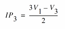
In Equation 3-1,
- V1 is the magnitude of the first fundamental signal at 60 MHz
- V3 is the magnitude of the first IM3 term at 50 MHz
Both voltages are measured in dBV.
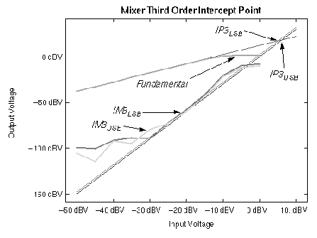
From Table 3-1, V1 = – 19.81 dBV and V3 = –73.03 dBV, which indicates that the intercept point is 6.8 dBV. To confirm this number, the input amplitude was stepped over a range of values, and the amplitude of the fundamental (at 60 MHz) and the third-order intermodulation term (at 50 MHz) were plotted in Figure 3-6. The curves were extrapolated to compute
In Figure 3-6, the third-order intercept point of the receiver was computed by extrapolating actual measurements at small-signal levels. The measured result is either 6 or 7 dBV depending on whether the upper or lower sidebands are used. The IM3 curves bend up at low levels due to small levels of numerical error generated by the simulator. This problem could be reduced at the expense of longer simulations and increased memory requirements by tightening simulator tolerances.
Figure 3-6 Third Order Intercept Point of the Receiver
Spectre RF simulation required 15 minutes to complete the analysis. It used roughly 5,000 timesteps. At 125 b per equation per timestep, PSS would require over 600 MB of swap space to run. The computer used had only 1 GB of free disk space. The swapfile parameter of the PSS analysis was used to direct the simulator to use a conventional file rather than virtual memory to hold the periodically varying linear representation of the circuit. It used 430 MB for the swapfile and 40 MB of virtual memory.
An important thing to keep in mind, especially when reading “PSS harmDisto and PAC interModAC for Intermodulation Distortion”, is that with the approach used in this section, both the simulation time and memory increase in inverse proportion to the difference in frequencies of the two test tones. In this case, the difference was large, and so the problem was tractable. However, if the frequency difference dropped to 1 MHz or below, this approach would have been impractical.
PSS harmDisto and PAC interModAC for Intermodulation Distortion
An alterative approach to computing the intermodulation distortion of the receiver is to apply the LO and only one of the two input test tones during the PSS analysis. Apply the second input tone as a small-signal during a PAC analysis. The benefit to this approach is that the simulation interval used during PSS analysis can be much shorter. In this circuit, if only the 840 MHz RF input and the 780 MHz LO are assumed to be large, then the simulation interval is shortened from 100 ns on the previous analysis to 16.67 ns on this one. That is a factor of 6 improvement. Instead of 15 minutes, the analysis takes 2.5 minutes and 93 MB to compute 787 time points. However, so far only enough information is available to compute the receiver’s harmonic distortion, which is useful in this case because this receiver is broadband. In many cases the receiver is narrow band and so the ability to efficiently compute the intermodulation distortion is very important.
As a second step, apply a small 850 MHz signal and run PAC analysis. Because only one frequency point is needed from the PAC analysis, it is very efficient, requiring only 47 seconds to compute the perturbation to the PSS solution due to the small 850 MHz RF test signal.
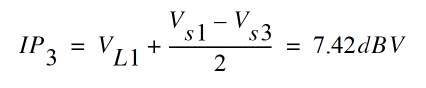
IP3 is computed using VL1, VS1, and VS3, where VL1 = –19.81 dBV is the magnitude at the output of first fundamental-signal at 60 MHz (computed using harmDisto), VS1 = 11.46 dBV is the magnitude at the output of the second fundamental-signal at 70 MHz (computed as the -13th sideband from interModAC), and VS3 = –42.98 dBV is the IM3 term at the output at 50 MHz (computed as the -15th sideband from interModAC).
As shown in Equation 3-2, the third-order intercept point is computed using Equation 3-1.
The 0.3 dB deviation results primarily because the transfer function changes slightly between 840 MHz and 850 MHz, creating some uncertainty in the previous measurement. This uncertainty can be reduced in this measurement by reducing the frequency difference. It can be eliminated by reducing the frequency difference to zero. There is also a small difference between this result and those computed previously that is caused because there is only one large input tone rather than two. This is usually not significant when computing intercept points because the test tones are necessarily rather small. In addition, the various approaches to computing IP3 suffer from small errors in magnitude of the harmonics computed by Spectre RF simulation. These errors can be traced to errors in the waveforms as computed by transient analysis. The errors are quite small relative to the other signals present in the circuit, such as the LO, and are within tolerance. The default tolerances are used. The errors can be reduced considerably by tightening the simulators normal tolerances. The IP3 calculation of Equation 3-2 should be the least sensitive to these errors.
Characterizing a Switched-Capacitor Filter
Spectre RF simulation can simulate switched-capacitor filters at the transistor level. Spectre RF simulation naturally includes second-order effects such as finite bandwidth effects, nonlinear switch resistance effects, charge redistribution effects, slew-rate limiting effects, and back-gate bias effects. It also allows you to include parasitic resistors and capacitors back annotated from the layout in the simulation. Finally, because it simulates at the circuit level, Spectre RF simulation can accurately simulate switched-current filters. These circuits cannot be adequately simulated using traditional switched-capacitor filter simulators, because the imperfections that are second order effects in switched-capacitor circuits play a much more important role in switched-current filters. Most of these effects cannot be included when using traditional switched-capacitor filter simulators.
The switched-capacitor filter being simulated is a 5-pole 2.2 kHz low-pass Elliptic filter. The circuit contains 71 MOSFETs and generates 58 equations. The filter was characterized using the sequence of analyses shown in the following netlist. Each analysis, along with its results, is described in the following sections. The analyses were run on an HP 735/125.
Example 3-2 The Analyses Run on the Switched-Capacitor Filter
// PSS analysis (sets periodic operating point)
clockAlone pss fund=CLOCK_FREQ saveinit=yes readic="%C:r.ic"
        writefinal="%C:r.ic"
// Measure transfer functions
TFin pac stop=10kHz lin=200
// Use PXF to get all transfer functions (including PSR)
unsmpldTFall (out gnd) pxf stop=10kHz lin=200 maxsideband=5
smpldTFall (sout gnd) pxf stop=10kHz lin=200 maxsideband=5
// Measure noise
unsmpldNoise (out gnd) pnoise start=100 stop=25kHz
        maxsideband=25
smpldNoise (sout gnd) pnoise start=100 stop=25kHz
        maxsideband=25
PSS Analysis clockAlone
This analysis computes the steady-state response of the circuit with only the clock applied. The results of this analysis are used to measure the offset voltage at the output of the filter that results from the offset voltage of the op-amps and charge injection from the switches into the integrators. This analysis is also a prerequisite to the periodic small-signal analyses that follow because it sets the periodic operating point.
The PSS analysis, like a conventional transient analysis, starts off from an initial condition. If you do not specify an initial condition, then Spectre RF simulation uses a DC analysis to determine the initial condition. During a DC analysis, the clocks are not operating, so the integrators have no feedback, keeping their outputs stuck at the rails. The initial condition computed during the DC analysis causes the filter to react wildly in transient analysis as shown in Figure 3-7, bouncing off the rails several times before it settles. This results in convergence difficulties during PSS analysis that you can resolve several ways.
One approach that works in this case is to simply specify zero initial conditions for all capacitors in the circuit. This avoids a bad starting point. Another approach that is widely applicable when confronting convergence problems in PSS analysis is to use the tstab parameter to delay the start of the PSS shooting loop. In this example, tstab = 1.5 ms, which implies that transient analysis is performed to at least t = 1.5 ms before the PSS analysis attempts to compute the steady-state solution. Waiting until t = 1.5 ms allows the simulator to get beyond the difficult time when the filter is bouncing off the rails, which results in PSS analysis converging easily.
As shown in Figure 3-7, the transient behavior of an internal node in the filter shows clipping that results from using the DC operation point as the initial condition. The clipping causes convergence problems for PSS analysis. Convergence is easily achieved either by setting tstab = 1.5 ms so that the PSS analysis gets beyond the clipping, or setting the initial conditions on the capacitors to zero.
Figure 3-7 Transient Behavior of an Internal Node
After the steady-state response has been computed, recomputing it is accelerated by saving the final point computed by the PSS analysis and using it as an initial condition for subsequent PSS analyses. (Remember that because the steady-state response is periodic, the final point is the same as the initial point.)
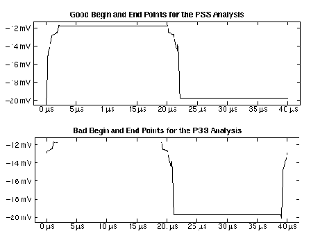
In order to further improve the efficiency of the PSS analysis, the phasing of the clock signals relative to the simulation interval is carefully chosen. It is best to have the simulation interval begin and end at points where the signals are not changing abruptly. For example, the phasing shown in the top half of Figure 3-8 results in convergence in fewer iterations and less time than the phasing shown in the bottom half of the figure. In the top half of the figure, the signal is settled and unchanging immediately prior to the end of the analysis. Contrast this with the situation shown in the lower half of the figure, in which the waveform is changing abruptly at the end point.
Figure 3-8 Choosing Begin and End Points for PSS Analysis
PAC Analysis TFin
The PAC analysis applies a small-signal at the input and computes the response at two outputs. The first output is the normal output of the filter. The signal at this output is continuous in time and includes various imperfections such as glitches and regions of slew-rate limiting and settling. It also contains output from both phases of filter. This output is interesting if the filter is followed with a continuous-time filter. The second output is the normal output after being passed through a sample-and-hold. This models the situation where the filter would be followed by an analog-to-digital converter (ADC) for further processing. In this case, most of the imperfections on the normal output are ignored by the sampling nature of the ADC. Taking into account the sampling nature of the ADC is important when trying to measure the transfer function, the noise, or the distortion of any clocked analog circuit such as a switched-capacitor filter.
With this circuit, only the magnitude and phase of the response at the fundamental frequency are interesting. The small input signal is considered to have unit magnitude and so the transfer functions are computed directly. The transfer functions are shown in Figure 3-9. Notice that the second null is missing from the transfer function of the normal (continuous-time) output. This is a consequence of blending the response from both phases of the filter.
Figure 3-9 Transfer Functions from the Input Voltage to the Outputs
There are two possible outputs, each of which is used in a different application. The first is the normal output of the filter and the second is the normal output after being passed through a sample-and-hold.
The sample-and-hold was implemented in the Verilog-A language and is shown in the following netlist. This sample-and-hold is implemented in such a way that there is no hidden state that would prevent you from using PSS analysis. Both the delay and the aperture must be smaller than the period.
Example 3-3 Netlist Showing Sample-and-Hold Implemented Without Hidden State
module sh (Pout, Nout, Pin, Nin) (period, delay, aperture,
    tc)
node [V,I] Pin, Nin, Pout, Nout;
parameter real period=1 from (0:inf);
parameter real delay=0 from [0:inf);
parameter real aperture=1/100 from (0:inf);
parameter real tc=1/500 from (0:inf);
integer n; real start, stop;
node[V,I] hold;
    analog {
// Determine time aperture begins
        n = ($time() - delay + aperture) / period + 0.5;
        start = n*period + delay - aperture;
        $break_point( start );
// Determine time aperture ends
        n = ($time() - delay) / period + 0.5;
        stop = n*period + delay;
        stop = n*period + delay;
// Implement switch with effectively 1 Ohm series resistance
        if (($time() > start) && ($time() <= stop))
            I(hold) <- V(hold) - V(Pin,Nin);
        else
            I(hold) <- 1.0e-12 * (V(hold) - V(Pin,Nin));
// Implement capacitor with an effective capacitance of tc
I(hold) <- tc * dot(V(hold));
// Buffer output
V(Pout,Nout) <- V(hold);
// Control time step tightly during aperture
        if (($time() >= start) && ($time() <= stop))
            $bound_step( tc );
        else
            $bound_step( period / 5 );
    }
}
PXF Analyses unsmpldTFall and smpldTFall
These analyses directly compute the transfer function from all sources to either the unsampled or sampled output. They differ from the PAC analysis TFin in that they compute transfer functions from all sources to a single output rather than the transfer functions to all outputs from a single input. They are also about 50% slower than the PAC analysis. They are useful when measuring the ability of the filter to reject unwanted signals on the input, the clock, and on the supplies.
PNoise Analyses unsmpldNoise and smpldNoise
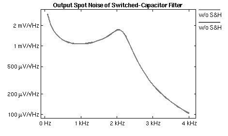
These analyses compute the total spot noise as a function of frequency at the sampled and unsampled outputs. The results are shown in Figure 3-10. They include noise folding (noise being converted down from sidebands of the clock by the sampling nature of the switched-capacitor filter).
Figure 3-10 Noise Response of Switched Capacitor Including Noise Folding
References
Return to top