|
level=1
|
Model level.
|
|
paramchk=0
|
Model parameter checking selector.
|
|
version=1
|
Model version.
|
|
subversion=0
|
Model subversion.
|
|
revision=2
|
Model revision.
|
|
tmin=100 degC
|
Minimum ambient temperature.
|
|
tmax=500 degC
|
Maximum ambient temperature.
|
|
gmin=1e-12 S
|
Minimum parasitic conductance.
|
|
imax=1 A
|
Current at which to linearize diode currents.
|
|
scale=1
|
Scale factor for instance geometries.
|
|
shrink=0 %
|
Shrink percentage for instance geometries.
|
|
rthresh=0.001 Ω
|
Threshold to switch end resistance to V=I*R form.
|
|
type=n
|
JFET type: +1=n-body and -1=p-body. Possible values are n and p.
|
|
swbgmos=0
|
Switch to indicate bottom gate type: 0=pn-junction and 1=mos.
|
|
swtgmos=0
|
Switch to indicate top gate type: 0=pn-junction and 1=mos.
|
|
swgeo=1
|
Switch for geometry modeling: 0=local and 1=global.
|
|
swgdep=1
|
Switch for geometry mapping basis: 0=drawn and 1=effective.
|
|
tnom=27 degC
|
Nominal (reference) temperature.
|
|
lmin=0.0 m
|
Minimum allowed drawn length.
|
|
lmax=9e+09 m
|
Maximum allowed drawn length.
|
|
wmin=0.0 m
|
Minimum allowed drawn width.
|
|
wmax=9.9e+09 m
|
Maximum allowed drawn width.
|
|
jmax=1e+08 A/m
|
Maximum current density.
|
|
vmax=9.9e09 V
|
Maximum drain or source voltage w.r.t. either gate.
|
|
tminclip=(-100) degC
|
|
|
Clip minimum temperature.
|
|
tmaxclip=800 degC
|
Clip maximum temperature.
|
|
grpo=1e-12
|
Minimum body conductance in pinch-off (ratio w.r.t. Vc=0).
|
|
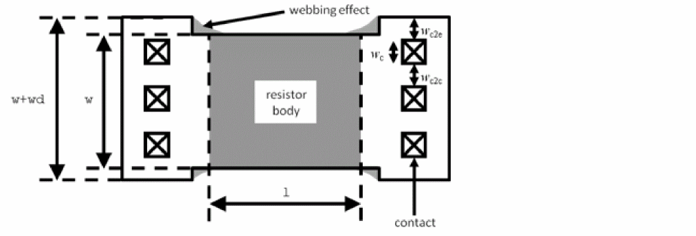
xw=0 m
|
Width offset (total).
|
|
nwxw=0 m
|
Narrow width offset correction coefficient.
|
|
wexw=0 m
|
Webbing effect width offset correction coefficient (for dogboned devices).
|
|
fdrwo=1e-06 m
|
Finite doping width offset reference width.
|
|
fdxwo=0 m
|
Finite doping width offset width value for wide devices.
|
|
xl=0 m
|
Length offset (total).
|
|
xlw=0 m
|
Width dependence of length offset.
|
|
dxlsat=0 m
|
Additional length offset for velocity saturation calculation.
|
|
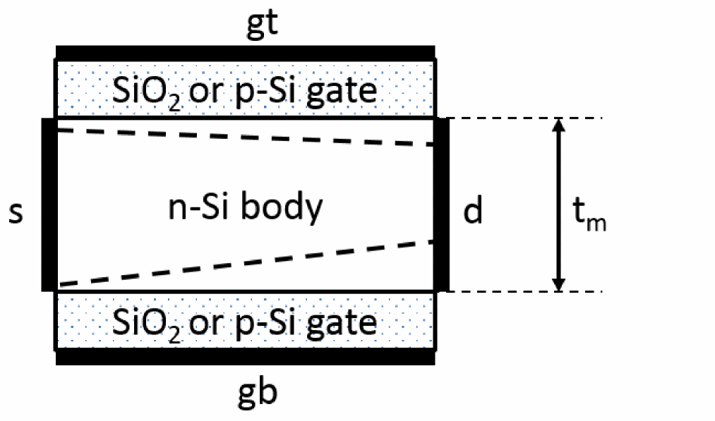
tm=5e-07 m
|
Channel thickness (metallurgical).
|
|
nc=1e+23 /m^3
|
Channel doping concentration.
|
|
nb=1e+22 /m^3
|
Bottom-gate doping concentration.
|
|
toxb=4e-07 m
|
Bottom-gate oxide thickness.
|
|
vfbb=0 V
|
Bottom-gate flatband voltage.
|
|
nt=1e+26 /m^3
|
Top-gate doping concentration.
|
|
toxt=4e-07 m
|
Top-gate xide thickness.
|
|
vfbt=0 V
|
Top-gate flatband voltage.
|
|
dfb=0.01 /V^0.5
|
Bottom-gate depletion factor (overrides calculation if specified).
|
|
dfbo=0.01 /V^0.5
|
dfb Geometry-independent part.
|
|
dfbl=0
|
dfb 1/l coefficient.
|
|
dfble=1
|
dfb 1/l exponent.
|
|
dfbw=0
|
dfb 1/w coefficient.
|
|
dfbwe=1
|
dfb 1/w exponent.
|
|
dfblw=0
|
dfb 1/(l*w) coefficient.
|
|
dfbfac=1
|
dfb adjustment coefficient.
|
|
psirb=2 V
|
Bottom-gate depletion potential (overrides calculation if specified).
|
|
psirbo=2 V
|
psirb Geometry-independent part.
|
|
psirbl=0
|
psirb 1/l coefficient.
|
|
psirble=1
|
psirb 1/l exponent.
|
|
psirbw=0
|
psirb 1/w coefficient.
|
|
psirbwe=1
|
psirb 1/w exponent.
|
|
psirblw=0
|
psirb 1/(l*w) coefficient.
|
|
psirbfac=1
|
psirb adjustment coefficient.
|
|
dft=0.01 /V^0.5
|
Top-gate depletion factor (overrides calculation if specified).
|
|
dfto=0.01 /V^0.5
|
dft Geometry-independent part.
|
|
dftl=0.0
|
dft 1/l coefficient.
|
|
dftle=1.0
|
dft 1/l exponent.
|
|
dftw=0.0
|
dft 1/w coefficient.
|
|
dftwe=1.0
|
dft 1/w exponent.
|
|
dftlw=0.0
|
dft 1/(l*w) coefficient.
|
|
dftfac=1.0
|
dft adjustment coefficient.
|
|
psirt=2.0 V
|
Top-gate depletion potential (overrides calculation if specified).
|
|
psirto=2.0 V
|
psirt Geometry-independent part.
|
|
psirtl=0.0
|
psirt 1/l coefficient.
|
|
psirtle=1.0
|
psirt 1/l exponent.
|
|
psirtw=0.0
|
psirt 1/w coefficient.
|
|
psirtwe=1.0
|
psirt 1/w exponent.
|
|
psirtlw=0.0
|
psirt 1/(l*w) coefficient.
|
|
psirtfac=1.0
|
psirt adjustment coefficient.
|
|
mu0=0.05 m^2/V/s
|
Low-field mobility
|
|
r0=100 Ohm
|
Zero-bias resistance.
|
|
rsh0=100 Ohm/sq
|
Zero-bias sheet resistance (overrides calculation if specified).
|
|
rzd=100 Ohm
|
Zero-depletion resistance.
|
|
rshzd=100 Ohm/sq
|
Zero-depletion sheet resistance (overrides calculation if specified).
|
|
rcs=0 Ohm
|
Source contact resistance.
|
|
rcd=0 Ohm
|
Drain contact resistance.
|
|
rc=0 Ohm
|
Resistance per contact.
|
|
rcw=0 Ohm
|
Width adjustment for contact resistance.
|
|
diblb=0
|
Bottom-gate dibl.
|
|
diblbl=0
|
diblb l dependence coefficient.
|
|
diblt=0
|
Top-gate dibl.
|
|
dibltl=0
|
diblt l dependence coefficient.
|
|
diblle=1
|
dibl l dependence exponent.
|
|
diblv=0.1 V
|
dibl voltage offset.
|
|
dible=0.5
|
dibl voltage exponent.
|
|
clm1=0
|
clm linear component.
|
|
clm1l=0
|
clm1 l dependence coefficient.
|
|
clm1le=1
|
clm1 l dependence exponent.
|
|
clm1c=0 /V
|
clm1 V(gx) dependence coefficient.
|
|
clm2=0
|
clm nonlinear component.
|
|
clm2l=0
|
clm2 l dependence coefficient.
|
|
clm2le=1
|
clm2 l dependence exponent.
|
|
clm2v=0.1 V
|
clm2 voltage offset.
|
|
clm2e=0.5
|
clm2 voltage exponent.
|
|
ats=0.0 V
|
Saturation smoothing parameter.
|
|
atso=0 V
|
ats Geometry-independent part.
|
|
atsl=0 V
|
ats 1/l coefficient.
|
|
axs=0
|
Second saturation smoothing parameter.
|
|
axso=0
|
axs Geometry-independent part.
|
|
axsl=0
|
axs 1/l coefficient.
|
|
nspo=1
|
Slope parameter under source pinch-off.
|
|
nspoo=1
|
nspo Geometry-independent part.
|
|
nspol=0
|
nspo 1/l coefficient.
|
|
nspole=1
|
nspo 1/l exponent.
|
|
nspow=0
|
nspo 1/w coefficient.
|
|
nspowe=1
|
nspo 1/w exponent.
|
|
nspolw=0
|
nspo 1/(l*w) coefficient.
|
|
alphab=0 /V
|
Bottom-gate impact ionization current prefactor.
|
|
alphabo=0 /V
|
alphab Geometry-independent part.
|
|
alphabl=0 /V
|
alphab 1/l coefficient.
|
|
alphat=0 /V
|
Top-gate impact ionization current prefactor.
|
|
alphato=0 /V
|
alphat Geometry-independent part.
|
|
alphatl=0 /V
|
alphat 1/l coefficient.
|
|
beta=10 V
|
Impact ionization current exponent for both gates.
|
|
mumb=0 /V
|
Bottom-gate mobility modulation coefficient.
|
|
mumboff=0 V
|
Bottom-gate mobility modulation voltage offset.
|
|
mumbs=1
|
Bottom-gate mobility modulation smoothing parameter.
|
|
mumbe=1
|
Bottom-gate mobility modulation exponent.
|
|
mumbo=0 /V
|
mumb Geometry-independent part.
|
|
mumbl=0
|
mumb 1/l coefficient.
|
|
mumbw=0
|
mumb 1/w coefficient.
|
|
mumblw=0
|
mumb 1/(l*w) coefficient.
|
|
mumt=0 /V
|
Top-gate mobility modulation coefficient.
|
|
mumtoff=0 V
|
Top-gate mobility modulation voltage offset.
|
|
mumts=1
|
Top-gate mobility modulation smoothing parameter.
|
|
mumte=1
|
Top-gate mobility modulation exponent.
|
|
mumto=0 /V
|
mumt Geometry-independent part.
|
|
mumtl=0
|
mumt 1/l coefficient.
|
|
mumtw=0
|
mumt 1/w coefficient.
|
|
mumtlw=0
|
mumt 1/(l*w) coefficient.
|
|
mumii1=0 /V^2
|
Linear impact ionization mobility modulation coefficient.
|
|
mumii2=0 /V^4
|
Quadratic impact ionization mobility modulation coefficient.
|
|
vcrit=4 V
|
Velocity saturation critical voltage.
|
|
ecrit=4e+06 V/m
|
Velocity saturation critical field.
|
|
vcorn=0.4 V
|
Velocity saturation corner voltage.
|
|
ecorn=4e+05 V/m
|
Velocity saturation corner field.
|
|
du=0.02
|
Mobility reduction at ecorn.
|
|
voffspo=0
|
Source pinchoff offset (number of nspo*phi_t).
|
|
moffspo=1
|
Source pinchoff smoothing factor.
|
|
gth=0 W/K
|
Thermal conductance.
|
|
gtho=0 W/K
|
gth Geometry-independent part.
|
|
gthp=0 W/K/m
|
gth perimeter component.
|
|
gtha=0 W/K/m2
|
gth area component.
|
|
gthc=0 W/K
|
gth contact component.
|
|
cth=0 s W/K
|
Thermal capacitance.
|
|
ctho=0 s W/K
|
cth Geometry-independent part.
|
|
cthp=0 s W/K/m
|
cth perimeter component.
|
|
ctha=0 s W/K/m2
|
cth area component.
|
|
cthc=0 s W/K
|
cth contact component.
|
|
fc=0.9
|
Ddepletion capacitance linearization factor.
|
|
isab=0 A/m2
|
Bottom-gate diode saturation current per unit area.
|
|
nab=1
|
Bottom-gate ideality factor for isa.
|
|
cab=0 F/m2
|
Bottom-gate fixed capacitance per unit area.
|
|
cjab=0 F/m2
|
Bottom-gate depletion capacitance per unit area.
|
|
pab=0.75 V
|
Bottom-gate built-in potential for cja.
|
|
mab=0.33
|
Bottom-gate grading coefficient for cja.
|
|
ajab=-0.5 V
|
Bottom-gate smoothing parameter for cja.
|
|
ispb=0 A/m
|
Bottom-gate diode saturation current per unit perimeter.
|
|
npb=1
|
Bottom-gate ideality factor for isp.
|
|
cpb=0 F/m
|
Bottom-gate fixed capacitance per unit perimeter.
|
|
cpb2=0 F/m
|
Bottom-gate fixed capacitance per unit perimeter (2nd component).
|
|
cjpb=0 F/m
|
Bottom-gate depletion capacitance per unit perimeter.
|
|
ppb=0.75 V
|
Bottom-gate built-in potential for cjp.
|
|
mpb=0.33
|
Bottom-gate grading coefficient for cjp.
|
|
ajpb=-0.5 V
|
Bottom-gate smoothing parameter for cjp.
|
|
ttb=0 s
|
Bottom-gate transit time for diffusion charge.
|
|
vbvb=0 V
|
Bottom-gate breakdown voltage.
|
|
nbvb=1
|
Bottom-gate ideality factor for breakdown current.
|
|
isat=0 A/m2
|
Top-gate diode saturation current per unit area.
|
|
nat=1
|
Top-gate ideality factor for isa.
|
|
cat=0 F/m2
|
Top-gate fixed capacitance per unit area.
|
|
cjat=0 F/m2
|
Top-gate depletion capacitance per unit area.
|
|
pat=0.75 V
|
Top-gate built-in potential for cja.
|
|
mat=0.33
|
Top-gate grading coefficient for cja.
|
|
ajat=-0.5 V
|
Top-gate smoothing parameter for cja.
|
|
ispt=0 A/m
|
Top-gate diode saturation current per unit perimeter.
|
|
npt=1
|
Top-gate ideality factor for isp.
|
|
cpt=0 F/m
|
Top-gate fixed capacitance per unit perimeter.
|
|
cpt2=0 F/m
|
Top-gate fixed capacitance per unit perimeter (2nd component).
|
|
cjpt=0 F/m
|
Top-gate depletion capacitance per unit perimeter.
|
|
ppt=0.75 V
|
Top-gate built-in potential for cjp.
|
|
mpt=0.33
|
Top-gate grading coefficient for cjp.
|
|
ajpt=-0.5 V
|
Top-gate smoothing parameter for cjp.
|
|
ttt=0 s
|
Top-gate transit time for diffusion charge.
|
|
vbvt=0 V
|
Top-gate breakdown voltage.
|
|
nbvt=1
|
Top-gate ideality factor for breakdown current.
|
|
ibv=1e-06 A
|
Current at breakdown.
|
|
kfn=0 m2
|
Flicker noise coefficient.
|
|
afn=2
|
Flicker noise current exponent.
|
|
bfn=1
|
Flicker noise 1/f exponent.
|
|
swfngeo=0
|
Switch for flicker noise geometry calculation: 0=drawn and 1=effective.
|
|
tc1psirb=0 /K
|
psirb linear TC.
|
|
tc2psirb=0 /K2
|
psirb quadratic TC.
|
|
tc1psirt=0 /K
|
psirt linear TC.
|
|
tc2psirt=0 /K2
|
psirt quadratic TC.
|
|
tc1=0 /K
|
Resistance linear TC.
|
|
tc2=0 /K2
|
Resistance quadratic TC.
|
|
tc1o=0 /K
|
tc1 Geometry-independent part.
|
|
tc2o=0 /K2
|
tc2 Geometry-independent part.
|
|
tc1w=0 m/K
|
tc1 1/w coefficient.
|
|
tc2w=0 m/K2
|
tc2 1/w coefficient.
|
|
tc1l=0 m/K
|
tc1 1/l coefficient.
|
|
tc2l=0 m/K2
|
tc2 1/l coefficient.
|
|
tc1lw=0 m2/K
|
tc1 1/(l*w) coefficient.
|
|
tc2lw=0 m2/K2
|
tc2 1/(l*w) coefficient.
|
|
tsl=0 /K
|
Slope of resistance change compared to temperature at low temperature.
|
|
tsh=0 /K
|
Slope of resistance change compared to temperature at high temperature.
|
|
tsct=100 degC
|
Critical temperature where resistance change slope goes from tsl to tsh.
|
|
tssm=10 degC
|
Resistance change slope smoothing parameter.
|
|
tslo=0 /K
|
tsl Geometry-independent part.
|
|
tsho=0 /K
|
tsh Geometry-independent part.
|
|
tscto=100 degC
|
tsct Geometry-independent part.
|
|
tssmo=10 degC
|
tssm Geometry-independent part.
|
|
tslw=0 m/K
|
tsl 1/w coefficient.
|
|
tshw=0 m/K
|
tsh 1/w coefficient.
|
|
tsctw=0 m degC
|
tsct 1/w coefficient.
|
|
tssmw=0 m degC
|
tssm 1/w coefficient.
|
|
tsll=0 m/K
|
tsl 1/l coefficient.
|
|
tshl=0 m/K
|
tsh 1/l coefficient.
|
|
tsctl=0 m degC
|
tsct 1/l coefficient.
|
|
tssml=0 m degC
|
tssm 1/l coefficient.
|
|
tsllw=0 m2/K
|
tsl 1/(l*w) coefficient.
|
|
tshlw=0 m2/K
|
tsh 1/(l*w) coefficient.
|
|
tsctlw=0 m2 degC
|
tsct 1/(l*w) coefficient.
|
|
tssmlw=0 m2 degC
|
tssm 1/(l*w) coefficient.
|
|
tc1rc=0 /K
|
Contact resistance linear TC.
|
|
tc2rc=0 /K2
|
Contact resistance quadratic TC.
|
|
xbeta=0
|
Exponent for impact ionization current exponent temperature dependence.
|
|
tegth=0
|
Thermal conductance temperature exponent.
|
|
xvsat=0
|
Exponent for saturation velocity temperature dependence.
|
|
xvsato=0
|
xvsat Geometry-independent part.
|
|
xvsatl=0
|
xvsat 1/l coefficient.
|
|
xvsatle=1
|
xvsat 1/l exponent.
|
|
ea=1.12 V
|
Activation voltage for diode temperature dependence.
|
|
xis=3
|
Exponent for diode temperature dependence.
|
|
tc1vbvb=0 /K
|
Breakdown voltage linear TC (bottom gate).
|
|
tc2vbvb=0 /K2
|
Breakdown voltage quadratic TC (bottom gate).
|
|
tc1nbvb=0 /K
|
Breakdown ideality factor linear TC (bottom gate).
|
|
tc1vbvt=0 /K
|
Breakdown voltage linear TC (top gate).
|
|
tc2vbvt=0 /K2
|
Breakdown voltage quadratic TC (top gate).
|
|
tc1nbvt=0 /K
|
Breakdown ideality factor linear TC (top gate).
|
|
tc1kfn=0 /K
|
Flicker noise coefficient linear TC.
|
|
nsig_rsh=0
|
Number of standard deviations of global variation for rsh.
|
|
nsig_w=0
|
Number of standard deviations of global variation for w.
|
|
nsig_l=0
|
Number of standard deviations of global variation for l.
|
|
sig_rsh=0 %
|
Global variation standard deviation for rsh (relative).
|
|
sig_w=0 m
|
Global variation standard deviation for w (absolute).
|
|
sig_l=0 m
|
Global variation standard deviation for l (absolute).
|
|
smm_rsh=0 %m
|
Local variation standard deviation for rsh (relative).
|
|
smm_w=0 m^1.5
|
Local variation standard deviation for w (absolute).
|
|
smm_l=0 m^1.5
|
Local variation standard deviation for l (absolute).
|
|
swmmgdep=0
|
Switch for mismatch geometry calculation: 0=drawn and 1=effective.
|
|
swnoise=1
|
Switch to include noise: 0=no and 1=yes.
|
|
swet=1
|
Switch to include self-heating: 0=no and 1=yes.
|
|
swlin=0
|
Switch to force linearity: 0=no and 1=yes.
|
|
swmman=0
|
Switch to enable mismatch analysis: 0=no and 1=yes.
|
|
tref (degC)
|
Alias of tnom.
|
|
tr (degC)
|
Alias of tnom.
|
|
compatible=spectre
|
Encourage device equations to be compatible with a foreign simulator.
Possible values are spectre, spice2, spice3, cdsspice, spiceplus, eldo, sspice, mica, and pspice.
|