Reference
Model Equations
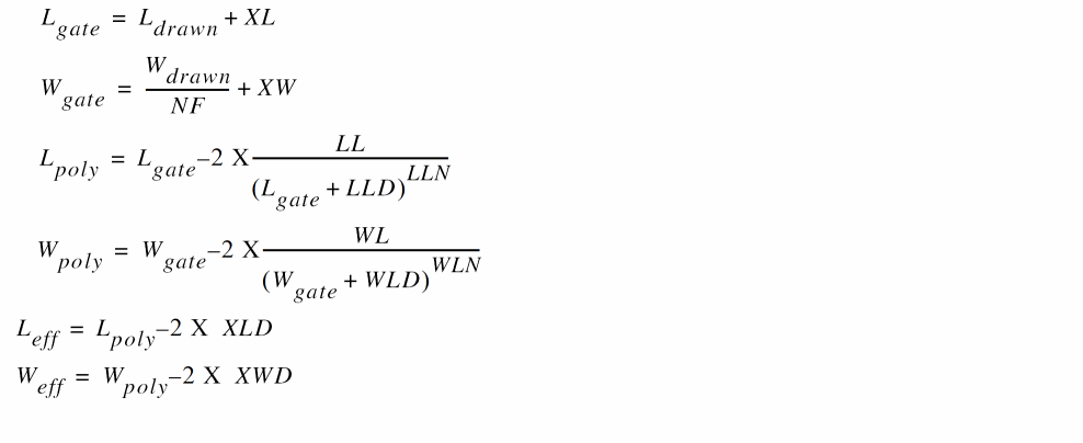
Effective Length and Width
Lgate and Wgate are the gate length and gate width. They are calculated from the gate drawn length and width.
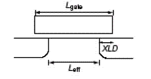
where XLD and XWD account for the overlaps of source/drain contact and gate oxide. LL, LLD, LLN, WL, WLD, and WLN are further model parameters for including Lgate or Wgate dependencies on Leff and Weff.
Figure -2
Cross section of the device
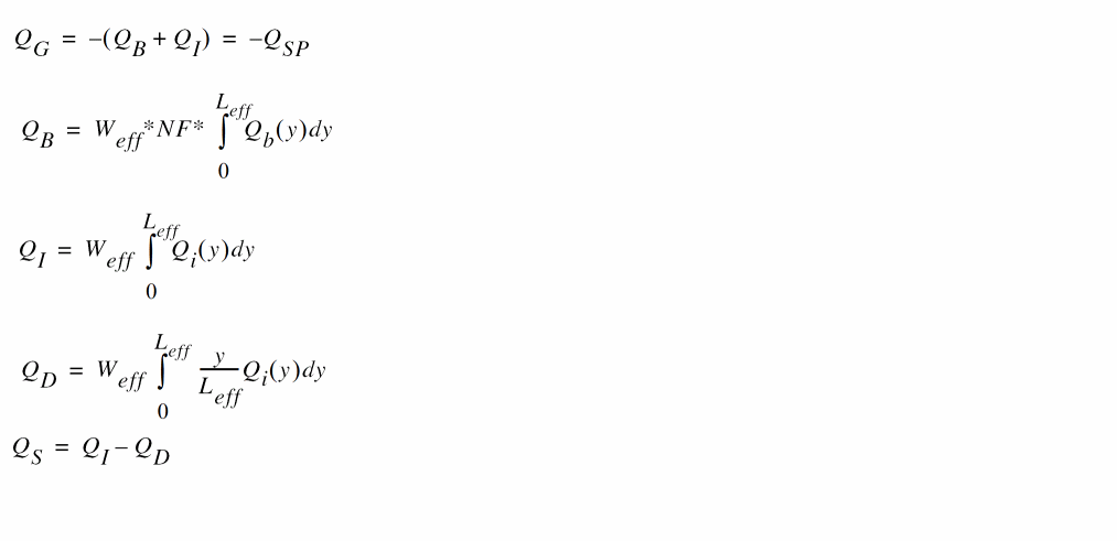
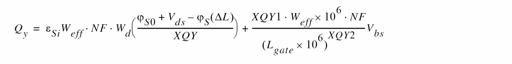
Charge
All device characteristics are determined on the basis of the charge control by applied voltages and by expressing the MOSFET charges as functions of the surface potentials. Under the charge-sheet approximation the charges on the four MOSFET terminals QG(gate), QB (bulk), QD (drain), and QS (source), are described as:
where QI is the inversion charge, QSP is the space charge, and y is the position along the channel. Leff and 0 are the channel-end positions at the drain side and the source side, respectively.
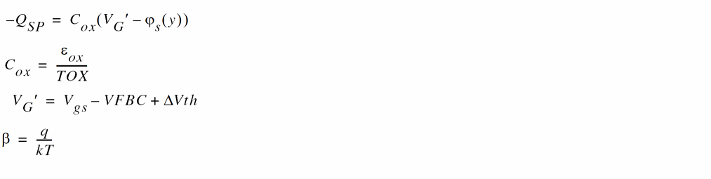
By applying the Gauss law, the space charge density QSP is derived from the Poisson equation.
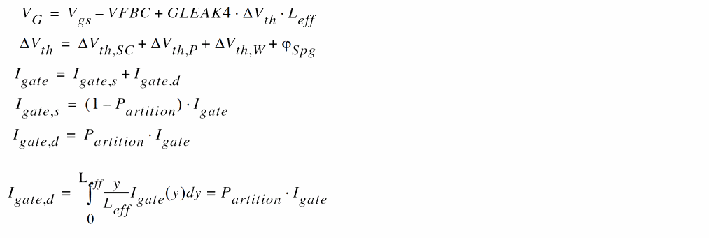
where VFBC is the at-band voltage, TOX is the physical gate-oxide thickness, and ΔVth is the threshold voltage shift in comparison to the threshold voltage of a long-channel transistor. The electron charge is denoted by q, and εsi and Nsub are the silicon permittivity and the substrate impurity concentration, respectively. The Boltzmann constant and the lattice temperature in Kelvin are k and T, respectively.
The quasi-Fermi potential φf (f) preserves the following relationship:
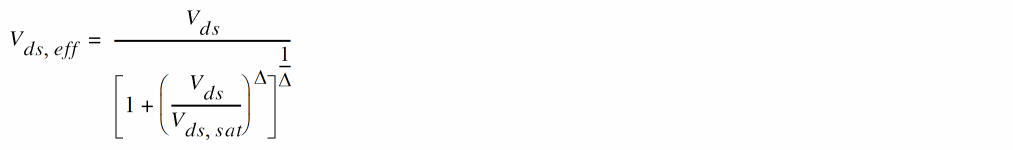
for CODDLT=1 (default):
for CODDLT=0 (previous model):
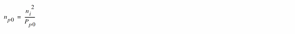
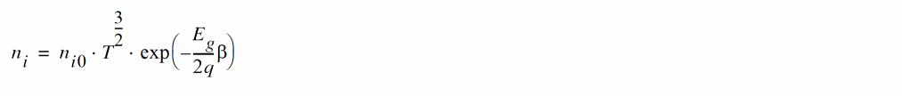
The electron concentration at equilibrium condition np0 is
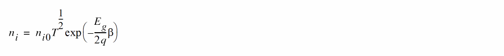
where the intrinsic carrier concentration ni is
pp0 is approximated to be Nsub, and Eg describes the temperature dependence of the bandgap.
The Poisson equation and the Gauss law are used to derive the inversion charge and bulk charge related charge-density equations under the assumption of a homogeneous substrate impurity distribution as
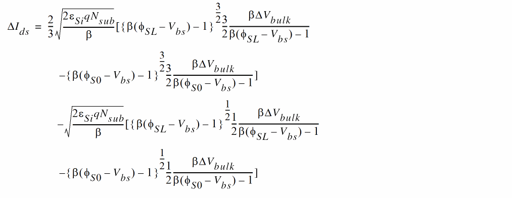
Drain Current
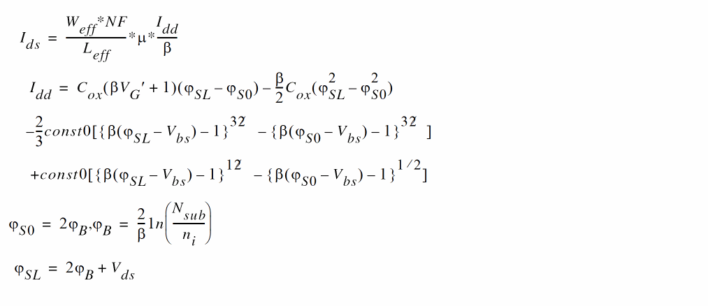
Under gradual-channel approximation with further approximations of an idealized gate structure and uniform channel doping, the drift-diffusion approximation describes the drain current Ids as:
The description for the long-channel case is obtained as:
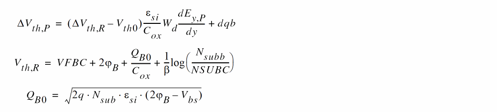
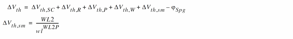
Threshold Voltage Shift
Different from the drift approximation, the drift-diffusion approximation does not require a threshold voltage parameter Vth for describing device performances. The MOSFET device parameters, such as the oxide thickness TOX and the substrate doping concentration NSUBC determine the complete MOSFET behavior including the subthreshold characteristics automatically and consistently. The measured Vth is influenced by various phenomena, such as the short-channel effects, which cause a reduction of Vth for short-channel transistors in comparison to long-channel transistors as shown in Fig. 5. This so-called ΔVth roll-off is dependent on the technology applied for MOSFET fabrication. Therefore, HiSIM can derive many detailed information on the MOSFET fabrication technology, which is relevant for modeling device characteristics, from the Vth changes (ΔVth) as a function of gate length (Lgate). The modeled ΔVth is incorporated in the φS iteration, and can be viewed as consisting of two main effects or components:
-
The short-channel effect: ΔVth,SC
-
The reverse-short-channel effect: ΔVth,R and ΔVth,P
The separation into these components is shown below:
Short-Channel Effect
Four important phenomena are observed:
-
Reduction of Vth for reduced Lgate
-
Vth dependence on Vds
-
Reduction of the body effect
-
Increase of the subthreshold swing, which is often not obvious for the normal case of fabrication technologies. Recent advanced technologies utilize aggressive scaling, which induces observable subthreshold degradation.
where Wd is the depletion-layer thickness written as
dEy/dy is derived with model parameters in the form
Reverse-Short-Channel Effects
Impurity concentration inhomogeneity in the direction vertical to the channel (Retrograded Implantation)
where BS1 represents the strength of the deviation and BS2 is the starting value of Vbs where the deviation becomes visible.
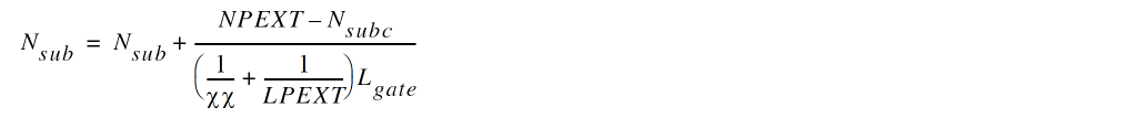
Impurity concentration inhomogeneity in the lateral direction parallel to the channel (Pocket Implantation)
where
CORECIP = 1 for Accurate Reciprocity Calculation of Capacitances
The model CORECIP enables accurate calculation of the capacitance reciprocity. If CORECIP = 1 is selected, the Vds dependence is moved to the puchthrough model described in the next section. Accordingly, model parameters SC2,SC4,SCP2 and SCP4 must be set to zero, and PT2 and PT4 activated.
Short Channel Effects
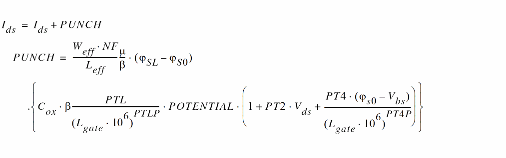
Punchthrough Effect
The origin of the punchthrough effect is the bipolar effect through source, substrate, and drain.The effect is described by a power function of the potential difference instead of the exponential function as
The final drain current Ids is written
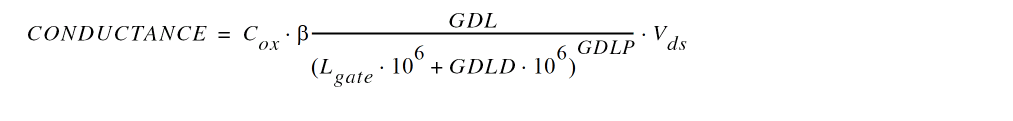
Channel Conductance
The high field under the saturation condition causes the pinch-off region and the current flows away from the surface. This effect is considered as the lateral-field-induced charge for the capacitance. The simplified formulation is applied to consider the effect as
Pocket Impurity Concentration Reduction
If the gate length becomes shorter, the pocket-impurity concentration may become lower than for long channels. This effect is modeled as:
Depletion Effect of the Gate Poly-Si
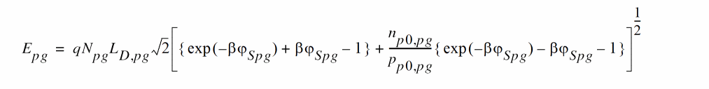
Carrier depletion in the gate poly-Si occurs due to the relatively low impurity concentration of the poly-Si in the region above the gate-oxide. Nevertheless, this concentration is usually much higher than the impurity concentration in the substrate. Therefore, carrier depletion in the poly-Si near the gate-oxide interface starts after the formation of the inversion layer in the substrate. For modeling the gate poly-Si depletion a physical model parameter, namely the impurity concentration in the gate poly-Si (Npg), is introduced.
Quantum-Mechanical Effects
The main quantum-mechanical phenomenon, which has to be included into a MOSFET model for circuit simulation, is the repulsion of the channel's carrier-density peak into the substrate away from the surface. This can be described phenomenologically by an increased effective oxide thickness Tox. Two major approximations are introduced to derive a simple set of equations for Tox: First, a triangular potential perpendicular to the channel is approximated and second, carriers are assumed to occupy only the lowest quantized energy level. The resulting effective oxide thickness Tox can be written as:
For HiSIM2.5
For HiSIM2.5.1
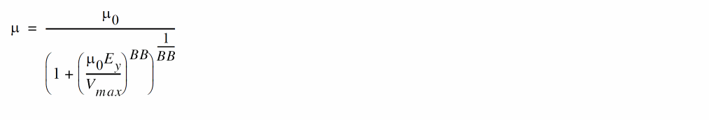
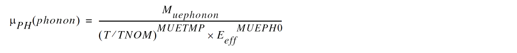
Mobility Model
Here Eeff is the effective field normal to the surface and is written as:
Here Eeff is the effective field normal to the surface and is written as
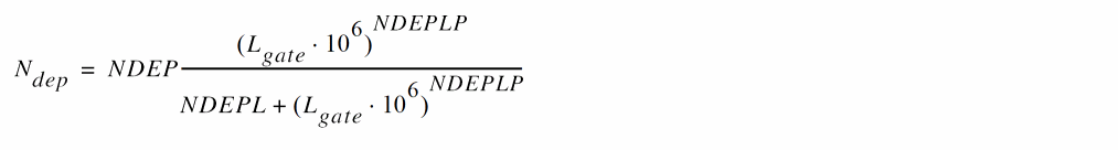
where Ndep considers the gate length dependence with two model parameters NDEPL and NDEPLP as:
The mobility preserves the following conditions:
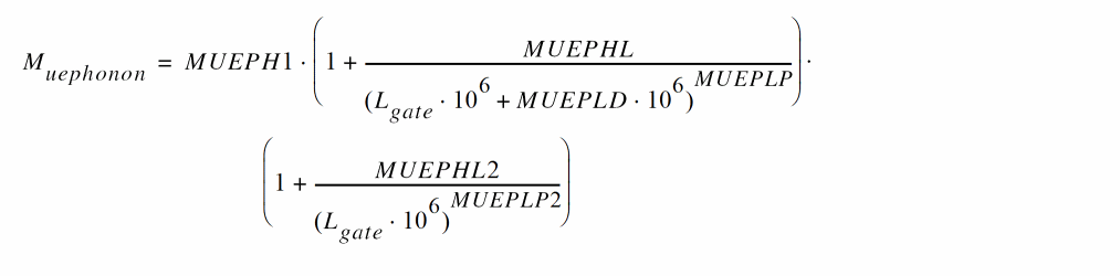
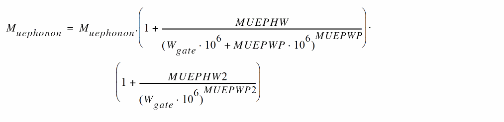
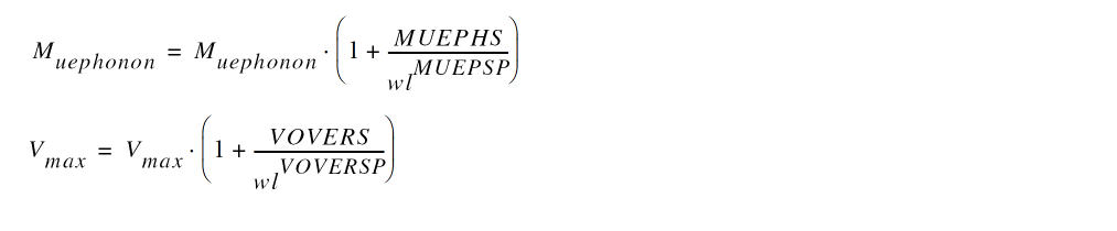
Due to the carrier ow at increasing distance from the surface with reducing Lgate, the electric field experienced by the carriers is different from the field in the long Lgate case. This results in a modification of Muephonon, which is modeled as:
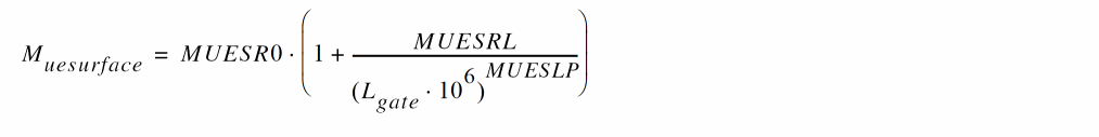
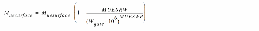
The surface roughness co-efficient Muesurface is modelled to have a similar channel length dependence written as:
The high field mobility is modeled as:
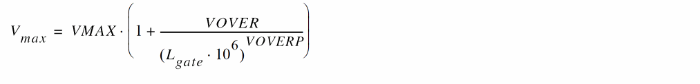
where the maximum velocity Vmax is temperature dependent. Vmax should be the maximum electron-saturation velocity (' 1_107cm=s), which is exceeded at reduced Lgate. This is called velocity overshoot, and is included in the mobility model in the following manner:
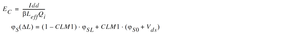
Channel-Length Modulation
The gradual-channel approximation is applied to derive analytical equations for describing device characteristics. However, this approximation is not valid for large Vds causing the pinch-off phenomenon in the channel. Without taking into account the pinch-off phenomenon, the calculated channel conductance gds enters abruptly into the saturation condition. To include the pinch-off phenomenon in HiSIM, we apply the conventional method of modeling the pinch-off region (ΔL) separately from the rest of the channel.
where
and Ec is the electric field at y=0’.
The above equation can be simplified as follows:
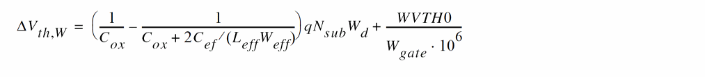
Narrow Channel Effects
Threshold Voltage Modification
where WVTH0 is the parameter for including the basic width dependence and
Here, Tfox is the thickness of the oxide at the trench edge, and WFC is the model parameter for including the edge-fringing-capacitance effects.
Mobility Change
Transistor Leakage due to Shallow Trench Isolation (STI): Hump in Ids
The shallow trench isolation induces also an undesired hump in the subthreshold region of the Ids-Vgs characteristics. This is due to an increased electric field at the edge of the trench. At this trench edge, the impurity concentration as well as the oxide thickness are different from the MOSFET middle position along the width direction. Therefore, the surface potential values are expected to be different at the trench edge and are found to cause a Vth reduction there. Thus a MOSFET leakage current occurs at these edges, which is smaller than the main MOSFET. The leakage current equation is written as:
where WSTI determines the width of the high-field region.
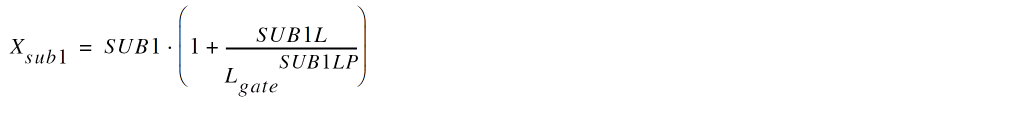
Small Geometry
Small size devices do not show the same scaling characteristic as long-channel or wide-channel devices, but deviate significantly. The reason is mainly due to the resolution inaccuracy of the lithography. The small geometry effects are modeled first as the threshold voltage shift
The mobility modification due to the small device geometry is also modeled in the phonon scattering as
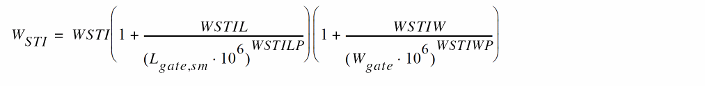
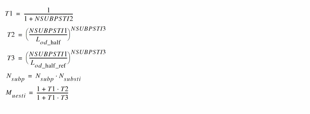
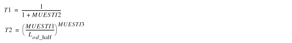
Effects of the Source/Drain Diffusion Length for Shallow Trench Isolation (STI) Technologies
The diffusion length, LOD between MOSFET gate and STI edge affects the MOSFET characteristics.
where
where
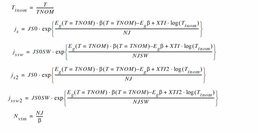
Temperature Dependences
The temperature dependence is included automatically in the surface potentials through β, which is the inverse of the thermal voltage. Additionally the bandgap, the intrinsic carrier concentration, the carrier mobility, and the carrier saturation velocity are also temperature dependent. The temperature dependence of the bandgap determines the temperature dependence of Vth and is modeled as:
where T is the given temperature, and
where T is the given temperature. The temperature dependence of the intrinsic carrier concentration is given by
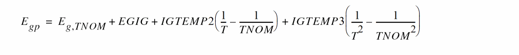
The temperature dependence of the gate current is given by modifying the bandgap specific for the gate current as:
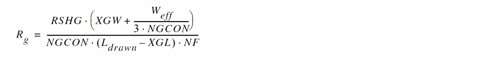
Resistances
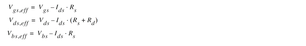
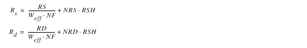
The source and the drain resistances Rs and Rd are considered by voltage drops on each terminal as:
where
The flag CORSRD is provided for the selection of one of the possible approaches.
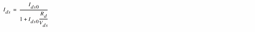
CORSRD = 0 refers to no contact resistance. CORSRD =1, 2, -1 means "internal", "analytical", and "external" source/drain resistances, respectively. CORSRD = 0 is the default. CORSRD=2 is introduced to avoid simulation time penalty with an analytical description of the resistance effect as:
where Ids0 is the drain current without the resistance effect.
Capacitances
Intrinsic Capacitances
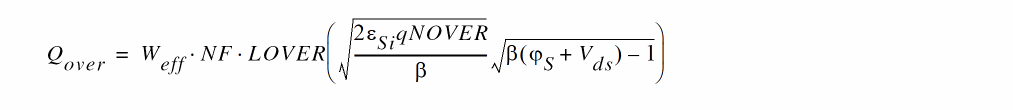
Overlap Capacitances
Surface Potential-Based Model
under the depletion and the accumulation conditions
under inverse condition
Simplified Bias Dependent Model
Extrinsic Capacitances
Leakage Currents
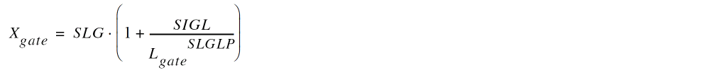
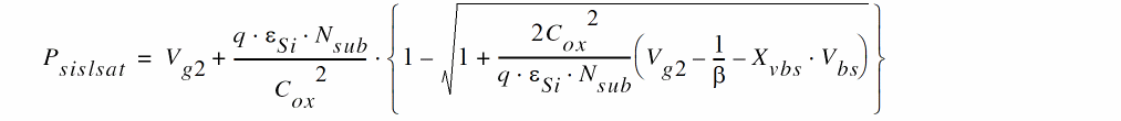
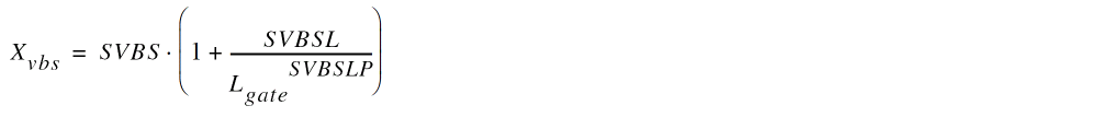
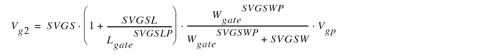
Substrate Current
Impact-Ionization Induced Bulk Potential Change
where
IBPC1 and IBPC2 are model parameters.
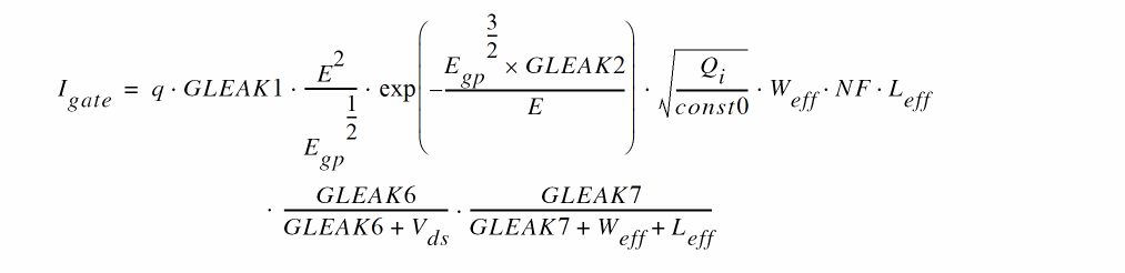
Gate Current
Between Gate and Channel, Igate
where
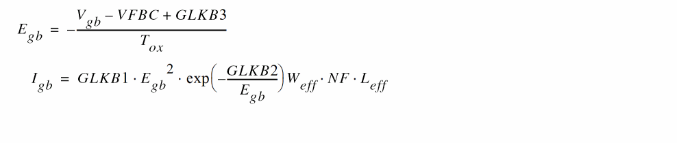
Between Gate and Bulk, Igb
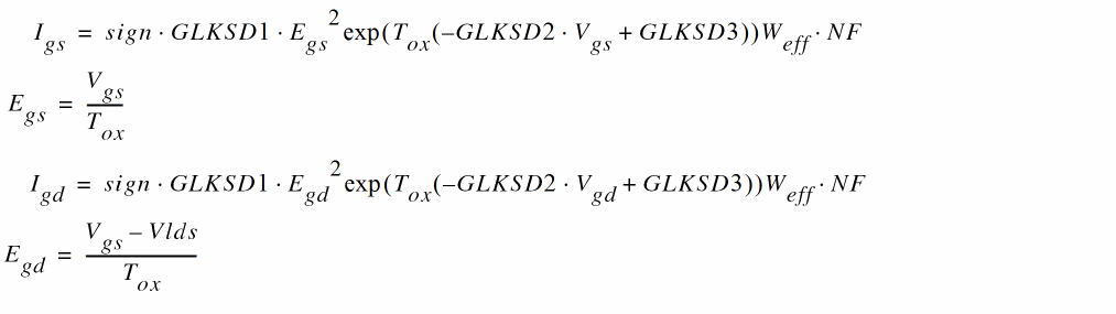
Between Gate and Source/Drain. Igs/Igd
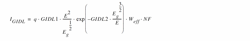
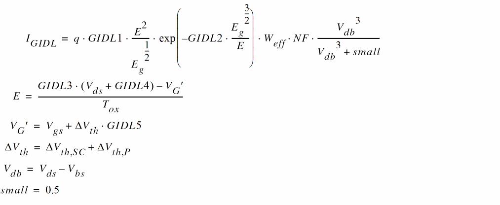
Gate-Induced Drain Leakage (GIDL)
HiSIM 2.5
HiSIM 2.5.1
Conservation of Symmetry at Vds=0
HiSIM preserves the symmetry at Vds = 0 automatically due to the drift-diffusion approximation. However, modeling of the short-channel effects induces a small asymmetry. To eliminate the asymmetry caused by the artifacts of the modeling, the Vth modeling has to include a damping of the short-channel effects as Vds approaches zero. This corresponds to a vanishing of shortchannel effects as Vds gets near to zero, which is also observed in 2D simulations. In HiSIM, the damping is done by a mathematical function with two parameters: VZADD0 and PZADD0.
The values of these parameters are fixed, and it is recommended not to change them. Other modeled phenomena, which include a Vds dependence, cause a similar symmetry problem as the short-channel effects. They are therefore also damped.
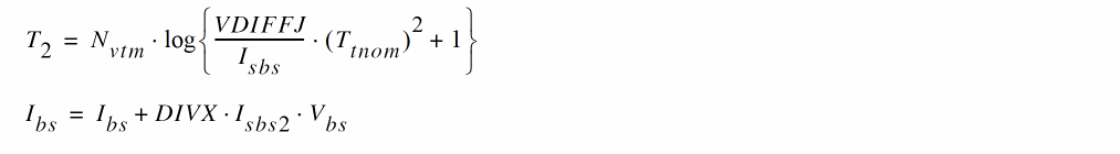
Source/Bulk and Drain/Bulk Diode Model
Diode Current
The model equations for the source/bulk and drain/bulk diode currents are based on the concepts of BSIM3v3, but include a number of modifications.
These regions are distinguished in the modeling and are treated separately according to their origins.
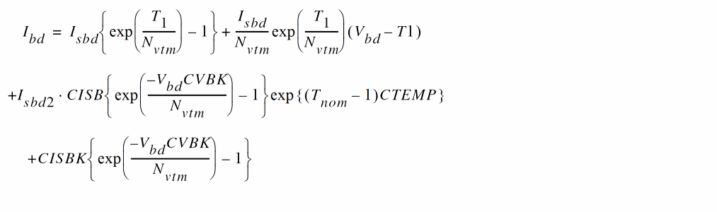
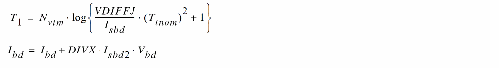
Between Drain and Bulk
With these current densities and the area parameter AD and the perimeter parameter PD of the drain region, the forward and backward currents between drain and bulk are calculated as
a) Vbd >T1
b) T1>Vbd
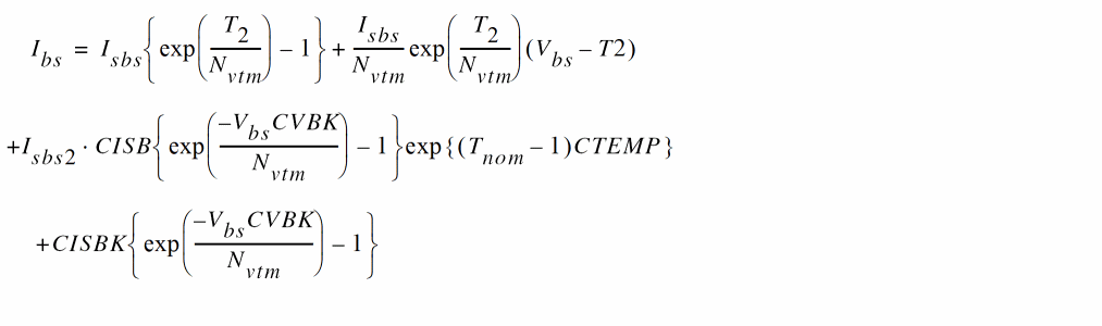
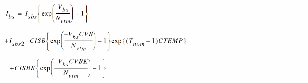
Between Source and Bulk
The area parameter AS and the perimeter parameter PS of the source region are used to calculate the forward and backward currents between source and bulk.
a) Vbs >T2
b) T2>Vbs
Diode Capacitance
The notations
Θ= S; θ= s (for source/bulk junction) and
Θ = D;θ = d (for drain/bulk junction) apply.
P >Weff
>Weff
P <Weff
<Weff
Noise Models
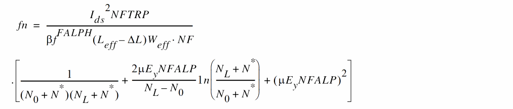
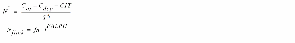
1/f Noise Model
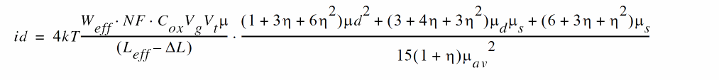
Thermal Noise Model
where  s,
s,  d and
d and  av are mobility at the source side, the drain side, and averaged, respectively.
Shot Noise
HiSIM 2.5
HiSIM 2.5.1
shot noise due to Igs
shot noise due to Igd
shot noise due to Igb
Induced Gate Noise Model
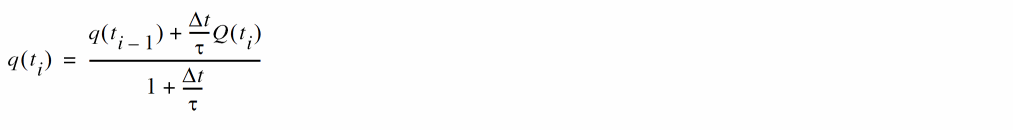
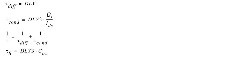
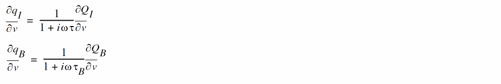
Non-Quasi-Static (NQS) Model
Carrier Formation
Delay Mechanism
Time-Domain Analysis
The total drain/source/bulk terminal currents are derived from the superposition of the transport current and the charging current. The transport current is a function of the instantaneous terminal voltages and is approximated by the steady-state solution. The source/drain/bulk charging currents are the time derivatives of the associated non-quasi-static charges, qS, qD, and qB, respectively.
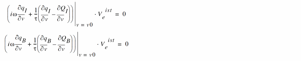
AC Analysis
where
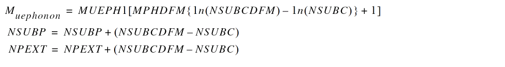
DFM Model
To support design for manufacturability (DFM) HiSIM2 introduces an option for considering the variation of device parameters.
Accurate prediction of device performance for a wide range of the substrate-impurity-concentration variations is secured by introducing an impurity concentration dependent mobility due to the phonon scattering as
where NSUBCDFM is an instance parameter and MPHDFM is a model parameter describing the mobility reduction as the substrate impurity concentration is increased. This model parameter MPHDFM is required, if the model flag CODFM is switched to one. The default value is sufficient for the most applications. The DFM model is activated, if the instance parameter NSUBCDFM is also given.
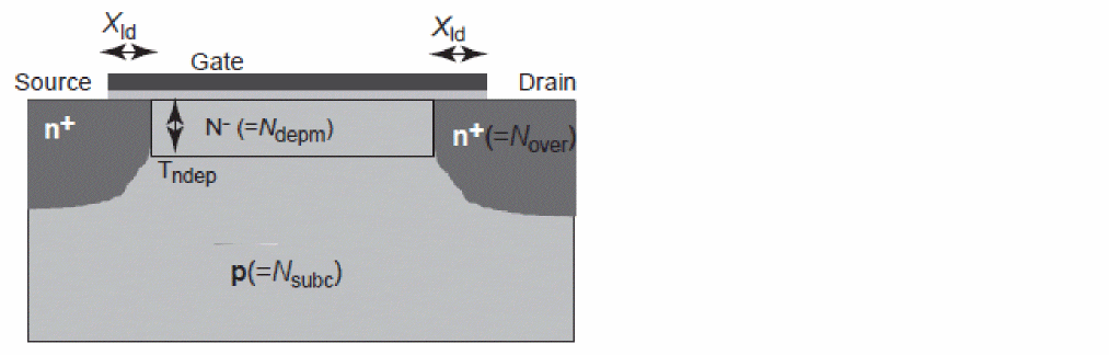
Depletion Mode Model Option
In the depletion model MOSFET, an N- layer is constructed at the channel surface of the conventional MOSFET devices, as shown below.
This model is activated when the parameter CODEP is set to 1.
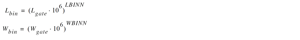
Binning Model
Binning option is introduced in HiSIM2.4 to secure enough accuracy of model calculation results, even though the effects observed are not modeled yet. The binning method is the same as that used in BSIM3/4
where P1, P2, and P3 are model parameters for L HiSIM model parameter, W HiSIM model parameter, and L* HiSIM model parameter, respectively and
Component Statements
This device is supported within altergroups.
Sample Instance Statement
m4 (0 2 1 1) nch w=2u l=0.8u as=250p ad=250p pd=168p ps=168p m=2
Sample Model Statement
model nch hisim2 type=n version=2.50 corsrd=0 conqs=0 cgso=7.43e-10 cgdo=7.43e-10 cgbo=2.56e-11
Instance Definition
Name d g s b ModelName parameter=value ...
Instance Parameters
|
w (m)
|
Gate width.
|
|
l (m)
|
Gate length.
|
|
as (m2)
|
Area of source junction.
|
|
ad (m2)
|
Area of drain junction.
|
|
ps (m)
|
Perimeter of source junction.
|
|
pd (m)
|
Perimeter of drain junction.
|
|
temp (C)
|
Device temperature.
|
|
dtemp (C)
|
Device temperature rise from ambient.
|
|
nrs=0
|
Number of squares of source diffusion. Default value is 1.0 for the 2.50 and 2.51 versions.
|
|
nrd=0
|
Number of squares of drain diffusion. Default value is 1.0 for the 2.50 and 2.51 versions.
|
|
corbnet
|
Substrate resistance network selector.
|
|
rbpb (Ω)
|
Substrate resistance network.
|
|
rbpd (Ω)
|
Substrate resistance network.
|
|
rbps (Ω)
|
Substrate resistance network.
|
|
rbdb (Ω)
|
Substrate resistance network.
|
|
rbsb (Ω)
|
Substrate resistance network.
|
|
corg
|
Gate-contact resistance selector.
|
|
ngcon=1.0
|
Number of gate contacts.
|
|
xgw=0.0 m
|
Distance from gate contact to channel edge.
|
|
xgl=0.0 m
|
Offset of gate length due to variation in patterning.
|
|
nf=1.0
|
Number of gate fingers.
|
|
lod=1.0E-5 m
|
Length of diffusion between gate and STI.
|
|
m=1
|
Multiplicity factor (number of MOSFETs in parallel).
|
|
sa=0.0 m
|
Distance from STI edge to Gate edge, existed from 2.40.
|
|
sb=0.0 m
|
Distance from STI edge to Gate edge, existed from 2.40.
|
|
sd=0.0 m
|
Distance from Gate edge to Gate edge, existed from 2.40.
|
|
nsubcdfm (cm-3)
|
Constant part of Nsub for DFM, existed from 2.40.
|
|
mphdfm
|
NSUBCDFM dependence of phonon scattering for DFM.
|
|
isnoisy=yes
|
Should device generate noise. Possible values are yes and no.
|
|
sca=0.0
|
WPE sca.
|
|
scb=0.0
|
WPE scb.
|
|
scc=0.0
|
WPE scc.
|
|
region=triode
|
Estimated operating region. Possible values are off, triode, sat, subth, and breakdown.
|
|
trise=0 C
|
Default device temperature rise from ambient.
|
Model Definition
model modelName hisim2 parameter=value ...
Model Parameters
Device type parameters
|
type=n
|
Transistor type. Possible values are n and p.
|
|
version=2.50
|
Model parameter "version" accepts only real number values, like 2.50 for version=2.5.0. The available versions are 2.50(2.5.0), 2.51(2.5.1), 2.60(2.6.0), 2.61(2.6.1), 2.70(2.7.0), 2.80(2.8.0), 2.90(2.9.0), 2.91(2.9.1), 3.0(3.0.0), 3.10(3.1.0), 3.11(3.1.1) and 3.20(3.2.0). The parameter cannot be parameterized, its value must be constant.
|
|
corsrd=0
|
Contact resistances Rs and Rd selector.
Possible values are:
0 : no (default).
1 : yes, as internal resistances.
-1 : yes, as external resistances.
|
|
coiprv=1
|
Previous Ids is used for calculating source/drain resistance effect. Possible values are 0 : no and 1 : yes.
|
|
copprv=1
|
Previous surface potential is used for the initial guess. Possible values are 0 : no and 1 : yes.
|
|
coadov=1
|
Selector for lateral field induced and overlap charges/capacitances being added to intrinsic ones. Possible values are 0 : no and 1 : yes(default).
|
|
coisub=0
|
Substrate current selector. Possible values are 0 : no(default) and 1 : yes.
|
|
cogidl=0
|
GIDL current calculation selector. Possible values are 0 : no(default) and 1 : yes.
|
|
coiigs=0
|
Gate current calculation selector. Possible values are 0 : no(default) and 1 : yes.
|
|
coovlp=1
|
Overlap capacitance calculation selector. Possible values are 0 : constant overlap capacitance(default) and 1 : yes.
|
|
coflick=0
|
1/f noise calculation selector.
|
|
coisti=0
|
STI leakage current calculation selector. Possible values are 0 : no(default) and 1 : yes.
|
|
conqs=0
|
Non-quasi-static mode selector. Possible values are 0 : no(default) and 1 : yes.
|
|
cothrml=0
|
Thermal noise calculation selector. Possible values are 0 : no(default) and 1 : yes.
|
|
tnom (C)
|
Parameters measurement temperature. Default set by options.
|
|
corg=0
|
Gate-contact resistance calculation selector. Possible values are 0 : no(default) and 1 : yes.
|
|
corbnet=0
|
Substrate resistance network selector.
|
|
coign=0
|
Induced gate and cross correlation noise calculation selector.
|
|
compatible
|
Compatibility with spice3. Default value is spectre. Possible values are spectre, spice2, spice3, cdsspice, spiceplus, eldo, and sspice.
|
|
alarm=none
|
Forbidden operating region. Possible values are none, off, triode, sat, subth, and rev.
|
|
codfm=0
|
Calculation of model for DFM selector, existed from 2.40.
|
|
corecip=1
|
Capacitance reciprocity takes first priority.
|
|
coqy=0
|
Calculate lateral field-induced charge/capacitance.
|
Safe Operating Areas Parameters
|
vds_max=∞ V
|
Maximum allowed voltage cross source and drain.
|
|
vgd_max=∞ V
|
Maximum allowed voltage cross drain and gate.
|
|
vgs_max=∞ V
|
Maximum allowed voltage cross source/bulk and gate.
|
|
vbd_max=∞ V
|
Maximum allowed voltage cross drain/source and bulk.
|
|
vbs_max=∞ V
|
Maximum allowed voltage cross source and bulk.
|
|
vgb_max=∞ V
|
Maximum allowed voltage cross gate and bulk.
|
|
vgdr_max=vgd_max V
|
Maximum allowed reverse voltage across gate and drain.
|
|
vgsr_max=vgs_max V
|
Maximum allowed reverse voltage across gate and source.
|
|
vgsr_max=vgb_max V
|
Maximum allowed reverse voltage across gate and bulk.
|
|
vgsr_max=vbs_max V
|
Maximum allowed reverse voltage across bulk and source.
|
|
vgsr_max=vbd_max V
|
Maximum allowed reverse voltage across bulk and drain.
|
Default for instance parameters
|
w=5e-6 m
|
Default gate width.
|
|
l=5e-6 m
|
Default gate length.
|
|
as=0 m2
|
Default area of source junction.
|
|
ad=0 m2
|
Default area of drain junction.
|
|
ps=0 m
|
Default perimeter of source junction.
|
|
pd=0 m
|
Default perimeter of drain junction.
|
|
temp=27 C
|
Default device temperature.
|
|
dtemp=0 C
|
Default device temperature rise from ambient.
|
Basic Device Parameters
|
tox=3.0e-9 m
|
Physical oxide thickness.
|
|
xld=0 m
|
Gate-overlap length.
|
|
xwd=0 m
|
Gate-overlap width.
|
|
tpoly=2.0E-7 m
|
Height of the gate poly-si for fringing capacitance.
|
|
nsubc=5.0e+17 cm-3
|
Substrate-impurity concentration.
|
|
nsubp=1.0e+18 cm-3
|
Maximum pocket concentration.
|
|
rs=0.0 Ω m
|
Source contact resistance in LDD region.
|
|
rd=0.0 Ω m
|
Drain contact resistance in LDD region.
|
|
vfbc=-1.0 V
|
Constant part of flat-band voltage.
|
|
lp=1.5e-8 m
|
Length of the pocket penetration into the channel.
|
|
xqy=10e-9 m
|
Distance from channel/drain junction to maximum electric field point.
|
|
lover=5.0E-8 m
|
Overlap length.
|
|
ll=0.0
|
Gate length parameter.
|
|
lld=0.0 m
|
Gate length parameter.
|
|
lln=0.0
|
Gate length parameter.
|
|
wl=0.0
|
Gate width parameter.
|
|
wld=0.0 m
|
Gate width parameter.
|
|
wln=0.0
|
Gate width parameter.
|
|
vbi=1.0 V
|
Built-in potential.
|
|
nsubpw=0.0 cm-3
|
Pocket implant parameter.
|
|
nsubpwp=1.0
|
Pocket implant parameter.
|
|
lpext=1.0E-50 m
|
Pocket extension.
|
|
npext=5.0E17 cm-3
|
Pocket extension.
|
|
rsh=0.0 V/A m
|
Source/drain diffusion sheet resistance.
|
|
rshg=0.0 V/A m
|
Gate-electrode sheet resistance.
|
|
rbpb=50.0 Ω
|
Substrate resistance network.
|
|
rbpd=50.0 Ω
|
Substrate resistance network.
|
|
rbps=50.0 Ω
|
Substrate resistance network.
|
|
rbdb=50.0 Ω
|
Substrate resistance network.
|
|
rbsb=50.0 Ω
|
Substrate resistance network.
|
|
gbmin=1.0E-12
|
Minimum conductance for substrate resistance network.
|
|
xl=0 m
|
Gate length offset due to mask/etch effect, existed from 2.40.
|
|
xw=0 m
|
Gate width offset due to mask/etch effect, existed from 2.40.
|
|
xqy1=0.0 F m^{XQY2}
|
Vbs dependence of Qy, existed from 2.40.
|
|
xqy2=2.0
|
Lgate dependence of Qy, existed from 2.40.
|
|
nsubpl=0.001 μm
|
Gate-length dependence of NSUBP.
|
|
nsubpfac=1.0
|
Gate-length dependence of NSUBP.
|
Temperature dependence effects
|
eg0=1.1785 eV
|
Constant bandgap.
|
|
bgtmp1=9.025e-5 eV/K
|
First order temperature coefficient for band gap.
|
|
bgtmp2=1.0e-7 eV/K2
|
Second order temperature coefficient for band gap.
|
|
copb20compat=1
|
Pb20(compat) or Pb2.
|
|
ctempd=0.0
|
Temperature coefficient for drain junction.
|
|
ctemps=0.0
|
Temperature coefficient for source junction.
|
Quantum Mechanical Effects
|
qme1=0.0 m/V2
|
Coefficient for quantum mechanical effect.
|
|
qme2=0.0 V
|
Coefficient for quantum mechanical effect.
|
|
qme3=0.0 m
|
Coefficient for quantum mechanical effect.
|
|
kappa=3.9
|
Dielectric constant for high-k stacked gate.
|
Poly Depletion Effects
|
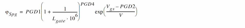
pgd1=1.0E-4 V
|
Strength of poly depletion.
|
|
pgd2=0.3 V
|
Threshold voltage of poly depletion.
|
|
pgd4=0.0
|
Parameter for gate-poly depletion.
|
Short Channel Effects
|
parl2=1.0e-8 m
|
Depletion width of channel/contact junction.
|
|
sc1=1.0 1/V
|
Short-channel coefficient 1.
|
|
sc2=0.0 1/V2
|
Short-channel coefficient 2.
|
|
sc2d=0.0
|
Vds-dependent SCE associated with NSUBD (vertDop).
|
|
sc3=0.0 m/V2
|
Short-channel coefficient 3.
|
|
scp1=1.0 1/V
|
Short-channel coefficient 1 for pocket.
|
|
scp2=0.0 1/V2
|
Short-channel coefficient 2 for pocket.
|
|
scp3=0.0 m/V2
|
Short-channel coefficient 3 for pocket.
|
|
scp22=0.0 V4
|
Short-channel-effect modification for small Vds.
|
|
scp21=0.0 V
|
Short-channel-effect modification for small Vds.
|
|
bs1=0.0 V2
|
Body-coefficient modification by impurity profile.
|
|
bs2=0.9 V
|
Body-coefficient modification by impurity profile.
|
|
sc4=0.0
|
Short-channel coefficient 4.
|
|
copspt=0
|
Flag Ps0 method for deep punchthrough.
|
|
copt=0
|
Flag punchthrough.
|
Narrow channel effects
|
wfc=0.0 m F/cm2
|
Threshold voltage reduction.
|
|
nsti=1.0e17 cm-3
|
Substrate-impurity concentration at the SIT edge.
|
|
wsti=0.0 m
|
Width of the high-field region at STI.
|
|
muephw=0.0
|
Phonon scattering parameter.
|
|
muepwp=1.0
|
Phonon scattering parameter.
|
|
wvth0=0.0
|
Threshold voltage shift.
|
|
mueswp=1.0
|
Change of surface roughness related mobility.
|
|
vthsti=0.0
|
Parameter for STI.
|
|
muesti1=0.0
|
STI Stress mobility parameter.
|
|
muesti2=0.0
|
STI Stress mobility parameter.
|
|
muesti3=1.0
|
STI Stress mobility parameter.
|
|
nsubpsti1=0.0 m
|
STI Stress pocket implant parameter.
|
|
nsubpsti2=0.0 m
|
STI Stress pocket implant parameter.
|
|
nsubpsti3=1.0 m
|
STI Stress pocket implant parameter.
|
|
wstil=0.0
|
Parameter for STI.
|
|
wstilp=1.0
|
Parameter for STI.
|
|
scsti1=0.0
|
Parameter for STI.
|
|
scsti2=0.0 1/V
|
Parameter for STI.
|
|
saref=1e-6 m
|
Reference distance from STI edge to Gate edge, existed from 2.40.
|
|
sbref=1e-6 m
|
Reference distance from STI edge to Gate edge, existed from 2.40.
|
|
wstiw=0.0
|
Parameter for STI, existed from 2.40.
|
|
wstiwp=1.0
|
Parameter for STI, existed from 2.40.
|
|
vdsti=0.0
|
parameter for STI, existed from 2.40.
|
|
nsubcw=0.0
|
Parameter for narrow channel effect.
|
|
nsubcwp=1.0
|
Parameter for narrow channel effect.
|
|
nsubcmax=5e18
|
Parameter for narrow channel effect.
|
Mobility Effects
|
vds0=0.05 V
|
Drain voltage for extracting the low-field mobility.
|
|
muecb0=1000.0 cm2/(V s)
|
Coulomb scattering.
|
|
muecb1=100.0 cm2/(V s)
|
Coulomb scattering.
|
|
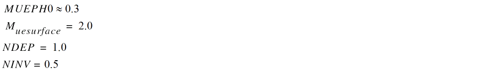
mueph0=0.3 cm2 (V/cm)^(muesr1)/(V s)
|
|
|
Phonon scattering.
|
|
mueph1=2.5e4
|
Phonon scattering.
|
|
muetmp=1.5
|
Temperature dependence of phonon scattering.
|
|
muesr0=2.0 cm2 (V/cm)^(muesr1)/(V s)
|
|
|
Surface-roughness scattering.
|
|
muesr1=1.0e15
|
Surface-roughness scattering.
|
|
ndep=1.0
|
Coefficient of effective electric field.
|
|
ninv=0.5
|
Coefficient of effective electric field.
|
|
bb=2.0
|
High-field mobility degradation.
|
|
vmax=1.0e7 cm/s
|
Maximum of electron saturation velocity.
|
|
vover=0.3 cm^(voverp)
|
Parameter for velocity overshoot.
|
|
voverp=0.3
|
Lgate dependence of velocity overshoot.
|
|
vovers=0.0
|
Parameter for overshoot.
|
|
voversp=0.0
|
Parameter for overshoot.
|
|
vtmp=0.0 cm/s
|
Temperature dependence of the saturation velocity.
|
|
muephl=0.0
|
Phonon scattering parameter.
|
|
mueplp=1.0
|
Phonon scattering parameter.
|
|
muesrl=0.0
|
Surface roughness parameter.
|
|
muesrw=0.0
|
Change of surface roughness related mobility.
|
|
mueslp=1.0
|
Surface roughness parameter.
|
|
ndepl=0.0
|
Modification of Qb contribution for short-channel case, existed from 2.40.
|
|
ndeplp=1.0
|
Modification of Qb contribution for short-channel case, existed from 2.40.
|
|
ninvd=0.0 1/V
|
Modification of Vdse dependence on Eeff.
|
|
muephl2=0.0
|
Length dependence of phonon mobility reduction.
|
|
mueplp2=1.0
|
Length dependence of phonon mobility reduction.
|
Small size parameters
|
wl1=0.0
|
Threshold voltage shift of STI leakage due to small size effect.
|
|
wl1p=1.0
|
Threshold voltage shift of STI leakage due to small size effect.
|
|
wl2=0.0
|
Threshold voltage shift due to small size effect.
|
|
wl2p=1.0
|
Threshold voltage shift due to small size effect.
|
|
muephs=0.0
|
Mobility modification due to small size.
|
|
muepsp=1.0
|
Mobility modification due to small size.
|
|
muepwd=0.0
|
Phonon scattering parameter.
|
|
muepld=0.0
|
Phonon scattering parameter.
|
Channel Length Modulation Effects
|
clm1=0.7
|
First parameter for CLM.
|
|
clm2=2.0 1/m
|
Second parameter for CLM.
|
|
clm3=1.0
|
Third parameter for CLM.
|
|
clm5=1.0
|
Effect of pocket implantation.
|
|
clm6=0.0
|
Effect of pocket implantation.
|
Substrate Current Effects (URC)
|
sub1=10.0 1/V
|
First parameter for Isub.
|
|
sub2=25.0 V
|
Second parameter for Isub.
|
|
svgs=0.8
|
Substrate current dependence on Vgs.
|
|
svbs=0.5
|
Substrate current dependence on Vbs.
|
|
svbsl=0.0
|
Lgate dependence of SVBS.
|
|
svds=0.8
|
Substrate current dependence on Vds.
|
|
slg=3.0E-8
|
Substrate current dependence on Lgate.
|
|
sub1l=2.5E-3
|
Lgate dependence of SUB1.
|
|
sub2l=2.0E-6
|
Lgate dependence of SUB2.
|
|
svgsl=0.0
|
Lgate dependence of SVGS.
|
|
svgslp=1.0
|
Lgate dependence of SVGS.
|
|
svgswp=1.0
|
Wgate dependence of SVGS.
|
|
svgsw=0.0
|
Wgate dependence of SVGS.
|
|
svbslp=1.0
|
Lgate dependence of SVBS.
|
|
slgl=0.0
|
Substrate current dependence on Lgate.
|
|
slglp=1.0
|
Substrate current dependence on Lgate.
|
|
sub1lp=1.0
|
Lgate dependence of SUB1.
|
|
ibpc1=0.0
|
Impact-ionization induced bulk potential change.
|
|
ibpc2=0.0
|
Impact-ionization induced bulk potential change.
|
|
subtmp=0.0
|
Temperature dependence of Isub.
|
Gate Current Effects
|
glpart1=0.5
|
Partitioning of gate current.
|
|
gleak1=50.0 A/(V^(3/2) c^(1/2))
|
|
|
First gate current coefficient.
|
|
gleak2=1.0E7 1/(V^(1/2) c^(3/2) m)
|
|
|
Second gate current coefficient.
|
|
gleak3=6.0E-2
|
Third gate current coefficient.
|
|
gleak4=4.0
|
Parameter for gate current.
|
|
gleak5=7.5E3
|
Parameter for gate current.
|
|
glksd1=1.0E-15
|
Parameter for gate current.
|
|
glksd2=5e-6
|
Parameter for gate current.
|
|
glksd3=-5e-6
|
Parameter for gate current.
|
|
glkb1=5.0E-16
|
Parameter for gate current.
|
|
glkb2=1.0
|
Parameter for gate current.
|
|
igtemp2=0.0
|
Parameter for gate current.
|
|
igtemp3=0.0
|
Parameter for gate current.
|
|
gleak6=0.25 V
|
Parameter for gate current.
|
|
gleak7=1.0E-6 m2
|
Parameter for gate current.
|
|
glkb3=0e0 V
|
Parameter for gate current, existed from 2.40.
|
|
egig=1.1 V
|
Parameter for gate current, existed from 2.40.
|
GIDL Current Effects (URC)
|
gidl1=2.0 A m/(V^(3/2) c^(1/2))
|
|
|
First parameter for GIDL.
|
|
gidl2=3.0E7 1/(V^(1/2) c^(3/2) m)
|
|
|
Second parameter for GIDL.
|
|
gidl3=0.9
|
Third parameter for GIDL.
|
|
gidl4=0.9
|
Parameter for GIDL.
|
|
gidl5=0.2
|
Parameter for GIDL.
|
Noise 1/f Effects
|
nfalp=1.0e-19
|
Flicker (1/f) noise contribution of the mobility fluctuation.
|
|
nfalp1=1.0E-19
|
Contribution of the mobility fluctuation.
|
|
nfalp2=1.0E-19
|
Contribution of the mobility fluctuation.
|
|
sidp=2.0
|
Parameter for 1/f noise.
|
|
dlnoise=0.0
|
Parameter for 1/f noise.
|
|
nftrp=1.0e10
|
Flicker (1/f) noise ratio of trap density to attenuation coefficient.
|
|
cit=0.0
|
Flicker (1/f) noise interface trapped carriers capacitance.
|
|
falph=1.0
|
Parameter for 1/f noise.
|
NQS parameters
|
dly1=1.0E-10
|
Parameter for transit time.
|
|
dly2=0.7
|
Parameter for transit time.
|
|
dly3=8.0E-7 Ω
|
Parameter for transforming bulk charge.
|
Symmetry for Short-Channel MOSFET
|
vzadd0=20.0e-3 V
|
Symmetry conservation coefficient Vzadd at Vds=0.
|
|
pzadd0=20.0e-3 V
|
Symmetry conservation coefficient Pzadd at Vds=0.
|
P-N junctions parameters
|
js0=5.0e-7 A/m2
|
Junction saturation current density.
|
|
js0sw=0.0 A/m
|
Side-wall saturation current density.
|
|
nj=1.0
|
Junction emission coefficient.
|
|
njsw=1.0
|
Junction emission coefficient (sidewall).
|
|
xti=2.0
|
Junction saturation current temperature exponent coefficient.
|
|
cj=5.0e-4 F/m2
|
Bottom junction capacitance per unit area at zero bias.
|
|
cjsw=5e-10 F/m
|
Source/drain sidewall junction capacitance per unit length at zero bias.
|
|
cjswg=5e-10 F/m
|
Source/drain sidewall junction capacitance grading coefficient per unit length at zero bias.
|
|
mj=0.5
|
Bulk junction bottom grading coefficient.
|
|
mjsw=0.33
|
Source/drain sidewall junction capacitance grading coefficient.
|
|
mjswg=0.33
|
Bottom junction capacitance grading coefficient.
|
|
pb=1.0 V
|
Bottom junction build-in potential.
|
|
pbsw=1.0 V
|
Source/drain sidewall junction build-in potential.
|
|
pbswg=1.0 V
|
Source/drain gate sidewall junction build-in potential.
|
|
vdiffj=6.0E-4 V
|
Threshold voltage for S/D junction diode.
|
|
xti2=0.0
|
Temperature coefficient.
|
|
cisb=0.0
|
Reverse bias saturation current.
|
|
cvb=0.0
|
Bias dependence coefficient of cisb.
|
|
ctemp=0.0
|
Temperature coefficient.
|
|
cisbk=0.0 A
|
Reverse bias saturation current.
|
|
cvbk=0.0
|
Bias dependence coefficient of cisb.
|
|
divx=0.0 1/V
|
Parameter for junction.
|
|
tcjbs=0.0
|
Temperature dependence of czbs.
|
|
tcjbd=0.0
|
Temperature dependence of czbd.
|
|
tcjbssw=0.0
|
Temperature dependence of czbssw.
|
|
tcjbdsw=0.0
|
Temperature dependence of czbdsw.
|
|
tcjbsswg=0.0
|
Temperature dependence of czbsswg.
|
|
tcjbdswg=0.0
|
Temperature dependence of czbdswg.
|
|
cisbd=0.0
|
Reverse bias saturation current for drain junction.
|
|
cisbkd=0.0
|
Reverse bias saturation current for drain junction.
|
|
cisbks=0.0
|
Reverse bias saturation current for source junction.
|
|
cisbs=0.0
|
Reverse bias saturation current for source junction.
|
|
cjd=5.0e-4
|
Bottom junction capacitance per unit area at zero bias for drain junction.
|
|
cjs=5.0e-4
|
Bottom junction capacitance per unit area at zero bias for source junction.
|
|
cjswd=5.0e-10
|
Sidewall junction capacitance grading coefficient per unit length at zero bias for drain junction.
|
|
cjswgd=5.0e-10
|
Gate sidewall junction capacitance per unit length at zero bias for drain junction.
|
|
cjswgs=5.0e-10
|
Gate sidewall junction capacitance per unit length at zero bias for source junction.
|
|
cjsws=5.0e-10
|
Sidewall junction capacitance grading coefficient per unit length at zero bias for source junction.
|
|
codio=0
|
Selector for updated diode model
|
|
cvbd=0.0
|
Bias dependence coefficient of cisb for drain junction.
|
|
cvbs=0.0
|
Bias dependence coefficient of cisb for source junction.
|
|
divxd=0.0
|
Reverse coefficient for drain junction.
|
|
divxs=0.0
|
Reverse coefficient for source junction.
|
|
js0d=0.5e-6
|
Saturation current density for drain junction.
|
|
js0s=0.5e-6
|
Saturation current density for source junction.
|
|
js0swd=0.0
|
Side wall saturation current density for drain junction.
|
|
js0swg=0.0
|
Gate sidewall saturation current density.
|
|
js0swgd=0.0
|
Gate side wall saturation current density for drain junction.
|
|
js0swgs=0.0
|
Gate side wall saturation current density for source junction.
|
|
js0sws=0.0
|
Side wall saturation current density for source junction.
|
|
mjd=0.5
|
Bottom junction capacitance grading coefficient for drain junction.
|
|
mjs=0.5
|
Bottom junction capacitance grading coefficient for source junction.
|
|
mjswd=0.33
|
Sidewall junction capacitance grading coefficient for drain junction.
|
|
mjswgd=0.33
|
Gate sidewall junction capacitance grading coefficient for drain junction.
|
|
mjswgs=0.33
|
Gate sidewall junction capacitance grading coefficient for source junction.
|
|
mjsws=0.33
|
Sidewall junction capacitance grading coefficient for source junction.
|
|
njs=1.0
|
Emission coefficient for source junction.
|
|
njswd=1.0
|
Sidewall emission coefficient for drain junction.
|
|
njswg=1.0
|
Gate sidewall emission coefficient.
|
|
njswgd=1.0
|
Gate sidewall emission coefficient for drain junction.
|
|
njswgs=1.0
|
Gate sidewall emission coefficient for source junction.
|
|
njsws=1.0
|
Sidewall emission coefficient for source junction.
|
|
pbd=1.0
|
Bottom junction build-in potential for drain junction.
|
|
pbs=1.0
|
Bottom junction build-in potential for source junction.
|
|
pbswd=1.0
|
Sidewall junction build-in potential for drain junction.
|
|
pbswgd=1.0
|
Gate sidewall junction build-in potential for drain.
|
|
pbswgs=1.0
|
Gate sidewall junction build-in potential for source junction.
|
|
pbsws=1.0
|
Sidewall junction build-in potential for source junction.
|
|
vdiffjd=0.6e-3
|
Threshold voltage for junction diode for drain junction.
|
|
vdiffjs=0.6e-3
|
Threshold voltage for junction diode for source junction.
|
|
xti2d=0.0
|
Temperature coefficient for drain junction.
|
|
xti2s=0.0
|
Temperature coefficient for source junction.
|
|
xtid=2.0
|
Junction current temperature exponent coefficient for drain junction.
|
|
xtis=2.0
|
Junction current temperature exponent coefficient for source junction.
|
Overlap capacitance parameters
|
cgso=0.0 F/m
|
Gate-source overlap capacitance.
|
|
cgdo=0.0 F/m
|
Gate-drain overlap capacitance.
|
|
cgbo=0.0 F/m
|
Gate-bulk overlap capacitance.
|
|
ovslp=2.1E-7
|
Parameter for overlap capacitance.
|
|
ovmag=0.6
|
Parameter for overlap capacitance.
|
|
vfbover=0.0 V
|
Flat-band voltage in overlap region, existed from 2.40.
|
|
nover=1e19 cm-3
|
Impurity concentration in overlap region, existed from 2.40.
|
Smoothing coefficient between linear and saturation
|
ddltmax=10.0
|
Coefficient of effective electric field, existed from 2.40.
|
|
ddltslp=0.0
|
Lgate dependence of smoothing coefficient, existed from 2.40.
|
|
ddltict=10.0
|
Lgate dependence of smoothing coefficient, existed from 2.40.
|
DFM parameters
|
mphdfm=-0.3
|
NSUBCDFM dependence of phonon scattering for DFM, existed from 2.40.
|
Depletion Mode Model Paramrters
|
covdsres=3
|
Vdssatres,Vdsres model switch: (-1) Vdsres=Vds; (3) Vdssatres ln(1+exp) depmos3.
|
|
depcar=0.0
|
Coefficient for Ndrift,res CODEP=3.
|
|
depdvfbc=0.1
|
Delta of Flat-band voltage of the resistor part (CODEP=3).
|
|
depfdpd=0.2
|
Smoothing param for FD/PD transition depmos3.
|
|
deppb0=0.5
|
Flooring for Eeff for Mu_res depmos3.
|
|
depqf=4.0
|
Smoothing param for Vdseff depmos3.
|
|
deprdrdl1=0.0
|
RDRDL1 for resistor layer CODEP=3.
|
|
deprdrdl2=0.0
|
Pinch-off length in resistor layer CODEP=3.
|
|
depmue0=1e3
|
Depletion model parameter.
|
|
depmue0l=0.0
|
Depletion model parameter.
|
|
depmue0lp=1.0
|
Depletion model parameter.
|
|
depmue1=0.0
|
Depletion model parameter.
|
|
depmue1l=0.0
|
Depletion model parameter.
|
|
depmue1lp=1.0
|
Depletion model parameter.
|
|
depmueback0=1e2
|
Depletion model parameter.
|
|
depmueback0l=0.0
|
Depletion model parameter.
|
|
depmueback0lp=1.0
|
Depletion model parameter.
|
|
depmueback1=0.0
|
Depletion model parameter.
|
|
depmueback1l=0.0
|
Depletion model parameter.
|
|
depmueback1lp=1.0
|
Depletion model parameter.
|
|
depmueph0=0.3
|
Depletion model parameter.
|
|
depmueph1=5e3
|
Depletion model parameter.
|
|
depvmax=3e7
|
Depletion model parameter.
|
|
depvmaxl=0.0
|
Depletion model parameter.
|
|
depvmaxlp=1.0
|
Depletion model parameter.
|
|
depvdsef1=2.0
|
Depletion model parameter.
|
|
depvdsef1l=0.0
|
Depletion model parameter.
|
|
depvdsef1lp=1.0
|
Depletion model parameter.
|
|
depvdsef2=0.5
|
Depletion model parameter.
|
|
depvdsef2l=0.0
|
Depletion model parameter.
|
|
depvdsef2lp=1.0
|
Depletion model parameter.
|
|
depbb=1.0
|
Depletion model parameter.
|
|
depmuetmp=1.5
|
Depletion model parameter.
|
WPE: Well Proximity Effects parameters
|
web=0.0
|
Modification of layout characterization factor.
|
|
wec=0.0
|
Modification of layout characterization factor.
|
|
nsubcwpe=0.0 cm-3
|
Channel concentration change due to WPE.
|
|
npextwpe=0.0 cm-3
|
Pocket-tail concentration change due to WPE.
|
|
nsubpwpe=0.0 cm-3
|
Pocket concentration change due to WPE.
|
Binning model parameters which are existed from 2.40
|
lbinn=1.0
|
L modulation coefficient for binning.
|
|
wbinn=1.0
|
W modulation coefficient for binning.
|
|
lvmax=0.0 cm/s
|
Length dependence of vmax.
|
|
lbgtmp1=0.0 eV/K
|
Length dependence of bgtmp1.
|
|
lbgtmp2=0.0 eV/K2
|
Length dependence of bgtmp2.
|
|
leg0=0.0 eV
|
Length dependence of eg0.
|
|
llover=0.0 m
|
Length dependence of lover.
|
|
lvfbover=0.0 V
|
Length dependence of vfbover.
|
|
lnover=0.0 cm-3
|
Length dependence of nover.
|
|
lwl2=0.0
|
Length dependence of wl2.
|
|
lvfbc=0.0 V
|
Length dependence of vfbc.
|
|
lnsubc=0.0 cm-3
|
Length dependence of nsubc.
|
|
lnsubp=0.0 cm-3
|
Length dependence of nsubp.
|
|
lscp1=0.0 1/V
|
Length dependence of scp1.
|
|
lscp2=0.0 1/V2
|
Length dependence of scp2.
|
|
lscp3=0.0 m/V2
|
Length dependence of scp3.
|
|
lsc1=0.0 1/V
|
Length dependence of sc1.
|
|
lsc2=0.0 1/V2
|
Length dependence of sc2.
|
|
lsc3=0.0 m/V2
|
Length dependence of sc3.
|
|
lpgd1=0.0 V
|
Length dependence of pgd1.
|
|
lndep=0.0
|
Length dependence of ndep.
|
|
lninv=0.0
|
Length dependence of ninv.
|
|
lmuecb0=0.0 cm2/(V s)
|
Length dependence of muecb0.
|
|
lmuecb1=0.0 cm2/(V s)
|
Length dependence of muecb1.
|
|
lmueph1=0.0
|
Length dependence of mueph1.
|
|
lvtmp=0.0 cm/s
|
Length dependence of vtmp.
|
|
lwvth0=0.0
|
Length dependence of wvth0.
|
|
lmuesr1=0.0
|
Length dependence of muesr1.
|
|
lmuetmp=0.0
|
Length dependence of muetmp.
|
|
lsub1=0.0 1/V
|
Length dependence of sub1.
|
|
lsub2=0.0 V
|
Length dependence of sub2.
|
|
lsvds=0.0
|
Length dependence of svds.
|
|
lsvbs=0.0
|
Length dependence of svbs.
|
|
lsvgs=0.0
|
Length dependence of svgs.
|
|
lnsti=0.0 cm-3
|
Length dependence of nsti.
|
|
lwsti=0.0 m
|
Length dependence of wsti.
|
|
lscsti1=0.0
|
Length dependence of scsti1.
|
|
lscsti2=0.0 1/V
|
Length dependence of scsti2.
|
|
lvthsti=0.0
|
Length dependence of vthsti.
|
|
lmuesti1=0.0
|
Length dependence of muesti1.
|
|
lmuesti2=0.0
|
Length dependence of muesti2.
|
|
lmuesti3=0.0
|
Length dependence of muesti3.
|
|
lnsubpsti1=0.0 m
|
Length dependence of nsubpsti1.
|
|
lnsubpsti2=0.0 m
|
Length dependence of nsubpsti2.
|
|
lnsubpsti3=0.0 m
|
Length dependence of nsubpsti3.
|
|
lcgso=0.0 F/m
|
Length dependence of cgso.
|
|
lcgdo=0.0 F/m
|
Length dependence of cgdo.
|
|
ljs0=0.0 A/m2
|
Length dependence of js0.
|
|
ljs0sw=0.0 A/m
|
Length dependence of js0sw.
|
|
lnj=0.0
|
Length dependence of nj.
|
|
lcisbk=0.0 A
|
Length dependence of cisbk.
|
|
lclm1=0.0
|
Length dependence of clm1.
|
|
lclm2=0.0 1/m
|
Length dependence of clm2.
|
|
lclm3=0.0
|
Length dependence of clm3.
|
|
lwfc=0.0 m F/cm2
|
Length dependence of wfc.
|
|
lgidl1=0.0 A m/(V^(3/2) c^(1/2))
|
|
|
Length dependence of gidl1.
|
|
lgidl2=0.0 1/(V^(1/2) c^(3/2) m)
|
|
|
Length dependence of gidl2.
|
|
lgleak1=0.0 A/(V^(3/2) c^(1/2))
|
|
|
Length dependence of gleak1.
|
|
lgleak2=0.0 1/(V^(1/2) c^(3/2) m)
|
|
|
Length dependence of gleak2.
|
|
lgleak3=0.0
|
Length dependence of gleak3.
|
|
lgleak6=0.0 V
|
Length dependence of gleak6.
|
|
lglksd1=0.0
|
Length dependence of glksd1.
|
|
lglksd2=0.0
|
Length dependence of glksd2.
|
|
lglkb1=0.0
|
Length dependence of glkb1.
|
|
lglkb2=0.0
|
Length dependence of glkb2.
|
|
lnftrp=0.0
|
Length dependence of nftrp.
|
|
lnfalp=0.0
|
Length dependence of nfalp.
|
|
lvdiffj=0.0 V
|
Length dependence of vdiffj.
|
|
libpc1=0.0
|
Length dependence of ibpc1.
|
|
libpc2=0.0
|
Length dependence of ibpc2.
|
|
lsc4=0.0
|
Length dependence of sc4.
|
|
wvmax=0.0 cm/s
|
Width dependence of vmax.
|
|
wbgtmp1=0.0 eV/K
|
Width dependence of bgtmp1.
|
|
wbgtmp2=0.0 eV/K2
|
Width dependence of bgtmp2.
|
|
weg0=0.0 eV
|
Width dependence of eg0.
|
|
wlover=0.0 m
|
Width dependence of lover.
|
|
wvfbover=0.0 V
|
Width dependence of vfbover.
|
|
wnover=0.0 am-3
|
Width dependence of over.
|
|
wwl2=0.0
|
Width dependence of wl2.
|
|
wvfbc=0.0 V
|
Width dependence of FPC.
|
|
wnsubc=0.0 cm-3
|
Width dependence of nsubc.
|
|
wnsubp=0.0 cm-3
|
Width dependence of nsubp.
|
|
wscp1=0.0 1/V
|
Width dependence of scp1.
|
|
wscp2=0.0 1/V2
|
Width dependence of scp2.
|
|
wscp3=0.0 m/V2
|
Width dependence of scp3.
|
|
wsc1=0.0 1/V
|
Width dependence of sc1.
|
|
wsc2=0.0 1/V2
|
Width dependence of sc2.
|
|
wsc3=0.0 m/V2
|
Width dependence of sc3.
|
|
wpgd1=0.0 V
|
Width dependence of pgd1.
|
|
wndep=0.0
|
Width dependence of ndep.
|
|
wninv=0.0
|
Width dependence of ninv.
|
|
wmuecb0=0.0 cm2/(V s)
|
Width dependence of muecb0.
|
|
wmuecb1=0.0 cm2/(V s)
|
Width dependence of muecb1.
|
|
wmueph1=0.0
|
Width dependence of mueph1.
|
|
wvtmp=0.0 cm/s
|
Width dependence of vtmp.
|
|
wwvth0=0.0
|
Width dependence of wvth0.
|
|
wmuesr1=0.0
|
Width dependence of muesr1.
|
|
wmuetmp=0.0
|
Width dependence of muetmp.
|
|
wsub1=0.0 1/V
|
Width dependence of sub1.
|
|
wsub2=0.0 V
|
Width dependence of sub2.
|
|
wsvds=0.0
|
Width dependence of svds.
|
|
wsvbs=0.0
|
Width dependence of svbs.
|
|
wsvgs=0.0
|
Width dependence of svgs.
|
|
wnsti=0.0 cm-3
|
Width dependence of nsti.
|
|
wwsti=0.0 m
|
Width dependence of wsti.
|
|
wscsti1=0.0
|
Width dependence of scsti1.
|
|
wscsti2=0.0 1/V
|
Width dependence of scsti2.
|
|
wvthsti=0.0
|
Width dependence of vthsti.
|
|
wmuesti1=0.0
|
Width dependence of muesti1.
|
|
wmuesti2=0.0
|
Width dependence of muesti2.
|
|
wmuesti3=0.0
|
Width dependence of muesti3.
|
|
wnsubpsti1=0.0 m
|
Width dependence of nsubpsti1.
|
|
wnsubpsti2=0.0 m
|
Width dependence of nsubpsti2.
|
|
wnsubpsti3=0.0 m
|
Width dependence of nsubpsti3.
|
|
wcgso=0.0 F/m
|
Width dependence of cgso.
|
|
wcgdo=0.0 F/m
|
Width dependence of cgdo.
|
|
wjs0=0.0 A/m2
|
Width dependence of js0.
|
|
wjs0sw=0.0 A/m
|
Width dependence of js0sw.
|
|
wnj=0.0
|
Width dependence of nj.
|
|
wcisbk=0.0 A
|
Width dependence of cisbk.
|
|
wclm1=0.0
|
Width dependence of clm1.
|
|
wclm2=0.0 1/m
|
Width dependence of clm2.
|
|
wclm3=0.0
|
Width dependence of clm3.
|
|
wwfc=0.0 m F/cm2
|
Width dependence of wfc.
|
|
wgidl1=0.0 A m/(V^(3/2) c^(1/2))
|
|
|
Width dependence of gidl1.
|
|
wgidl2=0.0 1/(V^(1/2) c^(3/2) m)
|
|
|
Width dependence of gidl2.
|
|
wgleak1=0.0 A/(V^(3/2) c^(1/2))
|
|
|
Width dependence of gleak1.
|
|
wgleak2=0.0 1/(V^(1/2) c^(3/2) m)
|
|
|
Width dependence of gleak2.
|
|
wgleak3=0.0
|
Width dependence of gleak3.
|
|
wgleak6=0.0 V
|
Width dependence of gleak6.
|
|
wglksd1=0.0
|
Width dependence of glksd1.
|
|
wglksd2=0.0
|
Width dependence of glksd2.
|
|
wglkb1=0.0
|
Width dependence of glkb1.
|
|
wglkb2=0.0
|
Width dependence of glkb2.
|
|
wnftrp=0.0
|
Width dependence of nftrp.
|
|
wnfalp=0.0
|
Width dependence of nfalp.
|
|
wvdiffj=0.0 V
|
Width dependence of vdiffj.
|
|
wibpc1=0.0
|
Width dependence of ibpc1.
|
|
wibpc2=0.0
|
Width dependence of ibpc2.
|
|
wsc4=0.0
|
Width dependence of sc4.
|
|
pvmax=0.0 cm/s
|
Cross-term dependence of vmax.
|
|
pbgtmp1=0.0 eV/K
|
Cross-term dependence of bgtmp1.
|
|
pbgtmp2=0.0 eV/K2
|
Cross-term dependence of bgtmp2.
|
|
peg0=0.0 eV
|
Cross-term dependence of eg0.
|
|
plover=0.0 m
|
Cross-term dependence of lover.
|
|
pvfbover=0.0 V
|
Cross-term dependence of vfbover.
|
|
pnover=0.0 cm-3
|
Cross-term dependence of nover.
|
|
pwl2=0.0
|
Cross-term dependence of wl2.
|
|
pvfbc=0.0 V
|
Cross-term dependence of vfbc.
|
|
pnsubc=0.0 cm-3
|
Cross-term dependence of nsubc.
|
|
pnsubp=0.0 cm-3
|
Cross-term dependence of nsubp.
|
|
pscp1=0.0 1/V
|
Cross-term dependence of scp1.
|
|
pscp2=0.0 1/V2
|
Cross-term dependence of scp2.
|
|
pscp3=0.0 m/V2
|
Cross-term dependence of scp3.
|
|
psc1=0.0 1/V
|
Cross-term dependence of sc1.
|
|
psc2=0.0 1/V2
|
Cross-term dependence of sc2.
|
|
psc3=0.0 m/V2
|
Cross-term dependence of sc3.
|
|
ppgd1=0.0 V
|
Cross-term dependence of pgd1.
|
|
pndep=0.0
|
Cross-term dependence of ndep.
|
|
pninv=0.0
|
Cross-term dependence of ninv.
|
|
pmuecb0=0.0 cm2/(V s)
|
Cross-term dependence of muecb0.
|
|
pmuecb1=0.0 cm2/(V s)
|
Cross-term dependence of muecb1.
|
|
pmueph1=0.0
|
Cross-term dependence of mueph1.
|
|
pvtmp=0.0 cm/s
|
Cross-term dependence of vtmp.
|
|
pwvth0=0.0
|
Cross-term dependence of wvth0.
|
|
pmuesr1=0.0
|
Cross-term dependence of muesr1.
|
|
pmuetmp=0.0
|
Cross-term dependence of muetmp.
|
|
psub1=0.0 1/V
|
Cross-term dependence of sub1.
|
|
psub2=0.0 V
|
Cross-term dependence of sub2.
|
|
psvds=0.0
|
Cross-term dependence of svds.
|
|
psvbs=0.0
|
Cross-term dependence of svbs.
|
|
psvgs=0.0
|
Cross-term dependence of svgs.
|
|
pnsti=0.0 cm-3
|
Cross-term dependence of nsti.
|
|
pwsti=0.0 m
|
Cross-term dependence of wsti.
|
|
pscsti1=0.0
|
Cross-term dependence of scsti1.
|
|
pscsti2=0.0 1/V
|
Cross-term dependence of scsti2.
|
|
pvthsti=0.0
|
Cross-term dependence of vthsti.
|
|
pmuesti1=0.0
|
Cross-term dependence of muesti1.
|
|
pmuesti2=0.0
|
Cross-term dependence of muesti2.
|
|
pmuesti3=0.0
|
Cross-term dependence of muesti3.
|
|
pnsubpsti1=0.0 m
|
Cross-term dependence of nsubpsti1.
|
|
pnsubpsti2=0.0 m
|
Cross-term dependence of nsubpsti2.
|
|
pnsubpsti3=0.0 m
|
Cross-term dependence of nsubpsti3.
|
|
pcgso=0.0 F/m
|
Cross-term dependence of cgso.
|
|
pcgdo=0.0 F/m
|
Cross-term dependence of cgdo.
|
|
pjs0=0.0 A/m2
|
Cross-term dependence of js0.
|
|
pjs0sw=0.0 A/m
|
Cross-term dependence of js0sw.
|
|
pnj=0.0
|
Cross-term dependence of nj.
|
|
pcisbk=0.0 A
|
Cross-term dependence of cisbk.
|
|
pclm1=0.0
|
Cross-term dependence of clm1.
|
|
pclm2=0.0 1/m
|
Cross-term dependence of clm2.
|
|
pclm3=0.0
|
Cross-term dependence of clm3.
|
|
pwfc=0.0 m F/cm2
|
Cross-term dependence of wfc.
|
|
pgidl1=0.0 A m/(V^(3/2) c^(1/2))
|
|
|
Cross-term dependence of gidl1.
|
|
pgidl2=0.0 1/(V^(1/2) c^(3/2) m)
|
|
|
Cross-term dependence of gidl2.
|
|
pgleak1=0.0 A/(V^(3/2) c^(1/2))
|
|
|
Cross-term dependence of gleak1.
|
|
pgleak2=0.0 1/(V^(1/2) c^(3/2) m)
|
|
|
Cross-term dependence of gleak2.
|
|
pgleak3=0.0
|
Cross-term dependence of gleak3.
|
|
pgleak6=0.0 V
|
Cross-term dependence of gleak6.
|
|
pglksd1=0.0
|
Cross-term dependence of glksd1.
|
|
pglksd2=0.0
|
Cross-term dependence of glksd2.
|
|
pglkb1=0.0
|
Cross-term dependence of glkb1.
|
|
pglkb2=0.0
|
Cross-term dependence of glkb2.
|
|
pnftrp=0.0
|
Cross-term dependence of nftrp.
|
|
pnfalp=0.0
|
Cross-term dependence of nfalp.
|
|
pvdiffj=0.0 V
|
Cross-term dependence of vdiffj.
|
|
pibpc1=0.0
|
Cross-term dependence of ibpc1.
|
|
pibpc2=0.0
|
Cross-term dependence of ibpc2.
|
|
psc4=0.0
|
Cross-term dependence of sc4.
|
|
vgsmin=-5 type V
|
Minimal/maximal expected Vgs (NMOS/PMOS).
|
|
sc3vbs=0.0 V
|
Vbs value for clamping sc3.
|
|
muecb0lp=0.0
|
L dependence of MUECB0.
|
|
muecb1lp=0.0
|
L dependence of MUECB1.
|
|
coqovsm=1
|
Select smoothing method of Qover.
|
|
codep=0
|
Selector for depletion device.
|
|
ndepm=1e17
|
N- layer concentration of the depletion MOS model.
|
|
tndep=0.2e-6
|
N- layer depth of the depletion MOS model.
|
|
depleak=0.5
|
Leakage current modification parameter for the depletion MOS model.
|
|
depeta=0.0
|
Vds dependence of threshold voltage for the depletion MOS model.
|
|
coddlt=0
|
Flag used to evaluate DDLT, thus Vdseff. Since version 2.8.0.
|
|
ninvdl=0.0
|
LG dependence of NINVD.
|
|
ninvdlp=1.0
|
LG dependence of NINVD.
|
|
depleakl=0.0
|
L dependence of DEPLEAK.
|
|
depleaklp=1.0
|
L dependence of DEPLEAK.
|
|
ndepml=0.0
|
L dependence of NDEPM.
|
|
ndepmlp=1.0
|
L dependence of NDEPM.
|
|
ndepw=0.0
|
Coefficient of Qbm for Eeff.
|
|
ndepwp=1.0
|
Coefficient of Qbm for Eeff.
|
|
npextw=0.0
|
Modification of extension concentration for narrow width
|
|
npextwp=0.0
|
Modification of extension concentration for narrow width
|
|
lnsubcsti1=0.0 m
|
Length dependence of nsubcsti1.
|
|
lnsubcsti2=0.0 m
|
Length dependence of nsubcsti2.
|
|
lnsubcsti3=0.0 m
|
Length dependence of nsubcsti3.
|
|
wnsubcsti1=0.0 m
|
Wength dependence of nsubcsti1.
|
|
wnsubcsti2=0.0 m
|
Wength dependence of nsubcsti2.
|
|
wnsubcsti3=0.0 m
|
Wength dependence of nsubcsti3.
|
|
pnsubcsti1=0.0 m
|
Cross-term dependence of nsubcsti1.
|
|
pnsubcsti2=0.0 m
|
Cross-term dependence of nsubcsti2.
|
|
pnsubcsti3=0.0 m
|
Cross-term dependence of nsubcsti3.
|
|
lcisbkd=0.0
|
Length dependence of cisbkd.
|
|
lcisbks=0.0
|
Length dependence of cisbks.
|
|
ljs0d=0.0
|
Length dependence of js0d.
|
|
ljs0s=0.0
|
Length dependence of js0s.
|
|
ljs0swd=0.0
|
Length dependence of js0swd.
|
|
ljs0swg=0.0
|
Length dependence of js0swg.
|
|
ljs0sws=0.0
|
Length dependence of js0sws.
|
|
lnjd=0.0
|
Length dependence of njd.
|
|
lnjs=0.0
|
Length dependence of njs.
|
|
lvdiffjd=0.0
|
Length dependence of vdiffjd.
|
|
lvdiffjs=0.0
|
Length dependence of vdiffjs.
|
|
pcisbkd=0.0
|
Cross-term dependence of cisbkd.
|
|
pcisbks=0.0
|
Cross-term dependence of cisbks.
|
|
pjs0d=0.0
|
Cross-term dependence of js0d.
|
|
pjs0s=0.0
|
Cross-term dependence of js0s.
|
|
pjs0swd=0.0
|
Cross-term dependence of js0swd.
|
|
pjs0swg=0.0
|
Cross-term dependence of js0wg.
|
|
pjs0sws=0.0
|
Cross-term dependence of js0sws.
|
|
pnjd=0.0
|
Cross-term dependence of njd.
|
|
pnjs=0.0
|
Cross-term dependence of njs.
|
|
pvdiffjd=0.0
|
Cross-term dependence of vdiffjd.
|
|
pvdiffjs=0.0
|
Cross-term dependence of vdiffjs.
|
|
wcisbkd=0.0
|
Width dependence of cisbkd.
|
|
wcisbks=0.0
|
Width dependence of cisbks.
|
|
wjs0d=0.0
|
Width dependence of js0d.
|
|
wjs0s=0.0
|
Width dependence of js0s.
|
|
wjs0swd=0.0
|
Width dependence of js0swd.
|
|
wjs0swg=0.0
|
Width dependence of js0swg.
|
|
wjs0sws=0.0
|
Width dependence of js0sws.
|
|
wnjd=0.0
|
Width dependence of njd.
|
|
wnjs=0.0
|
Width dependence of njs.
|
|
wvdiffjd=0.0
|
Width dependence of vdiffjd.
|
|
wvdiffjs=0.0
|
Width dependence of vdiffjs.
|
Auto Model Selector parameters
|
wmax=1 m
|
Maximum channel width for which the model is valid.
|
|
wmin=0 m
|
Minimum channel width for which the model is valid.
|
|
lmax=1 m
|
Maximum channel length for which the model is valid.
|
|
lmin=0 m
|
Minimum channel length for which the model is valid.
|
|
nsubcsti1=0.0 m
|
STI Stress Parameter for Nsubc [-].
|
|
nsubcsti2=0.0 m
|
STI Stress Parameter for Nsubc [-].
|
|
nsubcsti3=1.0 m
|
STI Stress Parameter for Nsubc [-].
|
|
gidl6=0
|
Parameter for GIDL [-].
|
|
gidl7=1
|
Parameter for GIDL [-].
|
|
coerrrep=1
|
Selector for error report.
|
|
cofixcss=0
|
Selector for Css problem.
|
|
info=0
|
Print information.
|
|
nsubpdlt=0.01
|
Delta for nsubp smoothing [-].
|
|
vfbcl=0.0
|
Gate-length dependence of VFBC [um].
|
|
vfbclp=1.0
|
Gate-length dependence of VFBC [-].
|
|
depddlt=3.0
|
Smoothing coefficient for Vds, res.
|
|
depmue0tmp=0.0
|
Temperature dependence of DEPmue0.
|
|
depmue2=1E3
|
Coulomb scattering of the resistor part.
|
|
depmue2tmp=0.0
|
Temperature dependence of DEPmue2.
|
|
depmuea1=0.0
|
Modification of mures.
|
|
depninvd=0
|
NINVD for Mu_res depmos3.
|
|
depninvdc=0
|
Modification of Vdse dependence on Eeff (for Mu_res) (CODEP=3).
|
|
depninvdh=0
|
Modification of Vdse dependence on Eeff (for Mu_res) (CODEP=3).
|
|
depninvdl=0
|
NINVDL for Mu_res depmos3.
|
|
depninvdlp=1.0
|
NINVDLP for Mu_res depmos3.
|
|
depninvdw=0.0
|
Coefficient of modification of Vdse dependence on Eeff; Mu_res (CODEP=3).
|
|
depninvdwp=1.0
|
Coefficient of modification of Vdse dependence on Eeff; Mu_res (CODEP=3).
|
|
deprbr=1
|
Parameter for resistance effect along substrate (for minority carrier).
|
|
depps=0.05
|
Ps_delta for smoothing charge depmos3.
|
|
depsubsl=2.0
|
Factor of the sub-threshold slope.
|
|
depsubsl0=2.0
|
Factor of the sub-threshold slope (CODEP=2,3).
|
|
depvfbc=0.2
|
Flat-band voltage of the resistor part.
|
|
depvgpsl=0.0
|
Smoothing coefficient for gm.
|
|
depvsata=0.0
|
Vdssat shift depmos3.
|
|
depvsatr=0.0
|
Vbs dependence of subVds,sat of the resistor part.
|
|
depvtmp=0.0
|
Temperature dependence of DEPVMAX.
|
|
gdl=0.0
|
Strength of high-field effect.
|
|
gdld=0.0
|
Channel-length dependence of high-field effect.
|
|
gdlp=0.0
|
Channel-length dependence of high-field effect.
|
|
gmin=0.0
|
Minimum conductance.
|
|
muephw2=0.0
|
Phonon related mobility reduction.
|
|
muepwp2=1.0
|
Phonon related mobility reduction.
|
|
mupt=0.0
|
Mobility for deep punchthrough.
|
|
njd=1.0
|
Emission coefficient for drain junction.
|
|
njunc=1e20
|
Junction doping conc; deep punchthrough.
|
|
nsubcw2=0.0
|
Modification of substrate concentration for narrow width.
|
|
nsubcwp2=1.0
|
Modification of substrate concentration for narrow width.
|
|
nsubd=5e17
|
Substrate conc for Vbs effects of dVth; 0.0 (deactivate this effects).
|
|
nsubdnw=0.0
|
Substrate conc for Vbs effects of dVth; narrow W effects (vertDop).
|
|
nsubdw=0.0
|
NSUBD W-dependence coefficient. (vertDop).
|
|
nsubdw0=5e17
|
NSUBD W-dependence constant term (vertDop).
|
|
nsubdwp=1
|
NSUBD W-dependence exponent (vertDop).
|
|
ovinvdlt=75.00
|
Analytical overlap inversion when COQOVSM=2.
|
|
pslimpt=0.0
|
Ps0 limit for deep punchthrough.
|
|
pt2=0.0
|
Vds dependence of punchthrough effect.
|
|
pt4=0.0
|
Vbs dependence of punchthrough effect.
|
|
pt4p=1.0
|
Vbs dependence of punchthrough effect.
|
|
ptl=0.0
|
Strength of punchthrough effect.
|
|
ptlp=1.0
|
Channel-length dependence of punchthrough effect.
|
|
ptp=3.5
|
Strength of punchthrough effect.
|
|
qyrat=0.5
|
Partitioning ratio of Qy between source and drain.
|
|
rmin=1E-4
|
Minimum resistance for RS / RD.
|
|
toxov=3E-9
|
Oxide thickness of overlap region.
|
|
vbdr_max=vbd_max V
|
Maximum allowed reverse voltage across bulk and drain.
|
|
vbsr_max=vbs_max V
|
Maximum allowed reverse voltage across bulk and source.
|
|
vbsrfar=(-30.0)
|
Reversely biasing Vb[s|d] farthest from 0 (negatively large;nMOS)(positively large; pMOS).
|
|
vfbpt=0.0
|
dVfb for deep punchthrough.
|
|
vgbr_max=vgb_max V
|
Maximum allowed reverse voltage across gate and bulk.
|
|
vsftd=0
|
Shift Vth vs sqrt(2/phi-Vbs) line for substrate.
|
|
xjpt=3E-8
|
Junction depth; deep punchthrough.
|
|
xldc=0.0
|
Lateral diffusion of S/D under the gate (capacitance).
|
|
wdepv=10.0
|
Cross point of dVthVertdnw and dVthVertd lines (vertDop).
|
|
xwdc=0.0
|
Lateral diffusion along the width dir. (capacitance).
|
Output Parameters
|
tempeff (C)
|
Effective temperature for a single device.
|
|
meff
|
Effective multiplicity factor (m-factor).
|
|
weff (m)
|
Effective channel width.
|
|
leff (m)
|
Effective channel length.
|
|
rseff (Ω)
|
Effective source resistance.
|
|
rdeff (Ω)
|
Effective drain resistance.
|
Operating-Point Parameters
|
reversed
|
Reverse mode indicator. Possible values are yes and no.
|
|
ids (A)
|
Resistive drain-to-source current.
|
|
vgs (V)
|
Gate-source voltage.
|
|
vds (V)
|
Drain-source voltage.
|
|
vbs (V)
|
Bulk-source voltage.
|
|
vth (V)
|
Threshold voltage.
|
|
vdsat (V)
|
Drain-source saturation voltage.
|
|
region=triode
|
Estimated operating region. Possible values are off, triode, sat, subth, and breakdown.
|
|
gm (S)
|
Common-source transconductance.
|
|
gds (S)
|
Common-source output conductance.
|
|
gmbs (S)
|
Body-transconductance.
|
|
qb (Coul)
|
Total bulk charge.
|
|
qd (Coul)
|
Total drain charge.
|
|
qg (Coul)
|
Total gate charge.
|
|
qs (Coul)
|
Total source charge.
|
|
cjd (F)
|
Drain-bulk junction capacitance.
|
|
cjs (F)
|
Source-bulk junction capacitance.
|
|
cgg (F)
|
dQg_dVg.
|
|
cgd (F)
|
dQg_dVd.
|
|
cgs (F)
|
dQg_dVs.
|
|
cgb (F)
|
dQg_dVb.
|
|
cdg (F)
|
dQd_dVg.
|
|
cdd (F)
|
dQd_dVd.
|
|
cds (F)
|
dQd_dVs.
|
|
cdb (F)
|
dQd_dVb.
|
|
csg (F)
|
dQs_dVg.
|
|
csd (F)
|
dQs_dVd.
|
|
css (F)
|
dQs_dVs.
|
|
csb (F)
|
dQs_dVb.
|
|
cbg (F)
|
dQb_dVg.
|
|
cbd (F)
|
dQb_dVd.
|
|
cbs (F)
|
dQb_dVs.
|
|
cbb (F)
|
dQb_dVb.
|
|
id (A)
|
Resistive drain current.
|
|
ig (A)
|
Gate current.
|
|
is (A)
|
Resistive source current.
|
|
ibulk (A)
|
Resistive bulk current.
|
|
pwr (W)
|
Power at operating point.
|
|
ps0 (V)
|
Surface potential at source side.
|
|
psl (V)
|
Surface potential at drain side.
|
|
pds (V)
|
Delta surface potential between psl and ps0.
|
|
isub (A)
|
Substrate current Isub.
|
|
gbds (S)
|
Substrate trans conductance (dIsub/dVds).
|
|
gbgs (S)
|
Substrate trans conductance (dIsub/dVgs).
|
|
gbbs (S)
|
Substrate transconductance (dIsub/dVbs).
|
|
igate (A)
|
Gate current due to tunneling.
|
|
igates (A)
|
Tunneling current from gate to source.
|
|
igateb (A)
|
Tunneling current from gate to bulk.
|
|
igated (A)
|
Tunneling current from gate to drain.
|
|
igisl (A)
|
Gate-induced source leakage current.
|
|
igidl (A)
|
Gate-induced drain leakage current.
|
|
ibs (A)
|
Source-bulk diode current.
|
|
ibd (A)
|
Source-drain diode current.
|
|
cgso (F)
|
Gate-source overlap capacitance.
|
|
cgbo (F)
|
Gate-bulk overlap capacitance.
|
|
cgdo (F)
|
Gate-drain overlap capacitance.
|
Return to top