Reference
Model Equations
Some important model equations are listed as following for your reference:
Charge
All device characteristics are determined on the basis of the charge controlled by applied voltages and by expressing the MOSFET charges as functions of the surface potentials. Under the charge-sheet approximation the charges on the four MOSFET terminals QG(gate), QB(bulk), QD(drain), and QS(source), are described for the symmetrical the source/drain contacts as:
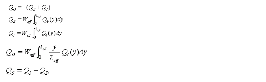
where QB and QI are the depletion charge and the inversion charge, respectively, and y is the position along the channel. Leff and 0 are the channel-end positions at the drain side and the source side, respectively.
Drain Current
The drift-diffusion theory describes the drain current Ids as:
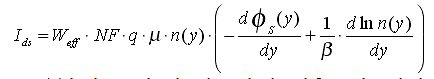
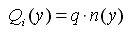
where n(y) is the carrier density calculated from the relationship
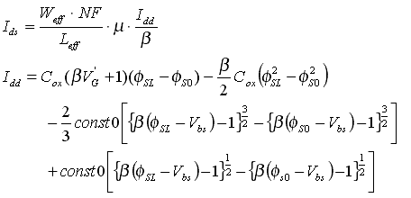
Under the gradual-channel approximation with further approximations of an idealized gate structure and uniform channel doping, the final equation for Ids is written:
Threshold Voltage Shift
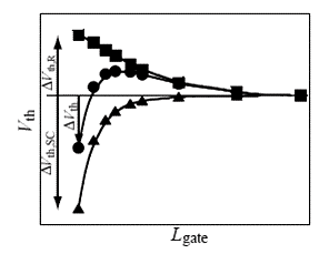
Different from the conventional bsim model, all HiSIM_HV can be determined by oxide thickness Tox and the substrate doping concentration NSUBC. The measured Vth is influenced by various phenomena such as the short-channel effects, which cause a reduction of Vth for short-channel transistors in comparison to long-channel transistors as shown in Figure 31-5. This so-called Vth roll-off is dependent on the technology applied for MOSFET fabrication. Therefore, HiSIM can derive many detailed information on the MOSFET fabrication technology, which are relevant for modeling device characteristics, from the Vth changes (![]() Vth) as a function of gate length (Lgate). The modeled Vth is incorporated in the
Vth) as a function of gate length (Lgate). The modeled Vth is incorporated in the ![]() S iteration can be viewed as consisting of two main effects or components:
S iteration can be viewed as consisting of two main effects or components:
(I) the short-channel effect: ![]() Vth, SC
Vth, SC
(II) the reverse-short-channel effect: ![]() Vth, R and
Vth, R and ![]() Vth, P
Vth, P
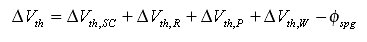
The separation into these two components (![]() Vth =
Vth = ![]() Vth, SC +
Vth, SC + ![]() Vth, R (or
Vth, R (or ![]() Vth, P)) is schematically shown in Figure 31-5.
Vth, P)) is schematically shown in Figure 31-5.
Figure -5 Schematic plot of the separation of Vth into the contributions of the short-channel and the reverse short-channel effect.
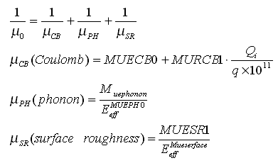
Mobility Model
The low-field mobility is described with the following expressions and includes the three independent mechanisms of Coulomb, phonon and surface-roughness scattering:
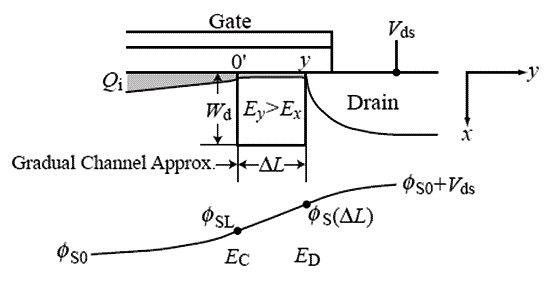
Channel-Length Modulation
As the gradual-channel approximation is not valid for large Vds causing the pinch-off phenomenon in the channel. Without taking into account the pinch-off phenomenon, the calculated channel conductance gds enters abruptly into the saturation condition. To include the pinch-off phenomenon in HiSIM, we apply the conventional method of modeling the pinch-off region (![]() L) separately from the rest of the channel as depicted in Figure 31-6:
L) separately from the rest of the channel as depicted in Figure 31-6:
Figure -6 Schematic showing the correlation among physical quantities in the pinch-off region.
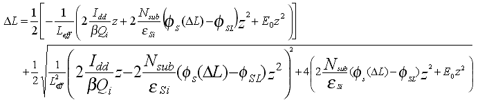
After taking into all effects, the final ![]() L is derived as:
L is derived as:
Narrow-Channel Effects
The shallow-trench-isolation (STI) technology induces a Vth reduction for reduced channel width (Wgate). This phenomenon is modeled under inclusion of the edge-fringing capacitances Cef at the edge of the trench as:
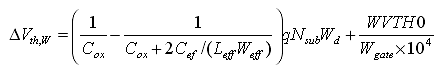
So the total threshold shift becomes:
In addition, the mobility should be adjusted with small geometrical size. The shallow trench isolation induces also an undesired hump in the sub-threshold region of the Ids-Vgs characteristics.
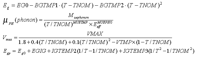
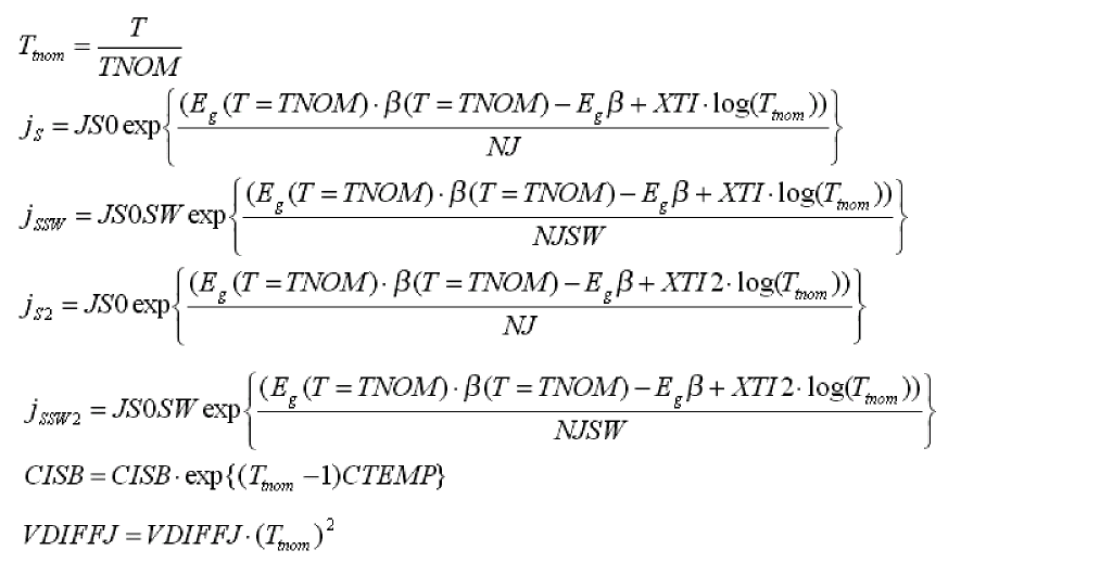
Temperature Dependences
The temperature dependence is included automatically in the surface potentials through ![]() , which is the inverse of the thermal voltage. Additionally the band gap, the intrinsic carrier concentration, the carrier mobility, and the carrier saturation velocity are also temperature dependent.
, which is the inverse of the thermal voltage. Additionally the band gap, the intrinsic carrier concentration, the carrier mobility, and the carrier saturation velocity are also temperature dependent.
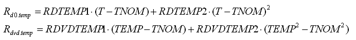
Resistances
Junction Capacitance at Drain side
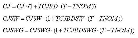
Junction Capacitance at Drain side
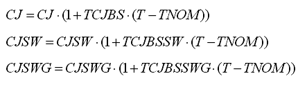
Junction Current
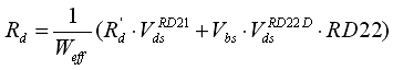
Resistance
For the symmetrical/asymmetrical HVMOS case, the resistance at the source side is modeled with the same equations for the drain side without the Vds dependence. The source and the drain resistances Rs and Rd are considered by voltage drops on each terminal as
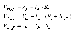
for the DC condition, where the effective voltages are referred as internal node potentials. The resistance values are modeled as
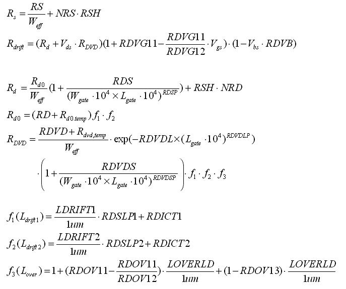
Different resistance effects modeling approaches are supplies by HiSIM_HV model, it can be treated as external resistance or the total current can be obtained by a simple analytical description. Flag CORSRD is provided for the selection of one of the possible approaches. In the HiSIM HV 1.1.1 version the resistances is treated only as the extrinsic resistances.
CORSRD=2 is originally introduced to avoid simulation time penalty with an analytical description of the resistance effect as
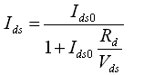
where Ids0 is the drain current without the resistance effect and
The selection of the resistance model is summarized here:
CORSRD = 1 : solved by circuit simulator with internal nodes
RDVG11, RDVG12, RDVB, RDS, RDSP, NRD
RD, RDVD, RDVDL, RDVDLP, RDVDS, RDVDSP
RDSLP1, RDICT1, RDSLP2, RDICT2, RDOV11, RDOV12, RDOV13
CORSRD = 2 : solved with the analytical approach
RD21, RD22, RD22D, RD23, RD23L, RD23LP
RD23S, RD23SP, RD24, RD25, RD20
CORSRD = 3 : Both CORSRD = 1 and CORSRD = 2 are considered.
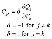
Capacitance
Intrinsic Capacitance
The intrinsic capacitances are derivatives of the node charges determined as
Overlap Capacitance
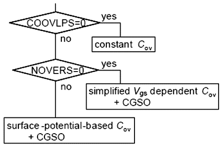
Three different overlap capacitance models are supplied to modeling the overlap capacitance: Constant model, Simplified model and Surface-potential-based model. Flag COOVLP ( COOVLPS ) and NOVER ( NOVERS ) are used to select the corresponding model.
Figure -7 Model options of the overlap capacitance at the drain side are summarized.
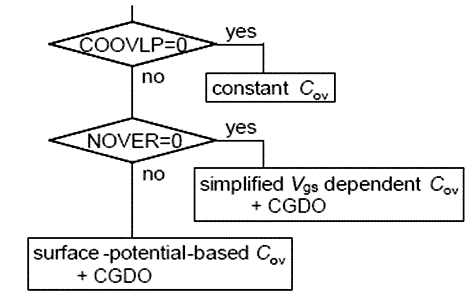
Figure -8 Model options of the overlap capacitance at the source side are summarized.
Leakage Currents
Substrate Current
The substrate current Isub is generated by impact ionization in the depletion region at the drain junction
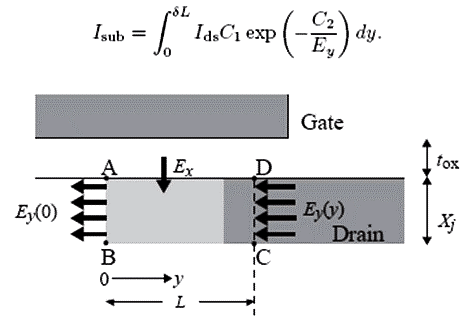
where C1 and C2 are fitting parameters.
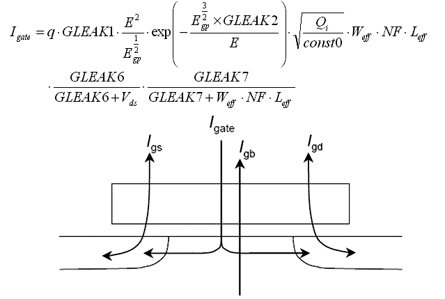
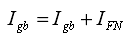
Gate Current
All possible gate leakage currents are schematically shown in Fig. 32.8
Between Gate and Channel, Igate
The Igb current under the accumulation condition is modeled as
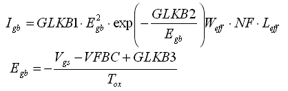
The Fowler-Nordheim tunneling mechanism is also considered
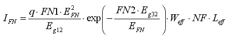
Total substrate current is the sum of the two components as
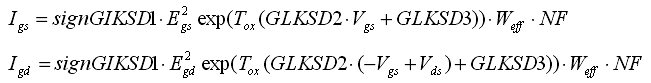
Between Gate and Source/Drain, Igs/Igd
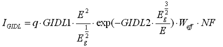
GIDL (Gate-Induced Drain Leakage)
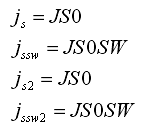
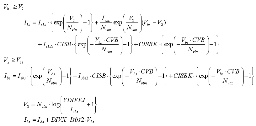
Source/Bulk and Drain/Bulk Diode Models
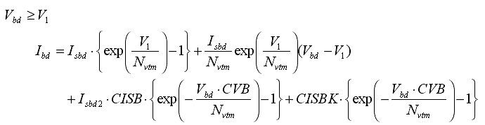
Between Drain and Bulk
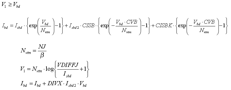
Between Source and Bulk
Noise Models
1/f Noise Models
The 1/f noise is caused by both the carrier fluctuation and the mobility fluctuation. The final description for the drift-diffusion model is
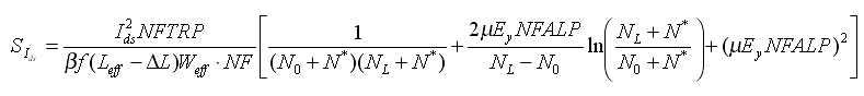
where the parameters NFALP and NFTRP represent the contribution of the mobility fluctuation and the ratio of trap density to attenuation coefficient, respectively.
Thermal Noise Model
Van der Ziel derived the equation for the spectral density of the thermal drain-noise current at temperature T by integrating the trans-conductance along the channel direction y based on the Nyquist theorem

where ?s, ?d and ?av are mobilities at the source side, the drain side, and averaged, respectively.
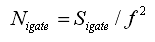
Induced Gate Noise Model
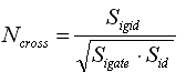
Coupling Noise Model
Non-Quasi-Static (NQS) Model
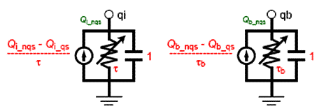
Formation of carrier
Carriers in the channel take time to build-up as opposed to the Quasi-Static (QS) approximation. To consider this phenomenon in HiSIM, the carrier formation is modeled as
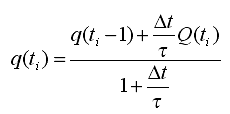
where q(ti) and Q(ti) represent the non-quasi-static and the quasi-static carrier density at time ti, respectively, and ![]() t = ti – ti-1 is valid. Above equation implies that the formation of carriers under the NQS approximation is always delayed in comparison to the QS approximation, which is the basic origin of the NQS effect.
t = ti – ti-1 is valid. Above equation implies that the formation of carriers under the NQS approximation is always delayed in comparison to the QS approximation, which is the basic origin of the NQS effect.
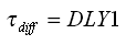
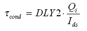
Delay Mechanisms
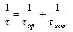
These two delay mechanisms (diffusion and conduction) are combined using the Matthiessen rule:
Applying the same approach for the formation of bulk carriers, leads to the approximation of the bulk carrier delay as an RC delay in the form
NQS model implementation into circuit simulator is listed as following figure:
Self-Heating Effect Model
The self-heating effect is modeled with the thermal network shown in the following figure. The flag COSELFHEAT must be equal to one and RTH0 must not be equal to zero to activate the model.
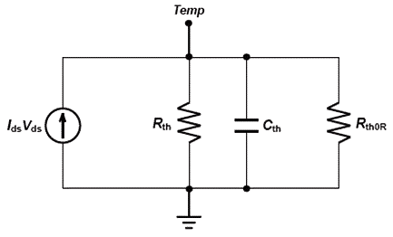
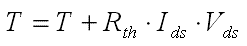
The total temperature of the devices is the sum of the original temperature and the temperature rise due to self-heating.
where Rth as well as Cth are a function of Weff as
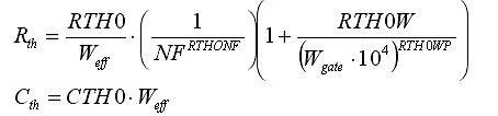
HiSIM HV 1.1.1 models the thermal dissipation in a different way with that of previous version as:
where POWRAT is a model parameter. The external node potential is represented by Vds and the internal node potential within the drift region at the channel/drift junction is by Vdsi, which is calculated during the simulation.
DFM Model
To support design for manufacturability (DFM) HiSIM introduces an option for considering the variation of device parameters.
Component Statements
Instance Parameters
Model Definition
model modelName hisim_hv parameter=value ...
Model Parameters
Device type parameters
Default for instance parameters
Basic Device Parameters
Temperature dependence effects
Quantum Mechanical Effects
|
Coefficient for quantum mechanical effect. Default as 0.0 for version 1.23, 2.0 for version 2.10. |
||
Poly Depletion Effects
Short Channel Effects
Narrow channel effects
|
Substrate-impurity concentration at the SIT edge, defaulted as 5e17 since version 2.10. |
||
Mobility Effects
Small size parameters
|
Threshold voltage shift of STI leakage due to small size effect. |
||
|
Threshold voltage shift of STI leakage due to small size effect. |
||
Channel Length Modulation Effects
Substrate Current Effects
Gate Current Effects
|
Parameter for gate current. The default value is 1e3 since version 2.00. |
||
|
Parameter for gate current. The default value is -1e3 since version 2.00. |
||
GIDL Current Effects
|
Parameter for GIDL. The default value is 0.0 for version 2.00/2.01 and version 1.23. |
||
Noise 1/f Effects
|
Flicker (1/f) noise contribution of the mobility fluctuation. |
||
|
Flicker (1/f) noise ratio of trap density to attenuation coefficient. |
||
Subthreshold swing parameters
NQS parameters
|
Minimum parasitic resistance, resistance smaller than minr will be clamped as minr. |
||
Symmetry for short-channel mosfet
P-N junctions parameters
Overlap capacitance parameters
Smoothing coefficient between linear and saturation
|
Coefficient of effective electric field. The default value is 10 for version 2.00/2.01 and 1.23. |
||
DFM parameters
Substrate model parameters
|
Impurity concentration of the substrate required for Vsub dependence. |
||
Operating region warning control parameters
|
Parameter to turn warnings on and off. Possible values are |
||
|
Drain diode breakdown voltage, take effect when bvj not given. |
||
|
Source diode breakdown voltage, take effect when bvj not given. |
||
Mismatch parameters
|
Mismatch mode selector. The available modes are 0, 1, 2 and 3. |
||
LDMOS special parameters
|
Lgate dependence of impurity concentration of the surface N^- layer. |
||
|
Lgate dependence of impurity concentration of the surface N^- layer. |
||
Auto Model Selector parameters
New Depletion Mode Parameters (since version 2.20)
New Hard BreakDown Voltage Parameters (since version 2.30)
Binning model parameters
Safe Operating Areas Parameters
Output Parameters
Operating-Point Parameters
|
Estimated operating region. Possible values are |
||
Parameter Index
In the following index, I refers to instance parameters, M refers to the model parameters section, O refers to the output parameters section, and OP refers to the operating point parameters section. The number indicates where to look in the appropriate section to find the description for that parameter. For example, a reference of M-35 means the 35th model parameter.
Return to top