Parameter Descriptions
Table -2
Process Parameters Group
|
Parameter
|
Unit
|
Description
|
Default
|
MIN
|
MAX
|
|
ITL
|
μm2
|
Interface states scaling factor
|
0
|
0
|
|
|
LPKT
|
μm
|
Pocket length
|
0
|
|
|
|
NP
|
cm-3
|
Polysilicon doping
|
1022
|
(See Note2)
|
None
|
|
NSUB
|
cm-3
|
Substrate doping
|

|
1015
|

|
|
QMC None
|
None
|
QM correction factor
|
0
|
0
|
|
|
TOX
|
m
|
Oxide thickness
|

|

|

|
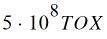
At present, PL = 0.2.
Table -3
Effective Geometry Group
|
Parameter
|
Unit
|
Description
|
Default
|
MIN
|
MAX
|
|
DL0
|
μm
|
Channel length offset
|
0
|
See Note3
|
|
DLL
|
μm2
|
Channel length adjustment (L)
|
0
|
|
DLW
|
μm2
|
Channel length adjustment (W)
|
0
|
See Note4
|
|
DW0
|
μm
|
Channel width offset
|
0
|
|
DWL
|
μm2
|
Channel width adjustment (L)
|
0
|
|
DWW
|
μm2
|
Channel width adjustment (W)
|
0
|
|
DWP
|
μm3
|
Channel width perimeter factor
|
0
|
|
DLQ
|
μm
|
Decoupling parameter
|
0
|

|
none
|
|
DWQ
|
μm
|
Decoupling parameter
|
0
|

|
none
|
Table -4
Mobility Group
|
Parameter
|
Unit
|
Description
|
Default
|
MIN
|
MAX
|
|
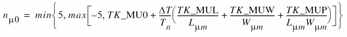
MU0
|

|
Low-field mobility
|
500
|
0.01
|
104
|
|
NU0
|

|
Non-universality factor
|
0
|
0
|
1
|
|
NUL
|

|
Non-universality factor (L)
|
0
|
See Note5
|
|
NUW
|

|
Non-universality factor (W)
|
0
|
|
MU1
|

|
Magnitude of the vertical field dependence
|
0.5
|
0
|
|
|
MU1W
|

|
Scaling parameter (W)
|
0
|
|
|
|
MU2
|
None
|
Sharpness of the vertical field dependence
|
1.5
|
0
|
3
|
|
MU3
|

|
Scaling parameter (W)
|
0
|

|

|
|
CS
|
None
|
Coulomb scattering
|
0
|
0
|
10
|
Table -5
Series Resistance Group
|
Parameter
|
Unit
|
Description
|
Default
|
MIN
|
MAX
|
|
R0
|

|
Fixed component of series resistance
|

|
See Note6
|
|
R1
|

|
Scaling factor (L)
|
0
|
|
R2
|

|
Scaling factor (W)
|
0
|
|
R3
|
|
Scaling factor (L,W)
|
0
|
|
R4
|

|
Gate bias dependence
|
0
|
0
|
None
|
|
R5
|

|
Scaling factor (L) gate bias dependence
|
0.02
|
|

|
|
R6
|

|
Scaling factor (W) for gate bias dependence
|
0
|
See Note7
|
|
RB
|

|
Back bias factor
|
0
|
0
|
1.0
|
Table -6
Velocity Saturation Group
|
Parameter
|
Unit
|
Description
|
Default
|
MIN
|
MAX
|
|
VSAT
|
m/s
|
Saturation velocity
|
80,000
|
50,000
|
150,000
|
|
ST0
|

|
Gate bias dependence of saturation velocity
|
0
|
0
|
0.3
|
|
ST1
|

|
Adjustment of saturation velocity (W)
|
0
|
ST1min
See Note8
|
ST1max
See Note9
|
|
STX
|

|
Back bias dependence of saturation velocity
|
0
|
0
|
1
|
|
GH0
|
None
|
Grotjohn/Hofflinger (GH) factor
|
0.5
|
0.05
|
5
|
|
GH1
|

|
GH Scaling parameter (L-1)
|
0
|
See Note10
|
|
GH2
|

|
GH Scaling parameter (L-2)
|
0
|
|
GH3
|

|
GH Scaling parameter
(L-2W-1)
|
0
|
|
GH4
|

|
GH Scaling parameter
(L-2W-2)
|
0
|
|
AS0
|
None
|
Transition from triode to saturation
|
12
|
6
|
100
|
|
ASL
|
None
|
Scaling factor (L) for triode-saturation
|
0.6
|
See Note11
|
|
S0
|
None
|
Vdsat adjustment
|
0.98
|
0.9
|
0.99
|
Table -7
Flat-band Voltage Group
|
Parameter
|
Unit
|
Description
|
Default
|
|
FB0
|
V
|
Vfb for long wide devices

|
-1
|
|
FB1
|

|
Scaling parameter (W-1)
|
0
|
|
FB2
|

|
Scaling parameter (W-2)
|
0
|
|
FB3
|

|
RSE parameter (W-1)
|
0
|
|
FB4
|

|
RSE parameter (W-2)
|
0
|
|
FB5
|

|
RSE parameter (L-1)
|
0
|
|
FB6
|

|
RSE parameter (L-2)
|
0
|
|
FB7
|

|
RSE parameter (L-3)
|
0
|
There are no limits on flat-band voltage parameters.
Table -8
Lateral Gradient Factor Group
|
Parameter
|
Unit
|
Description
|
Default
|
MIN
|
MAX
|
|
FL1
|

|
Scaling parameter for F0
|
0.1
|
See Note12
|
|
FL2
|

|
Scaling parameter for F0
|
0.01
|
|
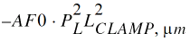
AF0
|

|
Scaling parameter for Af
|
0.004
|
0
|
10
|
|
AFL
|

|
Scaling parameter for Af
|
0
|
|
10
|
|
BFL
|

|
Scaling parameter for Bf
|
0.015
|
0
|
10
|
|
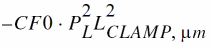
CF0
|

|
Scaling parameter for Cf
|
0.0005
|
0
|
10
|
|
CFL
|

|
Scaling parameter for Cf
|
0.01
|
|
10
|
|
KL
|

|
Scaling parameter for CLW
|
0
|
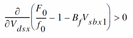
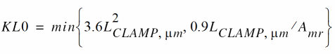
-KL0 (See Note13)
|
KLO
|
|
KW
|

|
Scaling parameter for CLW
|
0
|
|
10
|
|
DF
|
None
|
Sharpness of f(Vds) dependence
|
0
|
0
|
3
|
|
EF
|
None
|
Sharpness of f(Vsb) dependence
|
0
|
0
|
3
|
Table -9
Channel Length Modulation Group
|
Parameter
|
Unit
|
Description
|
Default
|
MIN
|
MAX
|
|
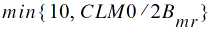
CLM0
|
None
|
Lq2d parameter
|
0.1
|
0
|
none
|
|
CLM1
|

|
Lq2d scaling parameter (L)
|
0
|
|
|
|
CLM2
|

|
Lq2d scaling parameter (W)
|
0
|
|
|
|
CLM3
|

|
Logarithm dependence factor
|
10
|
0
|
1000
|
|
GDL
|

|
Scaling parameter (L)
|
0
|
0
|
0.9
|
New Parameters for SPMOS Version 34
The following parameters have been added to version 34.
I
|
Parameter
|
Unit
|
Description
|
Default
|
MIN
|
MAX
|
|
NCG
|
|
Instance parameter for factor of Rgate
|
1
|
1
|
2
|
|
SW_GIDL
|
|
Flag og gidl
|
0
|
0
|
1
|
|
IT0
|
|
Interface states scaling factor
|
0
|
0
|
2
|
|
NPKT
|
um
|
Effective doping parameter
|
1.0
|
0
|
2
|
|
NSLP
|
1/V
|
Effective doping parameter
|
0
|
0
|
2
|
|
YPKT
|
|
Effective doping parameter
|
0.001
|
0.001
|
2
|
|
VNSUB
|
V
|
Effective doping parameter
|
0
|
|
|
|
GDS1
|
|
Vds dependence of Gds slope
|
0
|
|
|
|
GDS2
|
|
Vds dependence of Gds slope
|
0
|
|
|
|
GDS1L
|
1/
|
Scaling parameter for Hlo1
|
0
|
|
|
|
GDS2L
|
1/
|
Scaling parameter for Hlo2
|
0
|
|
|
|
GDS1A
|

|
Scaling parameter for Hlo1
|
0
|
|
|
|
GDS2A
|

|
Scaling parameter for Hlo1
|
0
|
|
|
|
TK_BGIDL
|
1/K
|
Temperature dependence
|
0.0
|
0.0
|
1.0
|
|
TK_IIA2
|
|
Substrate current scaling parameter
|
0.0
|
0.0
|
1.0
|
|
KGOV
|
|
Decouples tunneling and CV overlap fitting
|
1
|
0.1
|
10
|
|
CHIB
|
eV
|
Band offset
|
3.13
|
2.5
|
4
|
|
AGIDL
|
|
IGIDL coefficient
|
0.7
|
0
|
|
|
BGIDL
|
V
|
Tunneling barrier adjustment
|
28
|
1
|
100
|
|
CGIDL
|
1/V
|
Lateral field dependence
|
0.007
|
0
|
1
|
|
IIA1W
|
 /V1/2
/V1/2
|
Substrate current scaling parameter
|
0
|
-1
|
1
|
|
IIA1P
|
 /V1/2
/V1/2
|
Substrate current scaling parameter
|
0
|
-1
|
1
|
Parameters with Different Default Values for SPMOS Version 34
|
Model Parameter
|
Old Default Value
|
New Default Value
|
|
noia
|
0.0
|
1.0e+20
|
|
noib
|
0.0
|
5.0e+04
|
|
noic
|
0.0
|
1.4e-12
|
Instead of limiting TK_MU0, TK_MUL, TK_MUW and TK_MUP, SPMOS sets
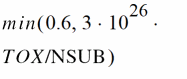
Setting NP=0 or NP > 1028m-3 turns off polysilicon depletion effect.
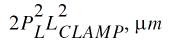
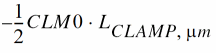
Instead of limiting the values of DL0, DLL and DLW, SPMOS sets the channel length offset as
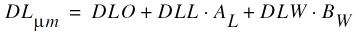
and the effective channel length (in μm) as

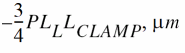
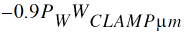
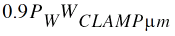
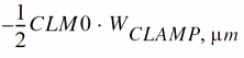
Instead of limiting parameter values of DW0, DWL, DWW and DWP, SPMOS sets the channel width offset as

and the effective channel length (in μm) as

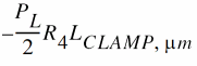
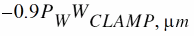
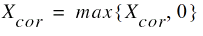
At present,
P
w=1/4.
Instead of limiting NU0, NUL and NUW, SPMOS sets
Instead of limiting the values of R0, R1, R2, and R3, SPMOS sets

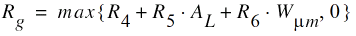
Instead of limiting the values of R6, SPMOS sets


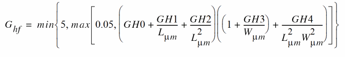
Instead of limiting the values of GH1, GH2, GH3, and GH4, SPMOS forces Ghf to be in the range [0.05, 5]
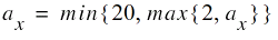
Instead of limiting the values of ASL, SPMOS forces ax to be in the range [2,20]
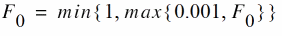
Instead of limiting the values of FL1 and FL2, SPMOS forces F0 to be in the range [0.001, 1]
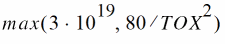
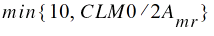
Instead of limiting the values of GDS1 and GDS2, SPMOS forces
 Return to top