Via Snapping
Custom layout designs can contain stdVia, cdsViaDevice, cdsGenVia, and customVia types of vias. Except for customVias, none of the vias insert a snap pattern shape into the via subMaster. Therefore, vias are snapped based on the shapes they contain, instead of a snap pattern. Also, when a via in a via stack is snapped to a snap pattern shape, the entire via stack is snapped. A via stack is snapped as a group. Via and via stacks that overlap a matching snap pattern shape after a copy, move, or create operation are snapped to the grid.
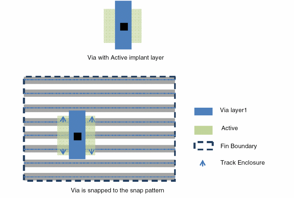
For example, consider a FinFET process where snap pattern shapes are used for fin boundaries. When a via containing an Active shape is placed on a fin boundary, it is automatically aligned to the fin grid based on the enclosures of the snap pattern shape. The following figure contains a via with a layer on Active/drawing. When the via is moved over a snap pattern shape that applies to all Active shapes, the via is automatically snapped to the fin grid based on the enclosures attribute of the snap pattern.
When a snapPatternDef does not have any snapPurposes, it applies to all shapes on the snapLayer.
If the snap pattern applies to shapes on multiple LPPs and the via master contains shapes on several such LPPs, the snapping algorithm performs snapping based on one of the LPPs.
If the via overlaps multiple snap pattern shapes that are Active, then the snapping algorithm performs snapping based on one snap pattern shape.
Snap pattern shapes on the same LPP must snap to each other. Snapping should be performed after a copy, move, or stretch operation or creation of an instance or a via.
You can use the environment variables and to specify the snap depth and the method used to define the snap depth for snap pattern snapping, respectively.
Related Topics
Object Snapping to Local Snap Pattern Shapes
Return to top