Troubleshoot Layout XL Compliance
You can face following issues related to Layout XL Compliance:
- Issues Faced when Setting up the PDK to Improve Layout XL Compliance
- Resolving Terminal Mismatches between Schematic and Layout
- Issues when Editing the CDF to Add Permute Rules
Issues Faced when Setting up the PDK to Improve Layout XL Compliance
The troubleshooting information in this section is targeted at CAD team or library owners who can implement the recommended set up at the PDK level so that the benefits of these global updates can be experienced by all the layout engineers using the library.
Prerequisites
- A layout with pins and cells or Pcells that can be bound to schematic counterparts.
- An LVS-clean layout that can use physical connectivity to establish the required schematic versus layout bindings.
The table below lists some likely layout issues that a CAD team member or a Library owner can resolve at the global level:
| Layout issue | Impact | How to resolve... |
|---|---|---|
|
Shorts reported in the layout during Update Binding or during a Layout XL-compliance check |
Edit the Component Description Format (CDF) to add the missing permute rule. For information on what permute rules are and why it is important to set these correctly to create a layout that is Layout XL compliant, see Issues when Editing the CDF to Add Permute Rules. |
|
|
Shorts reported in the layout during extraction of shapes at the level below the specified extraction level |
Edit the technology file to define stop layers. For information on what stop layers are and why it is important to set these correctly to create a layout that is Layout XL compliant, see Issues when Editing the Technology File to Add Stop Layers. |
|
|
Edit the Library Attributes Mapping (LAM) file to add missing component types and resolve terminal mismatches between the schematic and the layout. For information on editing the LAM file, see Library and Attributes Mapping File Syntax. |
Issues when Editing the CDF to Add Permute Rules
Layout XL being connectivity-aware, it expects a net to be connected to the correct terminal. Else, a short is reported.
If you bring a layout created outside of Layout XL into Layout XL, it is likely that the layout will have its S and D (or the n and p terminals) connected interchangeably. This can cause shorts to be reported during an Update Binding run as the connectivity will be considered as incorrect in Layout XL. To resolve this, you can create permute rules for any devices that are likely to be connected in this manner.
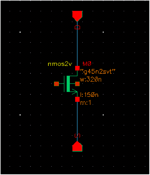
Consider the following example. Here a schematic with a single nmos2v device has its net D connected to terminal D and net S connected to terminal S, as shown in the figure below.
Let us assume that the layout was created outside Layout XL in a non-connectivity aware environment. Because the layout device is symmetrical and the logical connectivity from the schematic was not considered, you could connect the nets S and D to either side of the device.
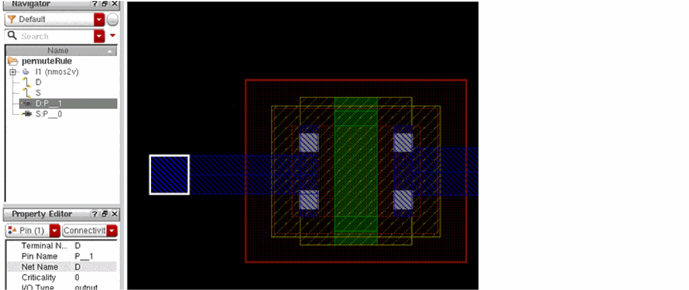
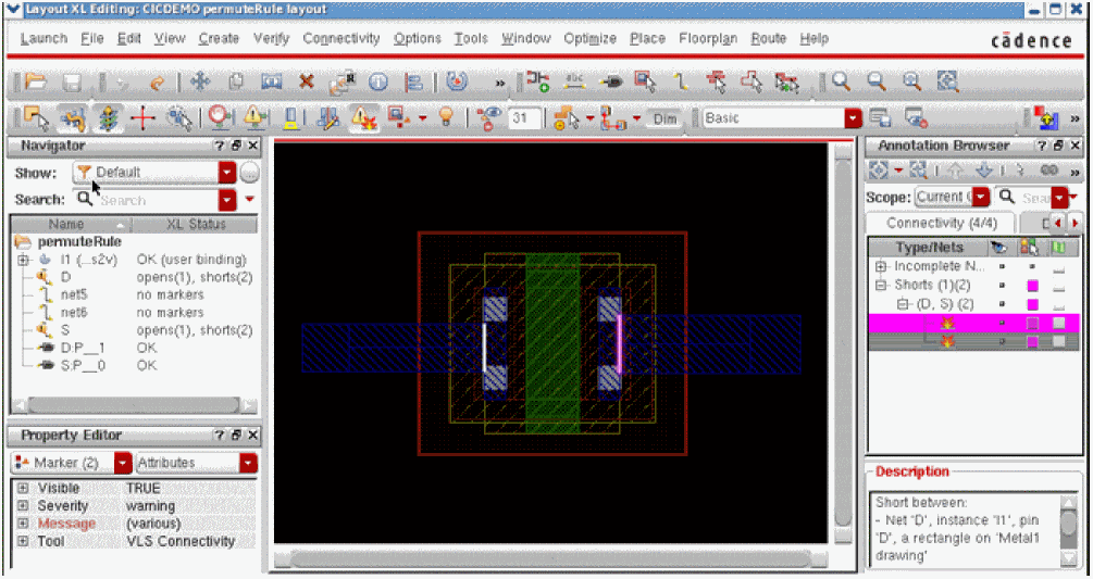
If we open the layout in Layout XL, the device connectivity will be considered. If the layout net D is connected to the S terminal, the physical connectivity (routing) is found to be different from the logical connectivity in the schematic. This results in opens and shorts being reported because the terminals are incorrectly connected, as shown in the figure below.
However, if it is acceptable to connect the terminals S and D interchangeably, we must specify the same using the appropriate CDF permute rule before launching the design in Layout XL.
-
Close the layout window, if open, and in the CIW, choose Tools – CDF – Edit.
The Edit CDF form displays, as shown below.
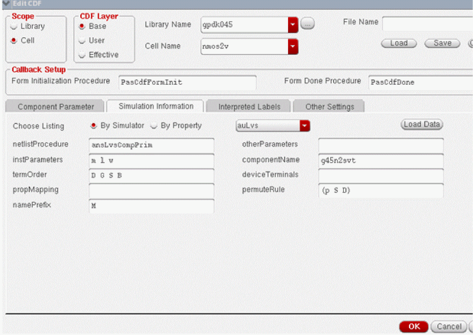
- Set the value for Scope to Cell.
- Set the value for CDF Layer to Base.
-
Specify the Library Name and Cell Name.
For this example: - Select the Simulation Information tab.
- Select auLvs from the drop-down menu adjacent to Choose Listing.
- In the permuteRule field, type the permute rule, such as (p S D).
- Click OK.
For the CDF permute rule updates to take effect, open the design in Layout XL.
When the nmos2v is used in Layout XL, its S and D terminals can be connected interchangeably with no opens or short created, as shown below.
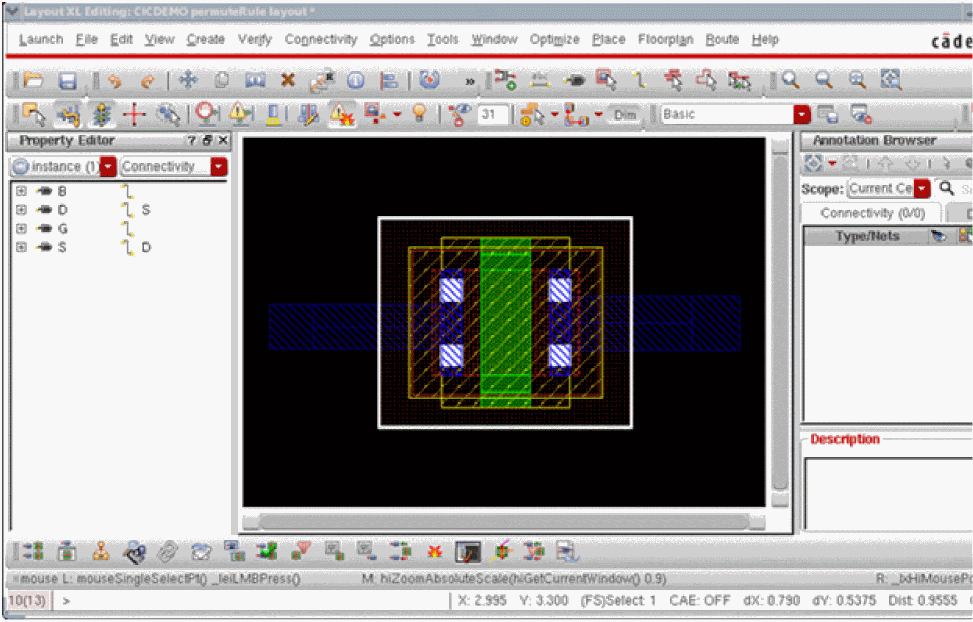
Additionally, when running Update Binding, it will use the permute rule, if required, to get the correct connectivity and increase the XL-compliance of the layout.
For more information on adding permute rules, see permuteRule Property.
Issues when Editing the Technology File to Add Stop Layers
In Layout XL, an extraction stop level 0 is sufficient to establish the connectivity, if connections are made to the pins of cells at the level below. However, if these connections are not made to the pins, the extraction level needs to be increased to consider the shapes at the level below.
Layout XL now has the capability to extract through all the extractable shapes in the level below the specified extraction level. However, this can lead to shorts because the lower-levels cells were not originally created to support extraction. Therefore, a stopLayer may have to be defined to stop the extraction at the defined shape, and prevent a short being created.
Consider a layout that contains:
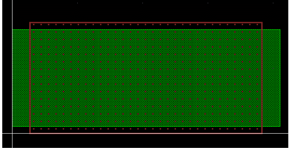
The figure below represents cell I0 containing a poly shape (green) and a resdum shape (red dots).
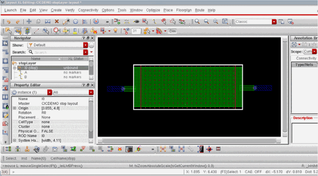
At the top level (level 0), routes are created from Pins A and B to connect to the poly shape in cell I0. If we extract at level 0 by setting the Options – Connectivity – Connectivity – Hierarchy Control to 0, no short is created between nets A and B, as shown below. This is so because the poly shape in I0 is at level 1, therefore, not considered for extraction.
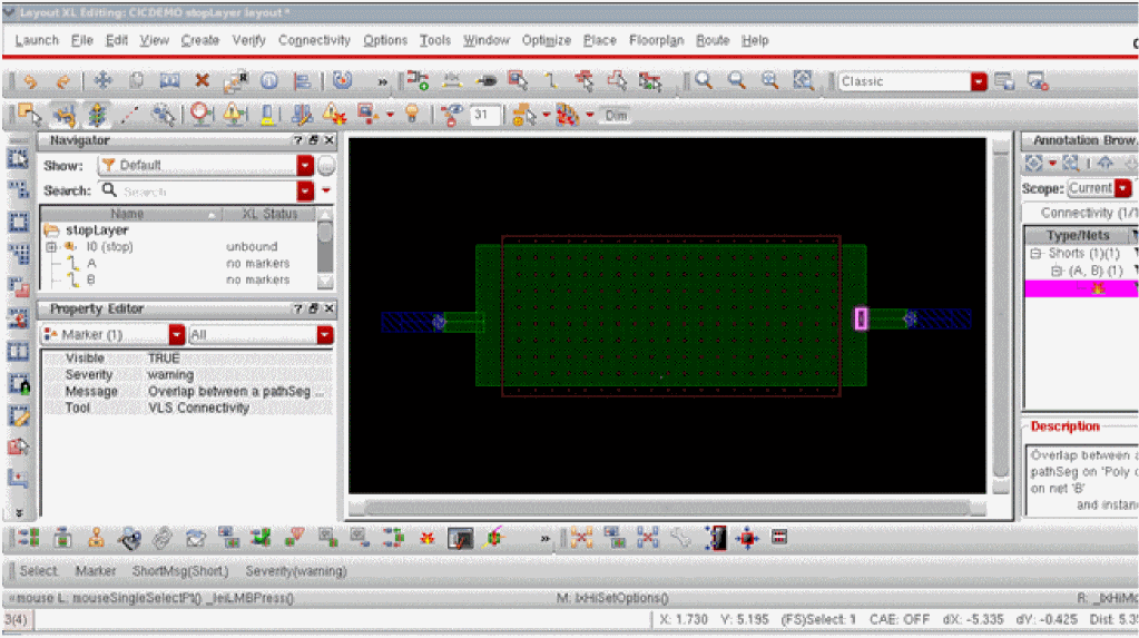
However, if the extraction depth is increased to 1 and the extractor is run again, a short is created between net A and B, as shown below. This is expected because the extractor now considers the poly shape within I0 as the extraction depth has been increased.
Although extracting at level 0 can prevent reporting shorts to lower levels, in some situations such as when finding off-pin connected at the level below, the extraction depth may need to be increased. This results in shorts being created. To avoid the shorts, a stop layer must be defined in the technology file. This can either be a real layer or a derived one.
For more information on adding stop layers, see validLayers – Stop Layers Specification.
Editing the LAM File to Increase Layout XL Compliance
What is a LAM file?
The Library and Attributes Mapping file—LAM file (cph.lam)—stores the schematic and layout library data, such as:
- symbol properties that drive layout generation
- component type information for a given library
- library and cell-level mapping information
The cph.lam file is stored in the design hierarchy at: library/.cadence/dfII/cph/lam/cph.lam
Currently, there is no graphical user interface available to help you create or edit a LAM file. Therefore, a new file or any edits should be created using your preferred text editor.
The values you set in the LAM file can also be set in Configure Physical Hierarchy (CPH), but if set in CPH, they are written to the physConfig view and will only apply to the current design. Setting the values in the LAM file ensures that every user benefits from the setting.
For more information on CPH, see Physical Hierarchy Configuration. For more information on the LAM file, see Library and Attributes Mapping File Syntax.
The values that can be set in a LAM file are:
-
Component types – Layout XL uses component types to identify devices. For example,
nmosandpmoscomponent types are used to identify the device terminals for Update Binding. Additionally, the width parameter and the folding threshold are used by automatic folding.
If the disableFolding environment variable is set and the folding threshold for the component type is set to0, folding is disabled. - Terminal mapping between the schematic and the layout – Often there are terminal mismatches between schematic and layout and these are reported as connectivity differences in Layout XL. This terminal mismatch can also prevent Update Binding from giving a good result.
Setting Component Types in LAM
The setting of component types is recommended to help identify devices in Layout XL. It is good practice to define a component type for at least nmos and pmos devices and then map the appropriate cells to the component type, before the library is released to users.
The setting of component types allows the Update Binding command to recognize devices and their terminals.
Consider the following example. In the gpdk045 library there are two cells: nmos2v and pmos2v. To identify these devices as nmos and pmos devices respectively, we can create component types in the LAM file and map the cells to the correct component type. The following section of the sample LAM file illustrates this:
<PHYSICAL>
<COMPONENT_TYPE_GROUPS>
<LIB NAME="gpdk045">
<COMPONENT_TYPE_GROUP NAME="nmos">
<COMP_CLASS>NMOS</COMP_CLASS>
<WIDTH>fw</WIDTH>
<DRAIN>D</DRAIN>
<GATE>G</GATE>
<SOURCE>S</SOURCE>
<BULK>B</BULK>
<ACTIVE_LP>Oxide drawing</ACTIVE_LP>
<FOLD_THRESH>1e-06</FOLD_THRESH>
</COMPONENT_TYPE_GROUP>
<COMPONENT_TYPE_GROUP NAME="pmos">
<COMP_CLASS>PMOS</COMP_CLASS>
<WIDTH>fw</WIDTH>
<DRAIN>D</DRAIN>
<GATE>G</GATE>
<SOURCE>S</SOURCE>
<BULK>B</BULK>
<ACTIVE_LP>Oxide drawing</ACTIVE_LP>
<FOLD_THRESH>1e-06</FOLD_THRESH>
</COMPONENT_TYPE_GROUP>
</LIB>
</COMPONENT_TYPE_GROUPS>
<MAPPINGS>
<LIB NAME="gpdk045">
<CELL NAME="nmos2v">
<COMPONENT_TYPE>
<NAME>nmos</NAME>
<LIB>gpdk045</LIB>
</COMPONENT_TYPE>
</CELL>
<CELL NAME="pmos2v">
<COMPONENT_TYPE>
<NAME>pmos</NAME>
<LIB>gpdk045</LIB>
</COMPONENT_TYPE>
</CELL>
</LIB>
</MAPPINGS>
</PHYSICAL>
The sample above is a partial LAM file. To view a complete LAM file, see Example – Complete LAM File.
In our example, the nmos and pmos cells are in the gpk045 library. The LAM file for this library will be automatically read when Layout XL is opened, and you can view it using the CPH window. In CPH, you can verify if the LAM file settings you made are correct.
To verify the LAM file update in CPH:
-
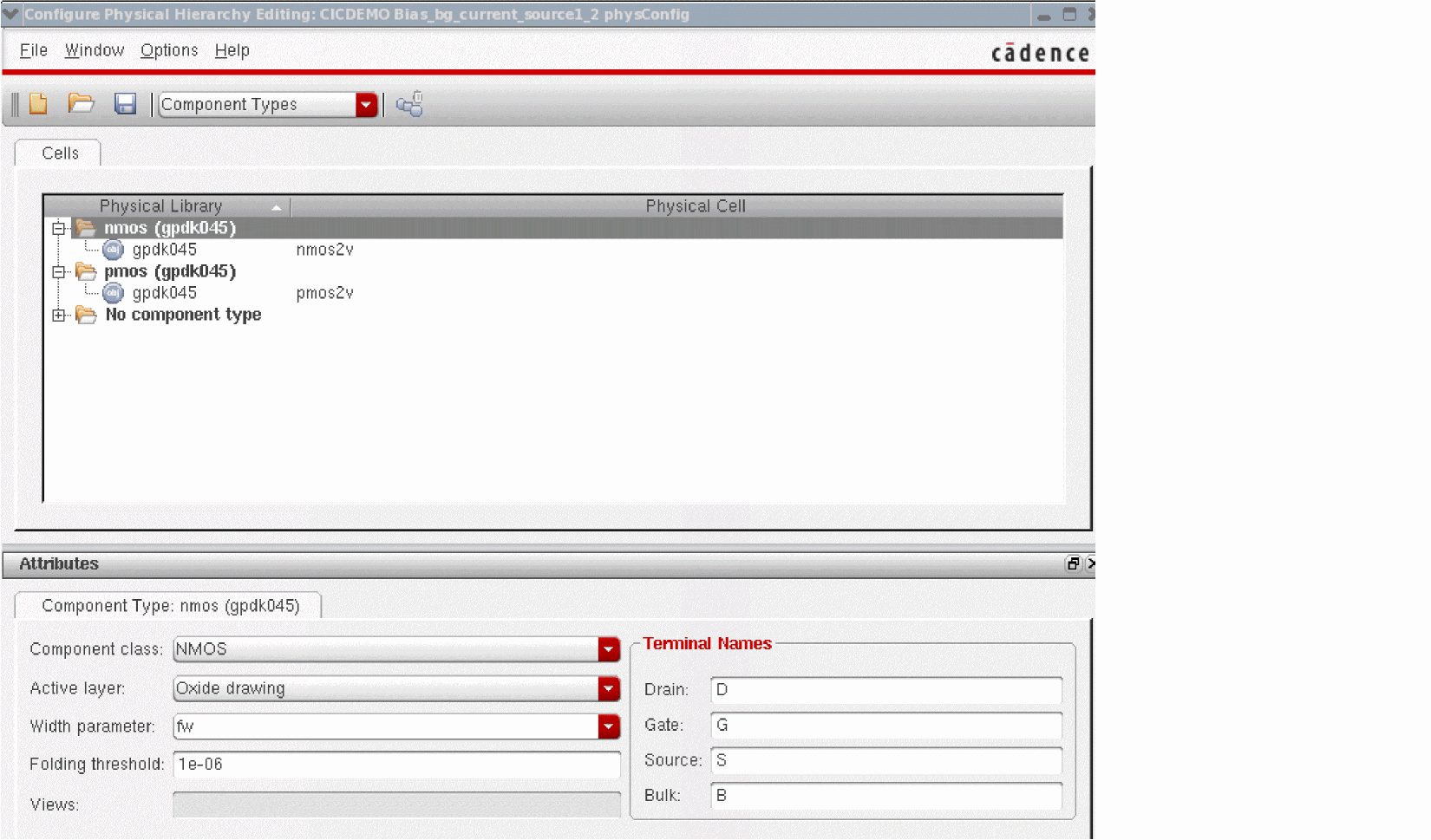
Choose Launch – Configure Physical Hierarchy.
The Configure Physical Hierarchy window displays. - Select Component Types from the drop-down menu at the top of the window.
The CPH window displays the two component types – nmos and pmos – that you added using the LAM file, as shown in the figure below.
Resolving Terminal Mismatches between Schematic and Layout
Consider the example below. In the gpdk045 library, there is a cell resnspoply. As can be seen in the screenshow below, the schematic has 3 terminals: B, MINUS and PLUS while the layout has 2 terminals: MINUS and PLUS. This causes Layout XL to report a connectivity difference, as seen in the XL Status column of the Navigator.
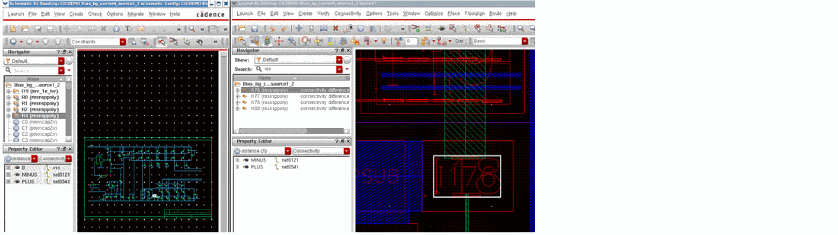
The connectivity difference displayed in the figure above can also cause the Update Binding command to result in bad bindings. Therefore, it is good practice to resolve terminal mismatches between the schematic and the layout using the LAM file before running the Update Binding command.
To stop the connectivity differences from being reported, you can add an ignore for generation property to the B terminal in the library LAM file, as shown below.
In the previous example, we had to edit the physical section of the LAM file to set up the component types. In this example, we are defining how the layout is generated from the schematic. Therefore, we need to edit the logical section of the LAM file.
<LOGICAL>
<LIB NAME="gpdk045">
<CELL NAME="resnsppoly">
<VIEW NAME="symbol">
<PARAMETERS>
<IGNORE>
<CHECK></CHECK>
<GEN></GEN>
</IGNORE>
</PARAMETERS>
<TERMINALS>
<IGNORE>
<CHECK></CHECK>
<GEN>B</GEN>
</IGNORE>
</TERMINALS>
</VIEW>
</CELL>
</LIB>
</LOGICAL>
The sample above is a partial LAM file. To view a complete LAM file, see Example – Complete LAM File. To verify if the LAM file is set correctly, you can verify the settings in the Configure Physical Hierarchy window.
To verify the LAM settings in CPH:
-
Launch – Configure Physical Hierarchy.
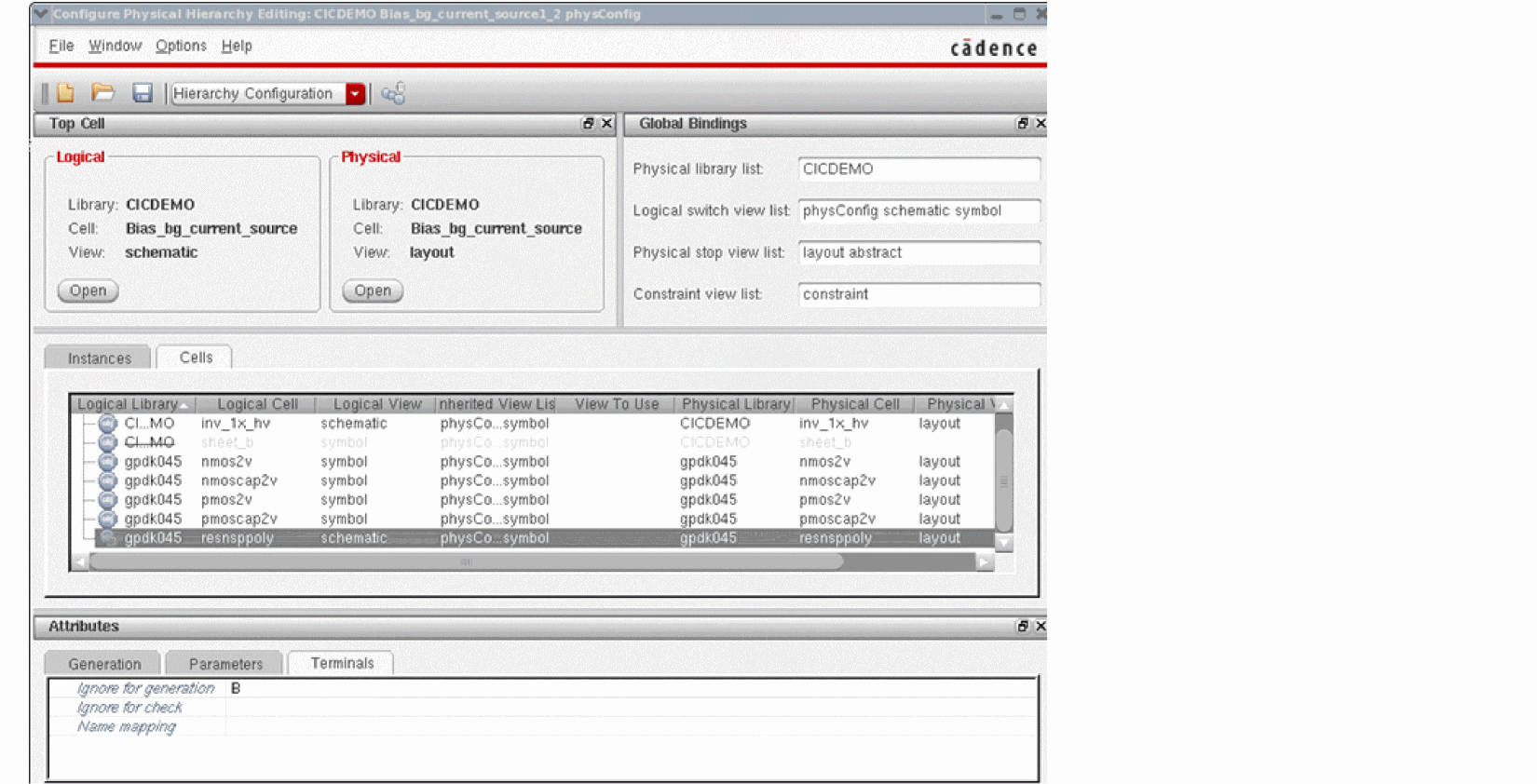
The Configure Physical Hierarchy form opens in Hierarchy Configuration mode. - In the middle pane, select the Cells tab and then select the resnsppoly entry in the table.
-
In the Attributes tab at the bottom of the window, select the Terminals tab, as displayed in the figure below.
-
Notice that the Ignore for generation property displays on terminal
B, as set in the LAM file.
After editing the LAM file, if you open a cellview in Layout XL and generate a resnsppoly device from the schematic, it will no longer report a connectivity difference. This is because the B terminal is now ignored, as shown in the figure below.
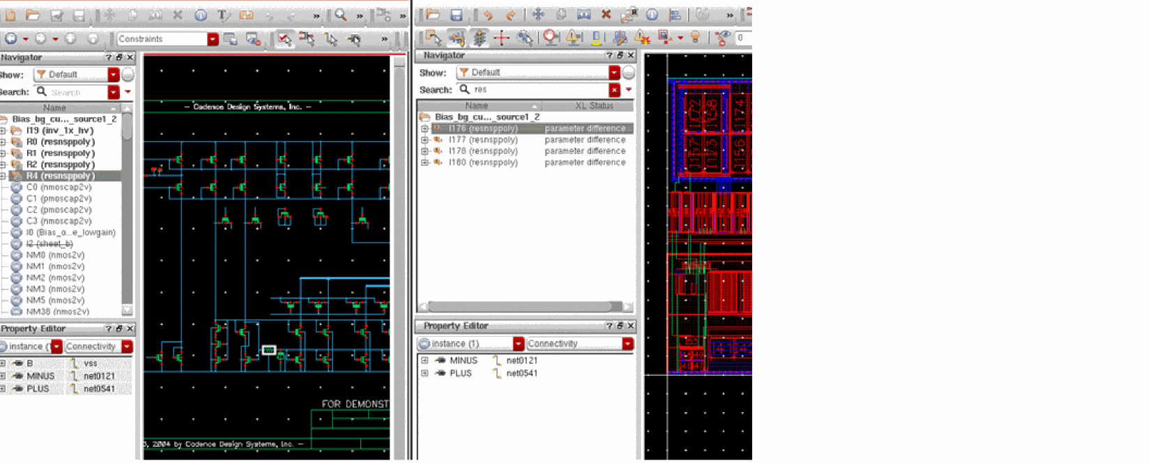
In the two Update Binding examples illustrated above, the XL status still reported parameter differences, although the binding and connectivity was correct. These differences should be checked, and if needed, an ignore property can be set for these in the Parameters section in the LAM file.
The sample LAM file below illustrates the use of the ignore property in the Parameters section.
<PARAMETERS>
<IGNORE>
<CHECK>sa sb leftTap RightTap</CHECK>
<GEN>simM</GEN>
</IGNORE>
</PARAMETERS>
Example – Complete LAM File
The sample below represents a complete LAM File that is set to improve the Layout XL compliance for a design.
<!DOCTYPE LAM_FILE>
<LIBRARY_DATA>
<VERSION NUMBER="0.2" />
<LOGICAL>
<LIB NAME="gpdk045">
<CELL NAME="resnsppoly">
<VIEW NAME="symbol">
<PARAMETERS>
<IGNORE>
<CHECK></CHECK>
<GEN></GEN>
</IGNORE>
</PARAMETERS>
<TERMINALS>
<IGNORE>
<GEN>B</GEN>
</IGNORE>
</TERMINALS>
</VIEW>
</CELL>
</LIB>
</LOGICAL>
<PHYSICAL>
<COMPONENT_TYPE_GROUPS>
<LIB NAME="gpdk045">
<COMPONENT_TYPE_GROUP NAME="nmos">
<COMP_CLASS>NMOS</COMP_CLASS>
<WIDTH>fw</WIDTH>
<DRAIN>D</DRAIN>
<GATE>G</GATE>
<SOURCE>S</SOURCE>
<BULK>B</BULK>
<ACTIVE_LP>Oxide drawing</ACTIVE_LP>
<FOLD_THRESH>1e-06</FOLD_THRESH>
</COMPONENT_TYPE_GROUP>
<COMPONENT_TYPE_GROUP NAME="pmos">
<COMP_CLASS>PMOS</COMP_CLASS>
<WIDTH>fw</WIDTH>
<DRAIN>D</DRAIN>
<GATE>G</GATE>
<SOURCE>S</SOURCE>
<BULK>B</BULK>
<ACTIVE_LP>Oxide drawing</ACTIVE_LP>
<FOLD_THRESH>1e-06</FOLD_THRESH>
</COMPONENT_TYPE_GROUP>
</LIB>
</COMPONENT_TYPE_GROUPS>
<MAPPINGS>
<LIB NAME="gpdk045">
<CELL NAME="nmos2v">
<COMPONENT_TYPE>
<NAME>nmos</NAME>
<LIB>gpdk045</LIB>
</COMPONENT_TYPE>
</CELL>
<CELL NAME="pmos2v">
<COMPONENT_TYPE>
<NAME>pmos</NAME>
<LIB>gpdk045</LIB>
</COMPONENT_TYPE>
</CELL>
</LIB>
</MAPPINGS>
</PHYSICAL>
</LIBRARY_DATA>
Return to top