A phase locked loop (PLL) example demonstrates the wreal modeling approach in a more complex scenario. The PLL was designed in the Virtuoso Schematic environment. The following is the top-level schematic.
Figure 4.1: Top-Level Schematic of PLL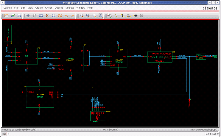
Let us now see the functions of all the blocks in the PLL. The upper left block is the reference clock generator, for example, a crystal oscillator. The next block, PHD, is the phase detector that compares the phase of the oscillator with the phase of the signal inside the PLL loop. Depending on which signal is first in terms of phase it creates a signal on one or the other output pin. The next block is the charge pump (CP). A charge pump translates the PHD output signals in a small amount of charge that is pumped into or pulled out of the following low pass filter (LPF). In a perfectly locked PLL, the output of the charge pump would have a constant voltage. If the frequency of the PLL is too small according to the reference, the output voltage is increased a bit. If it is too high, the voltage level is decreased. The LPF block is filtering out high-frequency portions of the signal to stabilize the loop. Finally, the voltage-controlled oscillator (VCO) is generating the output signal. This signal might have a higher frequency, for example, three times higher, as the input reference. To close the loop, the VCO output frequency is divided by this factor, 3 in the example. Now the reference signal and the downscaled output frequency can be compared in the PHD as shown in the above figure.
The two additional blocks on the schematic are a frequency measurement block on the extreme right-hand side and the source of all the power and reference signals at the bottom.
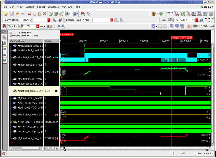
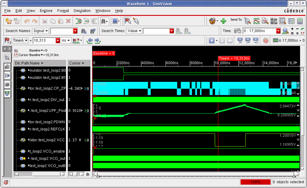
The PLL starts in a divide by 2 modes resulting in a 1.6 GHz output frequency given the 800 MHz reference clock. At about 2.5us the mode switches to a divide by 3, thus, the output frequency stabilizes at 2.4 GHz after some time. Now the supply voltage drops in three steps from 1.2 V down to 1.17 V where the VCO cannot deliver the 2.4 GHz anymore and the PLL goes out of the lock. It recovers after the VCC voltage rose again.
The following example illustrates the supply block.
`include "disciplines.vams"`timescale 100ps / 10psmodule supply ( B0, B1, PDWN, VCC, VCO_enable, VSS, i_bias );
wreal i_bias[1:0]; wreal VCC; wreal VSS;
parameter real pvcc = 1.2;
real v_supply;
assign i_bias[1] = 50u; assign i_bias[0] = 50u; assign VCC = v_supply;
initial begin // initial settings v_supply = pvcc; #25000 // after another 2.5 us reduce v_supply v_supply = v_supply - 0.01; #25000 // after another 2.5 us reduce v_supply v_supply = v_supply - 0.01; #25000 // after another 2.5 us reduce v_supply v_supply = v_supply - 0.01; #25000 // after another 2.5 us recover VCC v_supply = pvcc; endendmodule
Let us now focus on the power supply pin VCC. It is defined as an output of type wreal. Internally, we use a real variable v_supply to assign the different voltage levels at specific time points – as we would do in pure digital Verilog. We assign the v_supply real variable to the real-wire VCC. Note the concept of event-based changes of the values at specific time points (discrete-time).
Another important observation is that the wreal values have no unit. While we intuitively think of VCC being a voltage level – which is in reality – but it is not specified explicitly. The wreal port just carries a real value without a unit.
Wreal also supports arrays as shown above. In this case, two bias current values for the charge pump are defined in the supply module. The use of arrays follows the Verilog concept and syntax.
The following example illustrates the use of X and Z states. The concept of an unknown – X and high impedance – Z state that is used in the 4-state logic is useful for wreal signals as well. The meaning of X and Z is equivalent to the wreal case. The charge pump example uses the X value in case the enable signal is low:
always @(ENABLE,upReal,dnReal,I_out) begin // calculate up or dn current values based // on the validity of supply // and enable signals if (ENABLE===1'b1) begin iup = (upReal>0) ? IUPscale*I_out : 2u; idn = (dnReal>0) ? IDNscale*I_out : 2u;
end
else begin iup = `wrealXState; idn = `wrealXState; end end
The following schematic figure shows the outputs of the charge pump (Zp, Zn) connecting to the single filter input. Diving into the charge pump source code, the result was that both the output values are actively driven:
assign ZP = iup; assign ZN = -idn;
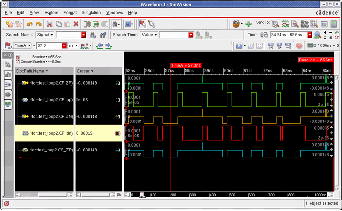
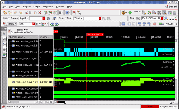
In the time point shown above, iup drives the net CP_ZP to a value of 2 u while idn drives the same net to 0.15 m. This results in a conflict since two drivers are driving the net at the same time toward different values.
The concept of wreal resolution functions resolves this limitation. In the simulation, when the -wreal_resolution sum switch is specified to xrun, it resolves the connected net to the sum of both values. In the original design, this CP_ZP node was a current summing node connecting the two charge pump outputs. To mimic this behavior in wreal, the above resolution function sum is used.
Another useful enhancement is the $table_model function known from analog Verilog-A and Verilog-AMS blocks. The function is now available for real values as well. The table model function enables an easy calibration of a real value behavioral model against measured data provided as a text file. The VCO in this example uses this capability.
real input_value; always @(LVDD_VCO_1p2, LGND_VCO, VCTRL) begin input_value = (LVDD_VCO_1p2 - LGND_VCO); tableInstantaneousFreq = $table_model(input_value, VCTRL, "vtuneFreqControl.tbl","1CC,3CC"); end
The example above calculates the VCO output frequency according to the table in the text file vtuneFreqControl.tbl. The text file contains the following data that is collected during the characterization of the original VCO.
#VDD VCNTL Freq1 0 9.81E+061 0.4 1.05E+091 0.8 1.41E+091.1 0 9.88E+061.1 0.45 1.29E+091.1 0.9 1.52E+091.2 0 9.95E+061.2 0.3 1.37E+091.2 1 2.69E+09...
Similar to the mechanism of automatically inserted connect modules (AICM) between the continuous and discrete domains (electrical/logic) are connect modules available between wreal and electrical. These are called E2R and R2E. They are also inserted automatically if needed during the elaboration process. That ensures an easy replacement of blocks from different types of representations. In this case, we changed the filter into an electrical filter to see results.
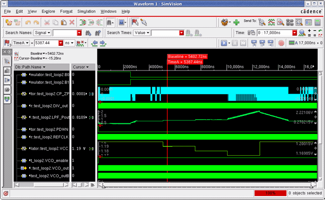
You might have noticed that the LPF_Pout value rises higher than the supply voltage in this case (around 12 us). This is a modeling artifact because we used an ideal charge pump with a wreal signal flow output (not feedback) that creates a current event though the voltage level is above the supply voltage range. In reality, the charge pump current would settle around the supply voltage level.
The IE Report message in the xrun logfile (use the –iereport option).
IE Report Summary: E2R ( electrical input; wreal inout; ) total: 1 ER_bidir ( wreal inout; electrical inout; ) total: 2---------------------------------------------------------------
Total Number of Connect Modules total: 3
The proper settings of the CM parameters are critical for correct simulation results, as we can see in the next exercise. If we change the vdelta parameter back to its default value of `Vsup/64:(... #(.vdelta(`Vsup/64) ...) the simulation results look quite different.
Vsub/64 results in about 0.028 V for the given supply of 1.2 V, thus, only changes larger than this value are creating events on the wreal net. Consequently, the first two supply voltage drops of 0.01 are not seen on the top-level VCC net.
Consider another scenario where we change the internal resistance of the R2E_2 and R2E_bidir CM back to their default value of 200 Ohm.
The electrical filter is consuming some amount of current from the VCC power supply that is generated from the wreal source. The power net is now connected by a 200 Ohm resistor to the wreal supply. This results in a significant IR drop on the VCC line and consequently in a changing VCC supply level. The simulation results are far from being correct anymore. As you saw in the last few simulations, the parameter settings of the wreal CM are critical and need to be set carefully to achieve good results.