Examples of analog models and how these analog models have been converted to pure wreal models to enable mixed-signal connections.
Voltage Controlled Oscillator
Consider the example of a voltage-controlled oscillator (VCO). VCO is a standard analog block that is used for examples in PLLs. It creates an output oscillation with a given frequency. This frequency can be modified to some range by the input voltage of the block.
The following testbench specifies that a real variable (r_in) is changed every 10ns from one value to another. The real variable is assigned to the wreal wire (w_in). This wreal signal is connected to the input port of the VCO block that is instantiated in the testbench.
`include "disciplines.vams"`timescale 1ns / 1ps
module top(); wreal w_in; real r_in; vco vco (w_in, clk);
always begin r_in = 1.0; #10 r_in = 1.2; #10 r_in = 0.2; #10 r_in = -0.2; #10 r_in = 1.345; #10 $finish; end assign w_in = r_in;endmodule
The VCO block takes the wreal input signal and calculates at each change of the signal (@(vin)) the required output frequency. Remember that the wreal signal is event based. That means that there are discrete events whenever the signal changes and the signal stay constant otherwise.
The calculated output frequency is used to determine the delay time between the clock inversion operations. Please note that the frequency settings depend on the timescale used. In this case, we used a 1ns timescale resulting in a 1 GHz frequency unit.
module vco(vin, clk); input vin; wreal vin; output clk; reg clk; real freq, clk_delay; real center_freq = 1; // freq in GHz real vco_gain = 1; // freq gain in GHz
initial clk = 0;
always @(vin) begin freq = center_freq + vco_gain*vin; clk_delay = 1.0/(2*freq); end always #(clk_delay) clk = !clk;endmodule
The following figure shows the simulation result for this example.
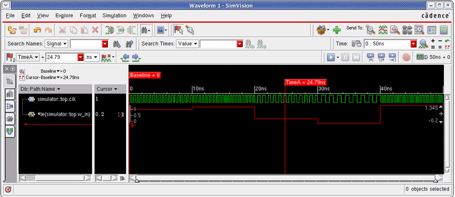
This is a simple example where there are no parameters with value range restrictions for the constant definitions, input values of type `wrealXState and `wrealZState are not considered. It is possible to create negative frequency values and thus negative delay times, the clock frequency changes instantaneously with the input voltage change. All these – and probably more – issues and effects need to be considered for a good, robust, and reusable behavioral model. We will address some of these in later examples.
Low Pass Filter
The slewing effect is typical time-domain behavior of analog circuits. Other circuits are more dominated by their frequency-domain behavior, similar to filters. Continuous filters, for example, RC, or analog behavioral filters using the idt/ddt functions can be implemented directly in the analog domain. However, an equivalent behavior in the discrete domain is not available. A translation for the continuous filter function into a discrete z domain filter is required. This process is called the bilinear transform. References and theoretical details can be found in various textbooks and white papers.
First, let us see the testbench and the analog filter used. Study the code example below.
//xrun lpf.vams -input probe.tcl -access r analog.scs -gui`include "constants.vams"`include "disciplines.vams"`timescale 1ns/1ps
module top (); electrical Vin, Vout; filter i_ctf (Vin, Vout); analog begin V(Vin) <+ sin($abstime * `M_TWO_PI * 1E8); endendmodule
module filter (Vin, Vout); input Vin; output Vout; electrical Vout; electrical Vin; real r_in; real r_in_wreal; wreal r_out;
parameter real Fp = 1e7; parameter real Dp = 0.5; real Wp;
initial begin Wp = `M_TWO_PI*Fp; end // electrical implementation analog begin r_in = V(Vin); if (abs(r_in)<100n) r_in=0; // ignore small oscillations // second order low pass filter V(Vout) <+ idt(Wp*( idt(Wp*(r_in-V(Vout)),2*Dp*(r_in),0,1e-6 ) - 2*Dp*V(Vout)), r_in,0,1e-6); end // wreal implementation always begin r_in_wreal = V(Vin); #1; end lpf #(.Fp(Fp), .Dp(Dp), .hfs(1G)) i_lpf_1 ( r_in_wreal, r_out );endmodule // filter
A sine wave is transferred into the filter module. The core filter is a second-order low pass filter implemented by two integration functions. The corner frequency (Wp) and the damping factor (Dp) are used to parameterize the filter behavior.
The input signal is converted into a wreal signal at a fixed sampling rate. In this example, we know that the input is a sine input signal with a well-defined maximum frequency bandwidth, thus, we do not need to use the complex fix rate sampler block described above. However, for other input signals, a more complex sampling routine might be required to avoid aliasing effects. The input sampling rate for the low pass filter implementation is assumed to be a fixed rate. The rate is provided to the filter as hfs input parameter. In addition, the sampling rate is a critical factor for real live input signals. The sampling rate limits the frequency bandwidth of the sampled data by the Nyquist criteria, thus, the sampling rate of at least twice the maximum frequency of the input signal is required. However, the simulation performance obviously decreases with higher sampling rates. The right sampling rate is a trade-off that needs to be made based on the actual characteristics of the input signal and accuracy requirements.
The bilinear transform takes a two-step approach. It converts the analog differential equation into the s-domain and converts the s-domain data into the discrete z-domain in the second step.
The following is the basic differential equation of the filter function described above:
Vout = idt(Wp*(idt(Wp*(Vin-Vout))-2*Dp*Vout))
For the transformation into the frequency domain, all differentiations are replaced by multiplication by s while all integrations result in division by s. Note that we are neglecting most of the mathematical terminologies and variables naming conventions here to highlight the general process. Refer to standard literature for details.
The above example leads to the following equation:
s^2*Vout = (Wp*((Wp*(Vin-Vout))-2*Dp*s*Vout))s^2*Vout + Wp^2*Vout + Wp*2*Dp*s*Vout = Wp^2*Vin
The linear transfer function H(s) is calculated as the s-domain output divided by the input:
H(s) = Vout/Vin = Wp^2 / ( +Wp^2 + Wp*2*Dp*s + s^2 )
In the second step of the transformation, we replace s by (g*(1-z^-1)/(1+z^-1)). Where g is 2 divided by the sampling rate of the discrete filter.
s = (g*(1-z^-1)/(1+z^-1))H(z) = Wp^2 / ( +Wp^2 + Wp*2*Dp*(g*(1-z^-1)/(1+z^-1) + (g*(1-z^-1)/(1+z^-1))^2 )
This leads to the discrete transfer function as shown above. The only remaining part of the exercise is to transform the equation in such a way that the filter coefficients for the numerator and dominator are obvious. This is not difficult but still an error-prune process, so you need to pay close attention.
H(z) = Wp^2*(1+z^-1)^2 / ( Wp^2*(1+z^-1)^2 + Wp*2*Dp*g*(1-z^-1)*(1+z^-1)) + (g*(1-z^-1)^2 )H(z) = Wp^2 + 2*Wp^2*(z^-1) +Wp^2*(z^-2) / ( Wp^2 + 2*Wp^2*(z^-1) +Wp^2*(z^-2) + Wp*2*Dp*g - Wp*2*Dp*g(z^-2) + g^2 - 2*g^2*(z^-1) + g^2*(z^-2))H(z) = Wp^2 + 2*Wp^2*(z^-1) +Wp^2*(z^-2) / ( (Wp^2 + g^2 + Wp*2*Dp*g) + (2*Wp^2 - 2*g^2)*(z^-1) + (Wp^2 - Wp*2*Dp*g + g^2)*(z^-2))
After this conversion, the discrete filter coefficients are still available, so the filter implementation is very easy as shown in the below example.
module lpf(Vin, Vout); // H(z) = Wp^2 + 2*Wp^2*(z^-1) +Wp^2*(z^-2) / // ( (Wp^2 + g^2 + Wp*2*Dp*g) + (2*Wp^2 - 2*g^2)*(z^-1) // + (Wp^2 - Wp*2*Dp*g + g^2)*(z^-2))
output Vout; wreal Vout; input Vin; wreal Vin;
parameter real hfs = 1G; // Filter sampling frequency parameter real Fp = 10M; parameter real Dp = 0.5;
// LOCAL VARIABLES real Ts, g, Wp; real num0, num1, num2; real den0, den1, den2; real yn0, yn1, yn2; real xn0, xn1, xn2;
initial begin Wp = `M_TWO_PI*Fp; yn2 = 0; yn1 = 0; yn0 = 0; xn2 = 0; xn1 = 0; xn0 = 0;
// Filter intermediate variables and coefficients calculation // Ts= 1.0E+9/hfs; // in ns g = 2.0*hfs; // 2/Ts in sec
// numerator num0 = (Wp**2); num1 = + 2*Wp**2; num2 = +Wp**2;
// denominator den0 = (Wp**2 + g**2 + Wp*2*Dp*g); den1 = (2*Wp**2 - 2*g**2); den2 = (Wp**2 - Wp*2*Dp*g + g**2); end // always begin
always @(Vin) begin // Signal flow graph intermediate values xn2 = xn1; xn1 = xn0; xn0 = Vin; yn2 = yn1; yn1 = yn0; yn0 = ((num0*xn0) + (num1*xn1) + (num2*xn2) - (den1*yn1 + den2*yn2) )/den0 ; end assign Vout = + yn0;endmodule
The following figure shows the results of the low pass filter examples. The output results of the analog and discrete filter implementation are almost identical.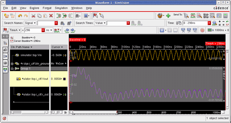
Event-based and Fixed Sampling Time
In the example given in the Low Pass Filter section, the input signal is first converted into a fixed rate sampled data. The filter block is triggered by these events in the always @(Vin) section. This ensures that the filter block is triggered right after the sampling event and a series of filters would trigger one after another in the sequential order.
However, the sampling frequency is a parameter to the filter block itself that is used to calculate the filter coefficients. A mismatch between the actual sampling rate and the filter parameter setting would result in wrong output results. A measurement of the sampling rate inside the filter replacing the instance parameter might be a useful enhancement to overcome this limitation.
The other task would be to change the always block triggering to a time-based trigger, such as always #Ts begin. This would ensure that the filter input is sampled at the right rate and that it is not driven accidentally by a flexible sampling rate. However, the comments above about choosing the right sampling rate still apply.
Furthermore, if a chain of filters triggers at the same time point then the sequence of execution of these filters is unpredictable. Thus, it might be that the sequence of blocks is executed in the wrong order.
Generally, event-based modeling and modeling with fixed sample times are both adequate measures in real value modeling. However, we need to choose the appropriate technique while considering different cases.
ADC/DAC Example
The following is an example of an ADC and a DAC combination. The testbench is creating a different kind of input stimuli including a ramp and a sinusoidal waveform similar to the value sources discussed earlier. In addition, VDD, VSS, and a CLK value are created.
`timescale 1ns/1ps`define Nbits 12`include "constants.vams"`include "disciplines.vams"
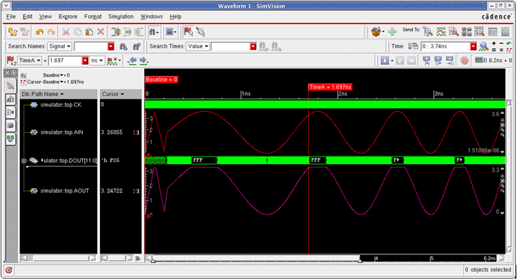
module top ();wreal AIN, AOUT, VDD, VSS;wire [`Nbits-1:0] DOUT;wrealADC I_ACD (DOUT,AIN,CK,VDD,VSS);wrealDAC I_DAC (AOUT,DOUT,CK,VDD,VSS);
real r_ain, r_vdd, r_vss; // input voltagereal Freq=600K,Phase=0; // sinusoid paramsreg clk;
initial begin clk = 0; r_vdd = 3.3; r_vss = 0.0; r_ain=0.1; // out=0.1 for DC op point repeat (10) #10 r_ain=r_ain+0.348; // increasing ramp repeat (10) #10 r_ain=r_ain-0.339; // falling ramp #30 while ($abstime<6000p) begin // generate ramped sine input #2 Freq=Freq*1.0007; // gradual freq increase Phase=Phase+2n*Freq; // integrate freq to get phase if (Phase>1) Phase=Phase-1; // wraparound per cycle r_ain=1.8*(1+sin(`M_TWO_PI*Phase)); // sinusoidal waveform shape end #200 $finish; // done with testend
always #2 clk = ~clk;
assign AIN = r_ain;assign CK = clk;assign VDD = r_vdd;assign VSS = r_vss;
endmodule
The wreal input signals are passed to an ADC block. The first always block calculates the lower and upper limits for the output values and the input value precision (PerBit) given by the input value swing and the number of output bits. These values are updated, whenever the supply values are changing.
The second always block is triggered on every change of the clock. If the input value does not exceed the lower or upper limits, the value is divided by the PerBit value providing the output value in the integer format. This value is assigned to the output bus after a given delay.
module wrealADC (DOUT,AIN,CK,VDD,VSS); output [`Nbits-1:0] DOUT; input CK; input AIN,VDD,VSS; wreal AIN,VDD,VSS; parameter Td=1n; real PerBit, VL, VH; integer Dval; always begin // get dV per bit wrt supply PerBit = (VDD-VSS) / ((1<<`Nbits)-1); VL = VSS; VH = VDD; @(VDD,VSS); // update if supply changes end always @(CK) begin if (AIN<VL) Dval = 'b0; else if (AIN>VH) Dval = {`Nbits{1'b1}}; else Dval = (AIN-VSS)/PerBit; end assign #(Td/1n) DOUT = Dval;endmodule // wrealADC
The inverse digital to analog (or wreal in this case) operation is even simpler. The first always block is almost identical and the second just multiplies the output precision value with the input value bus. The resulting value is assigned to the wreal output wire.
module wrealDAC (AOUT,DIN,CK,VDD,VSS); input [`Nbits-1:0] DIN; input CK,VDD,VSS; output AOUT; wreal AOUT,VDD,VSS; parameter real Td=1n; real PerBit,Aval; always begin // get dV per bit wrt supply PerBit = (VDD-VSS) / ((1<<`Nbits)-1); @(VDD,VSS); // update if supply changes end always @(CK) Aval <= VSS + PerBit*DIN; assign #(Td/1n) AOUT = Aval;endmodule // wrealDAC
The following figure shows the simulation results for the above test case.