11
Extracting Parasitic Resistance (PRE)
Introduction
What Is Parasitic Resistance Extraction?
The Parasitic Resistance Extraction (PRE) capability lets you convert one or more interconnect layers to a resistance-capacitance network. You do not have to perform any preprocessing to prepare the interconnect layers for extraction, as would be the case if you were extracting devices using the extractDevice and extractMOS commands.
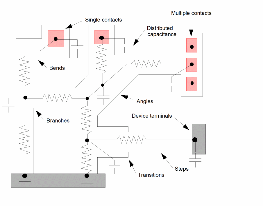
Resistance extraction provides you with a reasonably accurate representation of the interconnect parasitics without incurring excessive processing overhead. Accuracy is obtained by a thorough topological analysis and by inclusion of factors such as bend resistance, transition resistance, and contact resistance, and through the handling of complex shapes, all angles, and multiple terminations to contacts and device terminals.
Distributed capacitance of the interconnect can be included in the extraction with your own choice of the resistance-capacitance (RC) model as well as the various coefficients and factors.
How Do I Invoke It?
Resistance extraction is triggered through the measureResistance command, which must precede the last geomConnect command in the rule deck. Resistance extraction is performed as part of a normal layout extraction run in which the circuit network is extracted from the layout and stored in an extracted view of the circuit.
What Are the Results?
During circuit extraction processing without parasitic resistance, an extracted view of the circuit is produced in which every electrical net formed by the layout is represented as a single entity in the data.
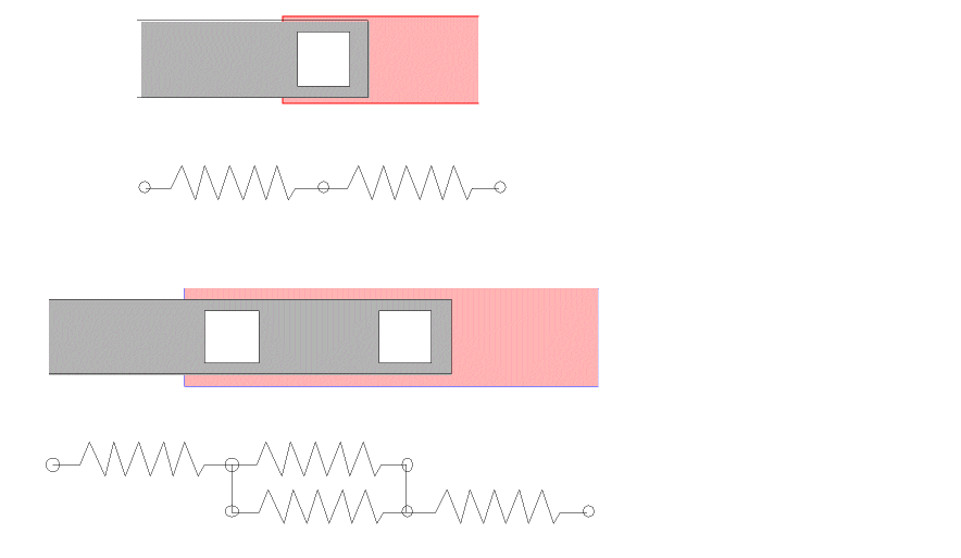
Parasitic resistance works on one connected layer at a time. Any part of an electrical net that is composed of the specified layer is broken down into a resistor-capacitor network. The parts of the net that are not composed of resistance layers are left as before.
The result is that each single entity that is an original net becomes a network. The original net no longer exists. If the original net was labelled, the part of the original net that overlaps the label uses that label for the net name. The additional nets created have names based on the original net name and a sequence number. You can control the exact format of the name used for the additional nets by defining the SKILL procedure ivUserNetNameFormatter. If the SKILL procedure is not defined, Diva uses a default format of <original-name>:<sequence-number>. An example of the Skill procedure that mimics the default behavior is:
procedure( ivUserNetNameFormatter( name number )
   get_string( concat( name ":" number ) )
); end iVUserNetNameFormatter
The original devices which were recognized by the extractDevice and extractMOS commands are unchanged. New devices representing the resistors and capacitors are added.
The layers used for resistance extraction are removed from the circuit to form the resistors themselves. Therefore, they are no longer available for other parasitic measurements, such as cross-coupling capacitance.
The Extraction Process
Several separate operations are performed during parasitic resistance extraction. Processing is split into two sections.
- The first section is performed before the circuit interconnect extraction and is the preparation of the data. It is performed for each layer defined to be used for resistance extraction.
- The second section is performed after the interconnect extraction and is the actual recognition and measurement of resistors and capacitors.
Preconnect
The resistance layer is split into two separate layers. The first layer is a replacement for the original interconnect layer and consists of the areas formed by the contacts and pins plus special areas formed from device recognition shapes see the “Device Terminals”. This layer forms the terminals of the resistors. The second layer is all of the original layer minus the terminal layer and forms the shapes to be converted into resistors.
To enable the capability of combining resistance extraction and cross-coupling or fringe capacitance extraction, you can also specify that a special additional layer be derived that consists of a concatenation of the terminal and resistor layer. This layer appears to be almost identical to the original layer but has the correct nodal information to allow parasitic capacitance to be measured. You can use this special layer as input to the parasitic measurement commands.
You can also request that the resistor bodies be fractured into smaller pieces to allow more accurate distribution of the cross-coupling capacitance inside the resistor network.
Postconnect
The resistor layer is processed to extract the resistance and capacitance network it contains. Each contact or device terminal that was cut out to form the resistance layer acts as a terminal to the extracted network. The devices and nets forming the extracted network are added to the extracted view of the circuit, supplementing the devices and interconnect already extracted through device and connectivity extraction steps.
The extraction process consists of breaking the resistor layer down into small pieces. Each piece can have its resistance and capacitance calculated with compensation for bends and transitions. These resistances and capacitances form an initial network into which contact resistance is added. The network output is then reduced to its simplest form.
Each resulting device in the network is an entry that has a resistance value and a capacitance value. You can use the system netlisting capabilities to translate these devices into networks of their own, such as Pi or Tee R-C networks.
Resistor Formation
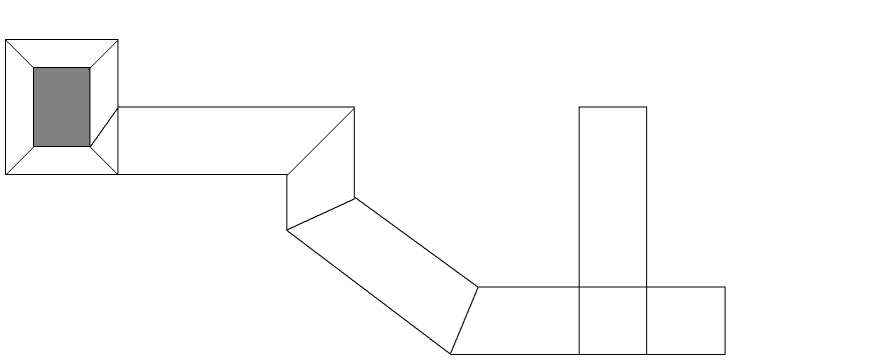
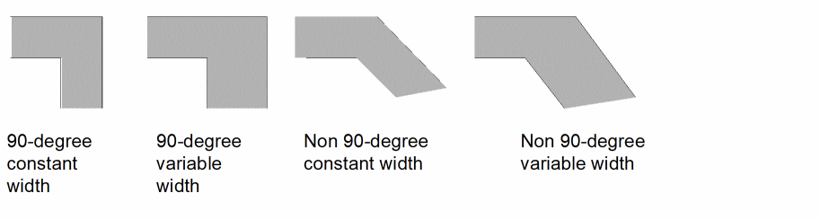
Forming resistors from polygon shapes requires several steps. The individual polygons on the resistor layer are fractured into pieces. Each piece has a maximum of four sides and no external angles less than 180 degrees (the piece has no reentrant angles). Each piece has its edges identified as external edges of the original shape, as connections to other polygon pieces, or as connections to contacts and device terminals. This concept is illustrated for a simple polygon. Complex polygons follow the same process.
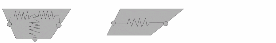
Each polygon piece has possible current flow between all contact edges, terminal edges, and connections to other pieces. For each possible current flow path, the shape is analyzed and the resistance of that path is calculated. All the resistance paths are then combined to form a network. There can be from zero to four resistors in each polygon piece. As far as current flow is concerned, the pieces with zero resistors are dead ends. The following figure illustrates examples of resistance networks inside polygon pieces.
The determination of resistance for each path in a polygon piece includes compensation for bends, steps, and transitions. Even though each individual piece does not have these configurations, the information from the original polygon, necessary for the calculations, can be deduced from the pieces.
During the fracturing process, the external edge length and area of each polygon piece is measured and associated with the piece. If you supply a calculation as part of the resistance extraction command, the capacitance of each polygon piece is calculated and distributed among the resistors calculated from the piece.
Contact Resistance
The program considers three components of contact resistance during the resistance network extraction.
- The resistance relative to current flow around the contact
- The resistance of contact edges
- The resistance of contact area
Current Flow
You conventionally apply a compensating factor to the resistance along a net based on the width of the contact to that net and the width of the net itself. This approximation is intended to compensate for the change in resistance created by current flow around the contact.
This program’s resistance extraction methodology makes contact compensation unnecessary since it extracts the complete network around the contact.
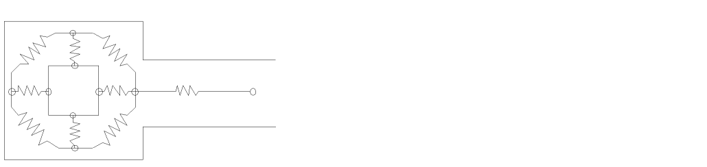
The following figure illustrates an example of a resistance network around a single contact. This form of network extraction is applied in all contact configurations, whether there be single, multiple, or arrays of contacts.
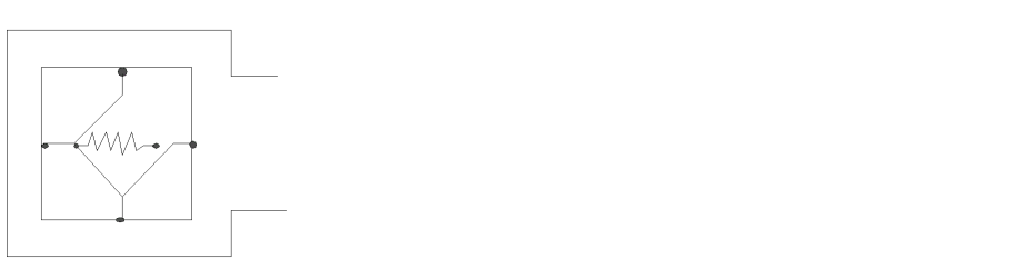
Edge Resistance
Contact edge resistance is considered when current is flowing across the edge from the net to the contact or vice-versa.
You conventionally consider only the edge of the contact that is perpendicular to the main direction of the net to which it connects. This is an approximation because you have no information as to the current flow around the contact.
Since the program does have the current flow information around the contact in the form of the extracted network, it can utilize the resistance of all edges of the contact. The program therefore measures the length of each contact edge and applies to it the coefficient you supplied for contact edge resistance with the assumption that the resistance value of an edge is inversely proportional to its length.
You can define a different edge resistance coefficient for each type of contact.
The following figure illustrates the edge resistance of a contact in isolation from other resistances.
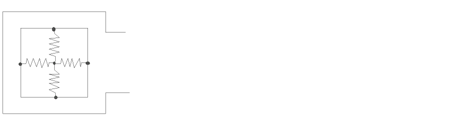
Area Resistance
Resistance of the contact area is considered as a resistance to the flow of current through the contact. The coefficient you supply is used to calculate the resistance inversely proportional to the contact area.
You can define a different area resistance coefficient for each different type of contact.
The following figure illustrates area resistance of a contact in isolation from other resistances.
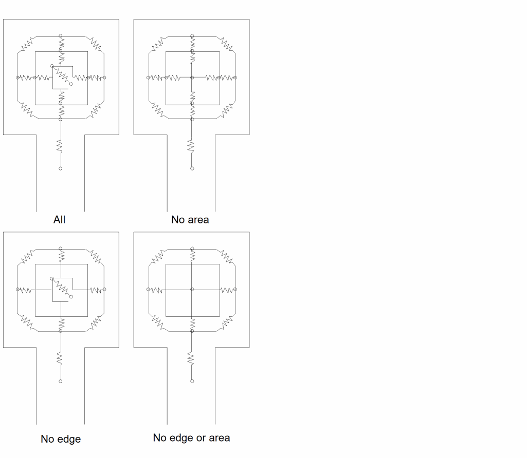
Since the contact edge and area resistance extraction capabilities are both optional, the network output can be formed in one of four ways, as illustrated in this figure.
In all cases, the resistors on the side of the contact away from the current flow direction have little effect on the total resistance, but they do accurately model the true circuit.
Device Terminals
Connections to resistors are formed from contacts, pins, and device terminals formed from the device recognition shapes. For pin and contact connections to resistors, Diva uses the complete area of the connection shape as the connection to the resistor. For device terminals, Diva has to create special connection shapes using the device recognition shape as the base.
There are two types of device terminals. A resistor shape can butt against a device recognition shape to form a terminal as in the source/drain of an MOS transistor. A resistor shape can also pass across a device recognition shape to form a terminal as in the gate of an MOS transistor.
To form connectivity for the device terminal recognition, each device terminal has to be represented by a shape on the interconnect layer. If Diva converted all the interconnect layer to resistor layer there would be no terminals left for connectivity, so Diva creates its own terminals.
For the source/drain type of connection, Diva creates a terminal at each butting interface between the resistor layer and the device recognition shape.This terminal is a narrow sliver along the butting edges. Its existence lets Diva recognize both the resistor and device terminals.
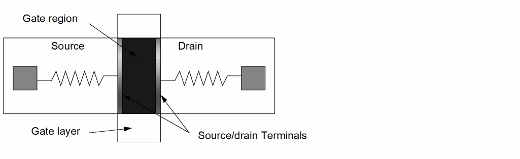
For the gate connection, Diva creates a very narrow sliver across the device between the source and drain edges. This sliver has area, so it behaves as a normal terminal to the device during device extraction. However it is small enough that is has virtually no effect on the resistance along the path through the gate.
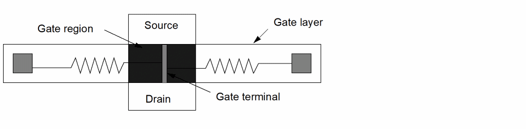
For both these connection types, the final interconnect layer has no shape that represents the full device recognition shape. This means you cannot use the original resistor layer to make device parameter measurements. For example, if you convert gate polysilicon into resistors you cannot measure gate width by measuring the length of polysilicon coincident with the gate region. You must measure the length of the gate region butting the source/drain layer.
If there is a contact or pin over the gate region, and the area of that contact or pin does not intersect with the gate sliver terminal, the gate has two connections and is flagged as badly formed.
Bend Resistance
You can provide a bend resistance factor to the program so that it can more accurately calculate the effect of bends in a path on the resistance of that path. You provide a factor that is defined for right-angled bends where the path width does not change from one side of the bend to the other. For bends in which the paths on either side of the bend are of different width, the factor is modified to cover the angle of the bend plus the transition effect from one path width to another.
If you want a 90-degree bend to be considered as if the current always flows through the center line, you would have to provide a factor of 1. The default factor applied by the program if you do not provide one is 0.56. For bends other than 90 degrees, the program uses a portion of the factor you supply based on the angle between the paths on either side of the bend. The smaller the angle, the smaller the factor used.
The following figure illustrates sample bend configurations for which the program compensates.
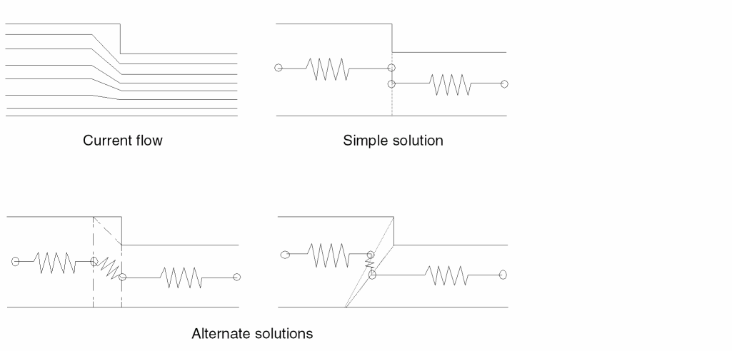
Transition Resistance
A transition is a sudden change in the width of a conducting path. Generally, the term transition is used when the one or both sides of a path form a step. In the examples, the discussion is limited to a step on a single side, but the principle applies in both cases.
The transition effect on current flow is to form a dead corner through which no current actually passes. Since all the resistive material of the path is not in use, the resistance formed by the path is higher than would be the case if all the material were used.
The figure shows the current flow pattern and examples of how the resistance could be calculated.
The simple solution does not consider the transition, and results in a calculated resistance value higher than the real value. The alternate solutions show how the program methodology of cutting the original shape ensures that the calculated resistance is as close to the real resistance as possible. The appropriate shape cutting is automatic, requiring no user information or intervention.
Network Reduction
The resistance extraction process described so far results in a large number of individual resistors connected in a complex network. Even a simple “dog-bone” resistor can result in over 36 resistors representing a single resistance path. Although this is an accurate representation of the resistive circuit in the original shapes, it would consume an unacceptable amount of storage space and be time-consuming to simulate.
To overcome this, the program reduces the network to a minimum configuration. A dog-bone shape should reduce to a single resistor. The reduction process uses a series of transformations in an iterative sequence. Each sequence reduces the number of resistors. The program repeats the process until no more reduction takes place.
The reduction process does not reduce the accuracy of the network. The transformations used give exact equivalent circuits. No approximations are made.
In most cases, the reduced network includes the minimum number of resistors required to represent the circuit. For some circuits, the program might produce a less-than-minimum result when the network reaches a configuration that cannot be reduced further by the tools available.
The resistor configuration produced by the program might not match your concept of what that configuration should be. The result, however, is meaningful and accurate.
You can also eliminate resistors from the network after the reduction process completes by using the ignore option. The ignore option replaces resistors below the value you define with short circuits and replaces resistors above the value you define with open circuits.
Cross Coupling and Fringe Capacitance
Measurement
You can specify an output layer for the measureResistance command. This layer is the original layer you defined for resistance but contains separate polygons for the resistor bodies and contacts, pins, and device recognition polygons that form the terminals of the resistors. It is a composite of the resistor layer and the remaining interconnect layer.
You treat the output layer like any other derived layer containing unmerged data. For most situations, Diva treats the layer as unconnected. However, you can use the layer to measure parasitic capacitance with the following commands:
In these cases, the language parser treats the resistance output layer as if it is connected. You use the layer in these commands just like any other connected layer.
The output layer from measureResistance must not be used with the complexParasitic command. This new command requires the input layer of measureResistance to be used. The complexParasitic command will automatically locate any measureResistance command which processes the layer, and cause measureResistance to produce the data needed by complexParasitic.
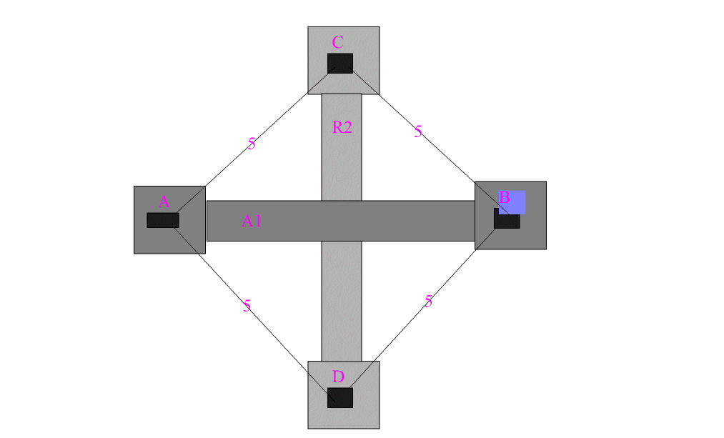
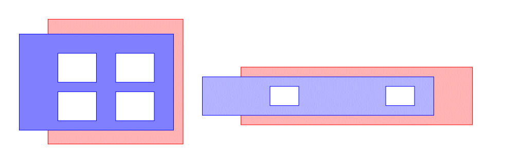
Any parasitic measurements made between the resistance output layer and any other layers are evenly distributed to the terminal connections of the resistors. For example, in the following figure
- The resistor connected between terminals A and B.
- The resistor crosses net C with a cross coupling capacitance of 10.
-
Two capacitors are formed:
A to C = 5 B to C = 5
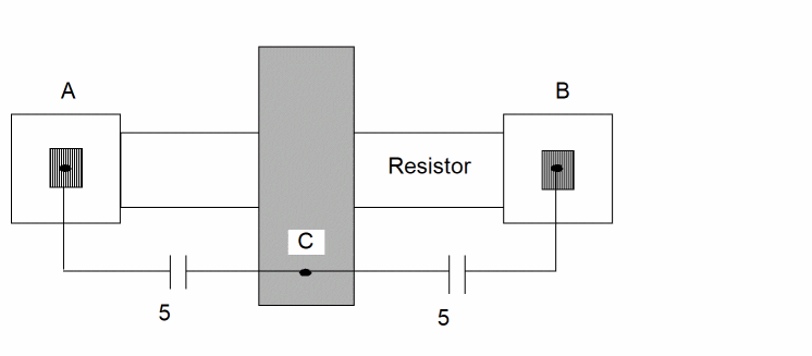
Any capacitance to nets directly connected to the resistor body are considered as capacitors to the same net and are ignored.
Measurements can be made between two or more resistor bodies, and the resultant values are distributed between all the resultant terminals. For example, in the following illustration
- Resistor 1 (R1) is between nets A and B
- Resistor 2 (R2) is between nets C and D
- The value of 20 is measured by R1 crossing R2.
-
These capacitors are formed:
A to C = 5 A to D = 5 B to C = 5 B to D = 5
You can manipulate parasitic measurements made from a resistor body like any other measurement by using the calculateParasitic and saveParasitic commands.
When using measureFringe on resistor bodies, it is recommended that you always use the shielded and opposite options in the drc command. This is recommended whenever you use measureFringe, but is even more important when you use the command on resistor bodies because the layer you are measuring consists of the concatenation of the resistor bodies and the resistor terminals. This concatenation results in internal edges at the interface between the two layers. If your resistance layer originally terminated at a gate (like the source/drain of an MOS device), this butting edge is included in the parasitic measurements and might cause false capacitance values.
If any resistor shape has no terminals, it is not included in the parasitic measurements because there are no terminal nodes to which the resultant capacitors can attach.
Distribution
For resistors or networks derived from larger polygons, the even distribution of capacitance on the original resistor terminals might be inaccurate. To improve the accuracy, you can fracture the original resistor bodies into smaller pieces. You can provide a command line option to control the size of these pieces.
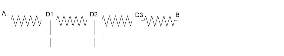
Diva fractures resistor bodies for better distribution of resistance and capacitance by creating extra terminals along the path of the resistor. These extremely narrow terminals cut across the resistance path and have little impact on resistance and capacitance calculations. When you measure cross-coupling capacitance on resistors where fracturing has been applied, separate measurements are made for each fractured resistor piece and are distributed only to the terminals of that piece. Consider the following example:
A path has been cut into four pieces and has a cross coupling-capacitance across the second piece. The original terminals of the shape are A and B. The extra terminals created by the distributed cutting are D1, D2, and D3.
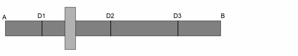
The resultant network shows the cross-coupling capacitance value distributed only to the terminals of the second piece.
The fracturing applies to all resistor body shapes, but the actual cuts are made only in parallel-edged horizontal and vertical sections of the resistor. The extra terminals are narrow and have a minor effect on the resistance and capacitance values. For example, a resistance of 10 might become 9.99.
Diva has been designed to provide consistent results when fracturing shapes that you place at different orientations. However, it is possible that in some circumstances rotated shapes are cut differently.
Diva maintains the length of the fractured segments in a straight, parallel-edged path, close to the distribution factor you provide. However, no attempt is made to maintain the exact length of segments that form steps, bends, or branches.
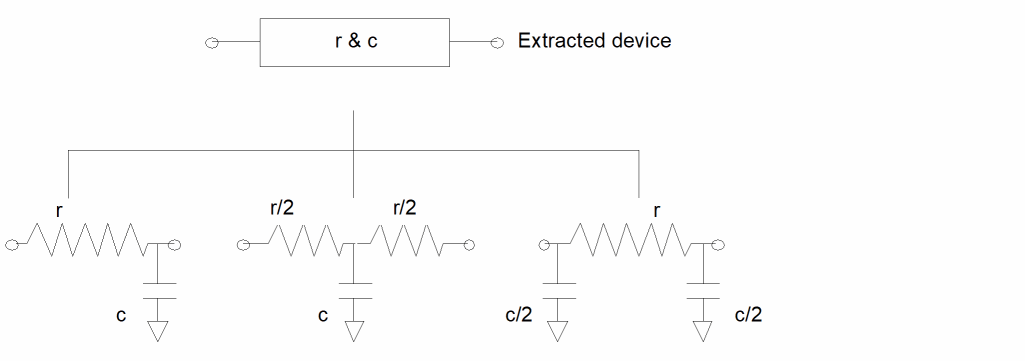
Resistor Body Capacitance
As described under Resistor Formation, during the creation of the resistor pieces from the original shape, the area and external edge length of the pieces is used to calculate a capacitance value for those pieces. The area is the complete area of the piece, and the edge length is the length of any edges of the piece which were also edges (or partial edges) from the original shape. These values are used in the calculation you supplied in the original measureResistance command to generate a capacitance value for the piece.
When the resistor network is calculated for each piece, that capacitance value is distributed among those resistors. During the resistor network reduction phase of this verification, the capacitance values are consolidated along with the resistors. The result is a single value of capacitance associated with each resistor in the reduced network. As with the resistance values, no accuracy is lost during the reduction process.
R-C Models
Although this description of the resistance extraction process has, up to now, used the word resistor to describe the devices extracted by the program, this is not exactly true. What has been extracted is two terminal devices of undefined type that have both a resistance value and capacitance value. It is up to you to give these devices a model name and to provide a device library element for them.
For the purposes of netlisting these devices, you can either set up the netlist control to have each of your own device types generate a netlist entry directly, or you can have each device be represented by a schematic containing a subnetwork that forms a netlist down to individual resistors and capacitors. Within this subnetwork, you can choose the required resistor and capacitor network formation.
Netlisting R-C Models
The major difference between normal netlisting R-C models and normal netlist control is that the properties containing the values of resistance and capacitance are not on the instances of the resistors and capacitors, but on the instance of the higher level cell.
Each lower level device in the schematic can have associated with it only a portion of the value assigned to that property on the instance of the cell. For example, if the property value on the cell for capacitance is 20, and the schematic cellview of it contains two capacitors, each capacitor needs to have a value of 10 generated for it in the netlist.
To facilitate netlisting for this situation, the following procedure must be adopted.
- Create a cell called pirescap for the device to be extracted from the resistance program.
-
This cell needs two cellviews, one called symbol containing a picture of the circuit used to display the device in the extracted cellview, and one called schematic containing interconnected instances of resistors and capacitors, which is used by the netlister. The resistance extraction program creates instances of this cell and adds two properties to each. For example
r = 12.65 c = 134.9 -
The pirescap schematic cellview contains a circuit consisting of a single resistor with a capacitor to ground at either end. The single resistor is an instance of a device called pires and the two capacitors are instances of devices called picap. Both devices have cellviews called “lvs” with similar properties. The capacitor is used in this example.
NLPModelPreamble = [@NLPcapacitorModelCard] NLPElementPostamble = [@NLPElementComment:%][@NLPcapacitorElementCard] LVScapacitorProp = resPrintCBy2( ) -
The first two entries have the type of NlpExpr and are the same as those on a normal capacitor. The third entry defining the property has the type of ilExpr. The Postamble entry references the capacitor element entry which is in the nlpglobals cellview. The capacitor element entry references the property entry. Normally, the property entry is found in nlpglobals, but in this case, the one shown in the capacitor itself takes precedence. The property entry references a SKILL procedure that must be provided by the user.
procedure( resPrintCBy2( )
   prog(( str tmp )
      tmp = fnlSearchPropString( "c" nil )
      if (tmp, then
         tmp = evalstring( tmp ) / 2.0
      else
         tmp = 0.0
      )
      sprintf( str "\ c %f " tmp )
      return( str )
   )
)
The fnlSearchPropString procedure searches through the hierarchy leading to the device instance, looking for a property called c. In this case, it finds it on the parent instance of the capacitor, namely, the instance of pirescap. The value is returned as a string and is converted to a number by the evalstring procedure and divided by 2.
The resultant value is then printed into a string along with the remaining text required by the final property (in this case, the enclosing quotes and the c character) and returned, which has the effect of printing it in the netlist. In the example, a similar routine is needed for the resistance, but without dividing its value by 2.
The resistance extraction program is working with devices that have two terminals. The only additional nets that can be introduced into the schematic are global signals such as power and ground.
Multiple Layer Extraction
Your run command stream can have more than one resistance extraction command. Each command applies to a different interconnection layer, and there are no interactions between the devices created from one command and the devices created from another.
Since the extraction and reduction process works on a shape-by-shape basis, the terminations of each shape (the contacts and device terminals) remain the terminations of the network generated for that shape. For example, a single interconnection line formed from two layers joined by a single contact causes two resistors to be created, one for each layer, with a junction net at the contact between them. The circuit reduction does not proceed across that contact.
Unexpected Results
There is one situation that causes unexpected results if you are not careful. As explained, if you request extraction of two or more layers, and any two of them are directly connected by a contact, the network reduction is broken at that point. The manner in which the contact is cut from the resistor prior to resistance extraction creates a new electrical net at the contact area.
If the connection between the two layers is made at any point by multiple contacts, each contact area becomes a separate electrical net. Since they are independent nets, resistance extraction causes discrete resistors to be created between them. This can be seen in the figure, which shows how a single contact between two resistance layers causes a break in the network, and how two contacts result in a more complex network.
As the number of individual contacts forming a single connection between two resistance layers increases, so does the complexity of the network. The lowest number of resistors between three contacts is three on each layer, totalling six. The lowest number of resistors between five contacts is ten on each layer, totalling twenty. As the numbers of resistors increases, the problems of subsequently processing those devices increases.
You reach a point where you won’t want such a network formed. There are techniques you can use to overcome the problem. The results are not quite as accurate as having the full network, but the degradation is minimal.
The paragraphs detail two techniques to handle the problem. Both rely on the same principle but approach it in different ways. Each has its advantages and disadvantages. Both cause all the contacts at a single connection to be connected to a single net, allowing better network reduction.
A Simple Approach
The simplest way to make all contacts at a single point have a common net is to generate a new layer from the intersection of the two resistance layers and include it in the connect command.
short = geomAnd( metal1 metal2 )
measureResistance( metal1 "resistor" 1.0 "r" )
measureResistance( metal2 "resistor" 1.0 "r" )
geomConnect ( via( via short metal1 metal2) )
In this example, a layer called short is created as the and of metal1 and metal2. During the preparation for resistance extraction, the metal1 and metal2 layers is split into the areas wanted for resistance, and the areas under the contacts. During the connection process, if there are no contacts over a shape on the short layer, no connections are made. Where there are contacts over a short shape, the remaining contact areas of metal1 and metal2 connect as normal, and each area connects to the same short shape, forming a single electrical net.
This figure shows two examples of multiple contacts. The first figure illustrates a case where the approach gives a reasonable result. The second figure, however, illustrates a case where the result becomes significantly inaccurate. There is a large resistance between the contacts which disappears if the contact areas are on the same electrical net.
A Better Approach to get More Accurate Results
This approach requires more commands and absorbs more processing time, but provides more accurate results.
close = drc( via sep < 3 opposite )
short = geomOr( via close )
measureResistance( metal1 "resistor" 1.0 "r" )
measureResistance( metal2 "resistor" 1.0 "r" )
geomConnect( via( via short metal1 metal2 ) )
The drc command creates shapes from the areas between close contacts. The value used for the separation depends upon your own understanding of the technology and definition of when contacts can be considered common and when they cannot. The shape results are then combined with the contacts themselves to produce the same short layer as in the previous example, which is then processed the same way in the connect command. In the previous figure, the first figure shows contacts shorted together (providing they are closer than the drc separation value). The second figure shows contacts remaining separated with the network resistor result between them.
Using Shorts to Reduce Large Contact Array Resistor Networks
You must grow and shrink the contacts by an amount sufficient to merge contact arrays and then use the resultant layer as the "short" layer. This has the effect of giving all contacts in the array a common node, but it does not bypass the measurement of the network around the node or the contact resistance measurement. The program will still need time to create the network inside the contact array, but the time to reduce the network down is significantly reduced and the resultant network is much simpler.
This provides an intermediate solution between leaving the contacts as they are (which is expensive in run time and creates a very large resistor network) and growing and shrinking the contacts themselves which eliminates the contact resistance accuracy.
Command Reference
The following section discusses the measureResistance command.
measureResistance
[outlayer=] measureResistance( reslayer model rescoeff [bf] resprop [cap] [ignore] [save][contact][distribute][capLimit]
[namePrefix(string)][property(name value) ...])
Description
The measureResistance command extracts a resistance-capacitance network from an interconnect layer. The extraction process allows for sheet resistance, bend resistance, transition resistance, terminal resistance, contact area resistance, contact edge resistance, area capacitance, edge capacitance, and user defined R-C models.
Prerequisites
The layer to be processed for resistance extraction must be referenced in a geomConnect command. The measureResistance command must precede the geomConnect command.
Fields
An optional output layer consisting of the original resLayer separated out into the resistor bodies and the resistor terminals (cuts, pins, gates, and device recognition shapes).
If you specify this option, you can treat the outLayer as any other unconnected derived layer, except that it is unmerged. For the purposes of parasitic extraction, you can treat it as a connected layer, except for the complexParasitic command, which must be given the reslayer.
The following parasitic measurement commands accept the outLayer as a connected layer:
measureFringe multiLevelParasitic
Any parasitic capacitance created with a shape on the resistor output layer is distributed evenly between the terminal nets of the resistor network extracted from the shape.
If you do not specify this argument, no output layer is created.
The layer to be processed for resistance extraction. This must be a derived layer used in a geomConnect command. The layer is used for both input and output. On input, the layer is the originally derived interconnect layer. The resistance extraction process removes those areas of the layer which becomes resistors, leaving only those areas which form contacts and device terminals. It is these remaining areas which compose the output layer.
The area of the input layer that forms the resistor bodies can be saved separately, if required for reference, using the save option of the measureResistance command.
The device model name consisting of a character string enclosed in quotes. The model can represent a low-level device such as a resistor or a higher level device that netlists down into a resistor and capacitor network.
The character string must define the model name and the view name. If the view name is omitted, the name symbol is defaulted. The defined model must be available in a library accessible to the program so that the terminal configurations can be verified and instances of the device can be placed in the extracted view of the circuit.
The defined model must be a two-terminal device in which the terminals are interchangeable (nonpolarized). Because of this, the terminal names are not required to be specified in this model definition since they can be deduced directly from the model.
A floating point or integer value representing the resistivity of the interconnect layer being processed, in ohms per square.
An optional bend factor for adjusting the values of resistors having bends. The value is the resistance in squares around a single 90-degree bend, replacing the theoretical measured value of 1.
The bend factor is automatically adjusted for bends having angles other than 90 degrees and for bends whose legs are of different width. The bend factor is also applied to step transitions between one width and another in straight resistors to improve the accuracy of resistance calculation.
If you do not provide a bend factor, the program defaults to a 0.56 value.
The name of the property to be attached to the device to contain the value of its resistance. This must be a text string enclosed in quotes.
An optional argument to specify the parameters for capacitance measurement. If not defined, no capacitance extraction is performed. The options are
This is a keyword introducing the capacitance definition.
The name of the property to be attached to the device to contain the value of its capacitance. This must be a text string enclosed in quotes.
This equation converts the area and perimeter of the capacitor into a single capacitance value. It uses the symbols a (area) and p (perimeter). No other symbol is allowed in the equation. The full range of procedures used in the calculateParasitic and measureFringe commands are available.
Since the capacitance calculation is performed on resistor pieces, and the perimeter measured is from the original shape’s external edge perimeter, it’s possible that some resistor pieces have no original edge perimeter, resulting in a p value of zero. Do not perform a division using the p symbol.
Here is an example of the cap option.
cap( "c" 0.35 * a + 1.02 * p )
This optional argument lets you remove resistors from the circuit if their values fall outside the limits you specify.
This argument has the following syntax:
Any positive integer or floating point value.
One of the following operators:
For example, the following syntax removes all resistors whose value is less than 1.
The following example removes all resistors whose value is greater than 1,000.
The following example removes all resistors whose value is less than 1 and more than 1,000.
Any resistor that is removed because its value is lower than the limit you specify is replaced by a short circuit. Any resistor that is removed because its value is greater than the limit you specify is replaced by an open circuit.
You cannot specify a range of limits using the ignore keyword. For example, the following syntax is invalid:
Any capacitance associated with the removed resistors is distributed around the resistors on the resultant nets.
keep or ignore options. A resistor was never removed, regardless of its value, if one of its nets was connected to a contact, device terminal, or pin on the original net. This was true even if the value of the resistor would otherwise cause it to be ignored.
In the 4.4.3 release and all subsequent releases, resistors can now be removed based on their values regardless of their connectivity.
The program automatically ignores very small resistors during network reduction, whether you specify the ignore option or not. The program applies the ignore option after the network reduction.
This optional argument allows you to save the shapes representing the resistor bodies in the extracted cellview.
This is a keyword introducing the save layer definition.
The name of the graphics layer, in quotes, on which the resistor body shapes are to be stored.
This is a keyword that creates fracturing lines, which lets you see how the geometry is cut up before analysis.
This is an example of a save option.
The shapes saved on this layer are for display purposes only. They are not associated with the electrical network in any way. They are a subset of the original connectivity layer used to create the resistors. The remaining shapes from the connectivity layer remain on that layer and can be viewed by saving the connectivity layer in the normal way.
This optional argument lets you specify parameters for contact resistance measurement. Without this argument, no contact resistance is measured. Any number of these arguments can be specified for different contact and terminal layers. The same process is applied to contacts and device terminals.
contact( layer acoeff lcoeff )
Keyword introducing the contact resistance definition.
The layer reference for which the contact resistance is to be measured. The layer must appear in a geomConnect command.
A floating point or integer value that defines the coefficient to be applied to the contact to convert its area into a single resistance value in the resultant network. The resultant value becomes inversely proportional to the area. If this coefficient is not required, its value must be set to 0.0.
A floating point or integer value that defines the coefficient to be applied to the contact to convert its edge lengths into individual resistors in the resultant network. Each edge forms a resistor between the contact and the surrounding interconnect, whose value is inversely proportional to the edge length. If this coefficient is not required, its value must be set to 0.0.
This optional argument lets you limit the number of terminals used when distributing parasitic capacitance values created between a resistor body and another shape.
The required value N is the maximum number of resister network terminals used when distributing parasitic capacitance. The terminals used are selected by the software on a first-come, first-used basis.
The primary purpose of this option is to reduce parasitic capacitance runtimes and disk usage. Improvements in data handling have greatly reduced the impact of large numbers of resistor network terminals. We no longer recommend the use of this option.
This optional argument lets you fracture the resistor bodies into smaller pieces to obtain more accurate resistance and capacitance distribution. The distribute argument has the following form:
The distribute keyword tells Diva to fracture the resistor shapes into smaller pieces.
The optional value N is any integer greater than 1. The value is directly related to the size of the fractured pieces that result. If you specify the distribute keyword but do not specify a number, a default value of 12 is used. If you do not specify a keyword, the resistor bodies are not fractured.
The value of N is allowed to be zero for the special case of disabling the distribute option.
The value N defines the ideal length in squares that each fractured piece should be if a single straight path is fractured. For irregular shapes and branched shapes, there may not be any unbroken paths of this length, but Diva still fractures the shape. The larger the number, the larger the pieces are.
Fracturing introduces new terminals in the circuit. These extremely narrow terminals span the resistor bodies (hence cutting them into pieces) and have virtually no impact on the resultant resistance and capacitance of the pieces. These terminals are positioned only in horizontal or vertical sections of the resistor body.
distribute option in conjunction with the keep or ignore options. The splitting of the resistor bodies into two or more pieces using the distribute option creates new terminals. For purposes of resistor removal, these new terminals are treated as if they were part of the original net. The result is that pieces created by the distribute option cannot be removed, even if the value of the resistor would otherwise cause it to be ignored.
This implies that there can be situations where the entire resistor in a branch is removed when the distribute option is not used, but none of the pieces are removed when the distribute option is used.
This above problem has been fixed in the 4.4.3 release. All resistor pieces created by the distribute option can now be removed based on their values using the keep or ignore options.Optional argument that allows you to specify the character string to use as the prefix for the instance name. Instance names are constructed from the prefix and an integer value to create a unique name. If not provided, the default prefix of “+” is used.
The string parameter must be quoted string or an expression that evaluates to a string.
Optional argument that allows you to specify a property to be attached to each instance generated by the measureResistance rule. More than one property option can be used in a measureResistance rule.
The name parameter must be a quoted string or an expression that evaluates to a string.
The value parameter must be a quoted string, integer constant, real constant, or an expression that evaluates to a string, integer or real.
Examples
Since the number of permutations of this command is large, these examples illustrate one minimal command and one using all options.
measureResistance( poly "resistor" 30.5 "r" )
measureResistance( metal "res_pi_cap" 30.5 0.5 "r"
   cap( "c" 1.5e-12 * a + 2.7e-13 * p )
   ignore <= 0.15
   save( "resist_body" )
   contact( cut 0.1 2.5 )
   contact( via 0.08 1.4 )
   distribute( 20 )
)
Return to top