13
Comparing Layout to Schematic (LVS)
Introduction
The Layout Versus Schematic (LVS) program compares two versions of a circuit and isolates any differences. You can use it to compare two layouts, two schematics, or a layout and a schematic.
- Generates a netlist for each representation of the circuit.
- Compares the circuit versions using the verification rules commands you enter in the LVS rules file and the run options you specify from the menu.
- Compares device parameters using an internal feature that combines parameters during series and parallel reduction.
- Lets you provide correspondence points to improve error isolation. Correspondence points identify equivalent devices or nets in each representation of the circuit.
- Outputs error files that can be used to view and probe errors.
- Displays and explains the errors it found.
The LVS program is controlled by the system simulation environment (se). The simulation environment is set up by your system administrator and normally you do not need to know about it. However, to compare symbolic cellviews or macro cells, you must alter the environment defaults. See
You can run LVS using the LVS command from the Verify menu or using the ivLVS SKILL function. You can also run LVS in the UNIX environment.
The LVS comparison algorithm uses a combination of “signature analysis” and “circuit tracing” algorithms to provide the best possible matching of the two circuits with minimum additional input from users. However, there are situations where the circuits are ambiguous and the normal processing cannot clearly identify the matching. In these situations, users can introduce the device parameters into the algorithm to act as a “tie-breaker.” For more information, see the “Parameter Analysis” section and the parameterMatchDegree function description in this chapter.
Prerequisites
The prerequisites for LVS are as follows:
- You must define LVS verification rules in a text file.
-
You must extract networks for both cellviews so that LVS can generate the netlists it needs.
To create the layout network, run an extraction on the layout using the Extract command from the Verify menu to get an extracted view.Sometimes the extracted view contains devices, such as parasitic devices, that you do not want to include in the netlist for LVS checking. For any devices that you do not want to include in the netlist, you must set the lvs view property nlAction to ignore. The nlAction property must be placed in the property list of the device’s cellview.To create the schematic network, run a check on the schematic using Edit – Check – Current Cellview. - You must initiate LVS from a window containing either a schematic cellview or an extracted layout cellview.
Capabilities
You control LVS processing by entering verification rules commands in LVS rule file and by choosing options in the LVS form, which you access by selecting the LVS command from the Verify menu. The verification rules commands define the type of verification checks you want to run. The LVS form options define requirements for a specific run.
The verification rules commands can do the following:
- Permute (interchange or combine) devices
- Ignore device terminals
- Ignore extraneous devices
- Analyze parameters
The LVS form offers the following options:
Additional capabilities are as follows:
Backannotation
You can backannotate the names of the nets and instances in the schematic view of a circuit to the extracted view of the circuit after LVS runs.
You can perform backannotation by executing the Diva verification lvsbx stand-alone in the UNIX environment. This function is described in some detail at the end of this chapter.
Verification Rules Functions
This section discusses the functions performed by the LVS verification rules commands. You can find the syntax for these commands at the end of this chapter.
Permutating Devices
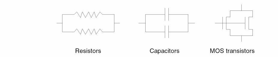
The permuteDevice command lets you reduce (combine) all devices of the same type to a single device. This command lets you reduce series, parallel, and MOS devices, and define functions which combine the device parameters during this reduction process.
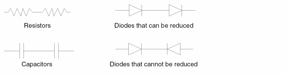
Permutation eliminates physical differences where the physical differences have no effect on the functional equivalence of the circuits. Simple examples of this are the reduction of series and parallel devices into single devices, and the pin permutability of MOS transistor sources and drains.
If a terminal name exists in both cellviews, devices cannot be permutated across that terminal. No series, parallel, or MOS permutation absorbs a terminal.
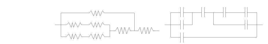
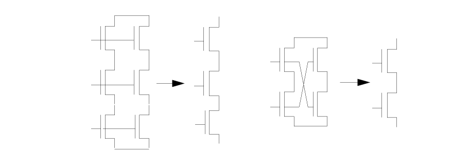
Series Reduction
You can combine devices of the same type that are connected in series by using “series reduction.” To combine in series, your device type must have two terminals, be a MOS device, or have a three-terminal resistor configuration.
For two terminal devices the two devices must be connected by a single net. That net must not be connected to any other device and must connect one of the terminals from each of the devices being combined. If the two terminals of the device type are permutable, it doesn’t matter which two are connected. If the two terminals of the device type are not permutable, then the connection must be between unlike terminals.
The following figure illustrates typical series configurations.
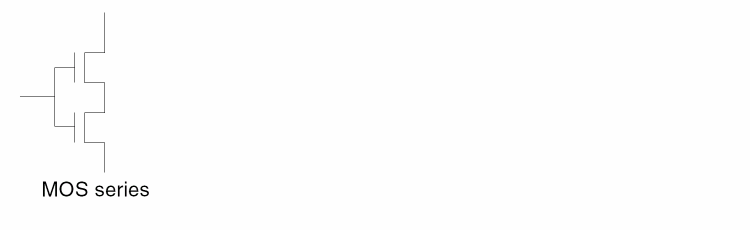
For MOS devices to be combined in series, they must share a common gate and a common source or drain region.
You can specify three terminal resistors and capacitors to be reduced in series. They must be connected in this manner.
Diva has no way of knowing from device names which devices are correctly configured for this form of permuting. To detect this configuration, it therefore applies some basic device structure and connectivity checks.
This form of series reduction is only applied if
- The device has three terminals
-
The first and second terminals are defined as permutable
d res3 t1 t2 t3 ( p t1 t2 )
- The two devices connected in series have a common net on their third terminal
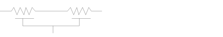
Parallel Reduction
Devices of the same type that are connected in parallel can be combined by “parallel reduction.”
Devices can be connected in parallel regardless of the number of terminals they have. Each terminal of each device must be connected directly to a terminal of the same type on another device of the same type. Terminals must be of the same type if they are defined as permutable. The nets connecting the terminals can have other connections.
The following figure illustrates typical parallel configurations.
If the same device has permuteDevice commands specifying both series and parallel options, both are applied iteratively until no more reduction is possible.
The following figure illustrates complex configurations that reduce to single devices when both series and parallel options are applied.
MOS Reduction
MOS reduction is limited to MOS transistors that can be grouped together if they are of the same type and form a logical function. Such groups form the logic section of NMOS gates and the load and logic sections of CMOS gates.
In normal MOS layout, the gate structures do not have to match the schematic exactly for the circuit to function. All gates have alternative forms. Take for example a three-input AND structure as shown in this figure.
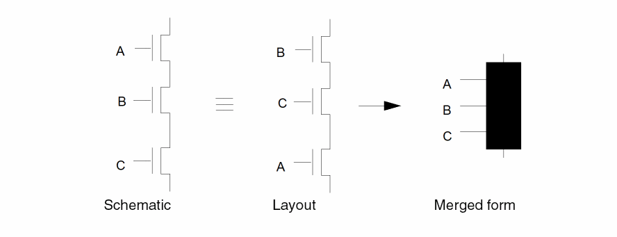
If the schematic has the original transistors in the order A-B-C and the layout has them in the order B-C-A, without MOS grouping the comparison of the circuits fails. The MOS grouping process combines the three separate transistors into a single device with three permutable terminals. With this single device, the terminal ordering doesn’t matter and the layout device matches the schematic device, which causes the original devices to match.
The MOS grouping is done with device pairs in exactly the same way as series and parallel reduction. In this case, however, there are two separate criteria controlling the grouping.
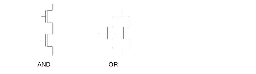
The first grouping criteria is an AND configuration as used in the previous example. If a transistor source/drain connects to the source/drain of another transistor of the same type, and that connecting net has no other connections, then the devices are grouped.
The second grouping criteria is an OR configuration. In this configuration, two transistors have a common net for both their source and drain.
The following figure illustrates AND and OR configurations.
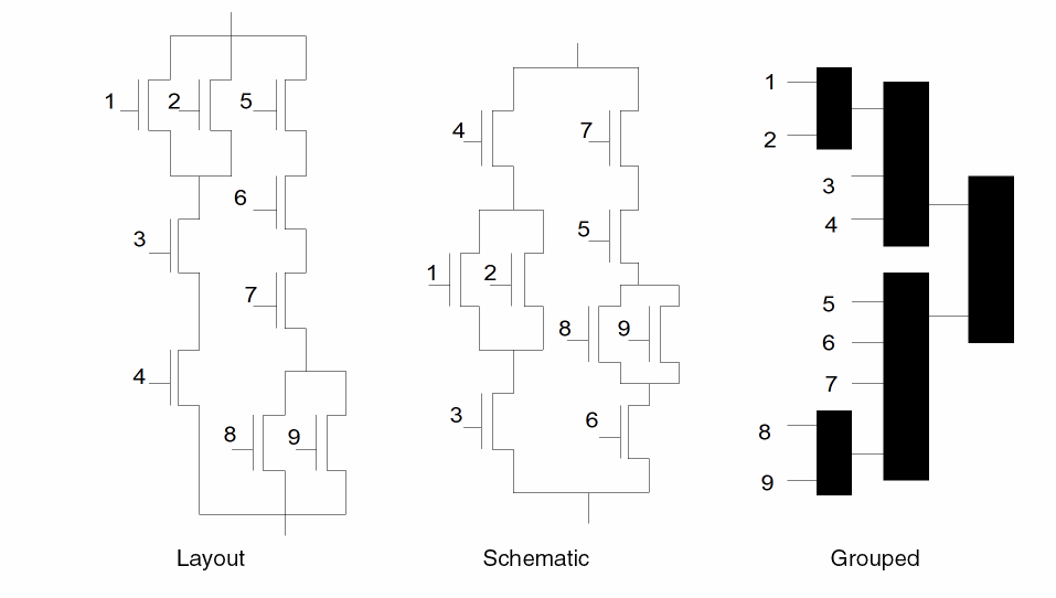
The following figures illustrates how the logic of a complex gate is permutable and how the grouped result is the same for either.
MOS Pseudo-parellel Reduction
During the MOS grouping, Diva LVS can encounter certain transistor configurations that function electrically as if they were in parallel but that do not conform to the conventional concepts of parallel. They are referred to as pseudo-parallel. Diva merges these transistors together as if they were parallel. This merging requires that MOS grouping of the separate AND configurations has been done. Both permuteDevice(MOS) and permuteDevice(parallel) commands must be present in the rule deck for the device being grouped. The following figure illustrates two of these configurations.
Device Pin Permutability
The concept of pin permutability within a device is used throughout the LVS program. For example, source and drain of an MOS transistor are permutable. This means they can be interchanged. This concept extends to larger, more complex devices, where the permutations can be more complex and less obvious.
You define the pins of a device as permutable or fixed by attaching a property to its cell. This property defines whether the pin can be reduced or whether its relationship must stay unchanged. The system netlister adds this information to the netlist so the LVS program can use it.
permuteRule
The recognized keywords in the property are p for permutable and f for fixed. An example of the property contents is
( p 1 2 )
and specifies that terminals 1 and 2 on this device are interchangeable.
(p ( p 1 2 ) ( p 3 4 ) )
which specifies that terminals 1 and 2 are permutable, as are terminals 3 and 4. Also, the pair of 1 and 2 are permutable with the pair of 3 and 4.
The following figure illustrates more complex permutability.
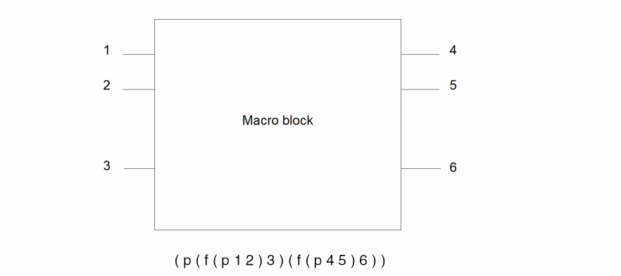
This specifies that terminals 1 and 2 are interchangeable but fixed relative to 3. Terminals 4 and 5 are interchangeable but fixed relative to 6. Group 1, 2, 3 is permutable with group 4, 5, 6.
Ignoring Device Terminals
The ignoreTerminal command forces the program to do its comparison without considering specific device terminals.
During comparison of two networks, it is sometimes useful to be able to ignore specific device terminal types and continue processing as if they did not exist. For example, MOS transistors can be represented with either three or four terminals. The schematic can show the fourth terminal connected to either power or ground. In CMOS this is the substrate or Pwell which, in turn, has contacts to power and ground.
During layout of small areas of the circuit, the Pwell is included, but a connection of power to that Pwell might not be included. A four-terminal verification would show a mismatch with the schematic that has the back-gate of the N-channel transistors connected to power. Larger areas of the layout might include the Pwell contact, but not include a contact to substrate, so the “ground” connection is not made to the back-gates of P-channel transistors. Only in the full layout are all back-gate connections correctly.
It is difficult to modify the schematic each time such a situation occurs. The easiest solution is to reference four terminal devices in the schematic and to tell the LVS program to ignore the back-gates during verification of the smaller circuit areas. On the full circuit verification, the back-gate can be included.
Ignoring Extraneous Devices
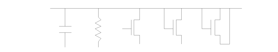
The pruneDevice command tells the program to ignore devices in the circuit that are electrically nonfunctional.
Certain technologies and layout techniques create extraneous devices that are not functional in the final circuit. Examples of this are unused gate-array devices and unused options. These devices are not normally defined in the circuit schematic and appear as unmatched in an LVS run.
For a small number of such devices, the results might be acceptable; but for any significant number, the true matching of the networks is masked. To allow the LVS program to work correctly, you must remove the unmatched devices before performing the comparison.
You can remove (prune) these devices by requesting specific modes of cleanup for specific device types. The program locates all the conditions you specify and removes the devices from further processing.
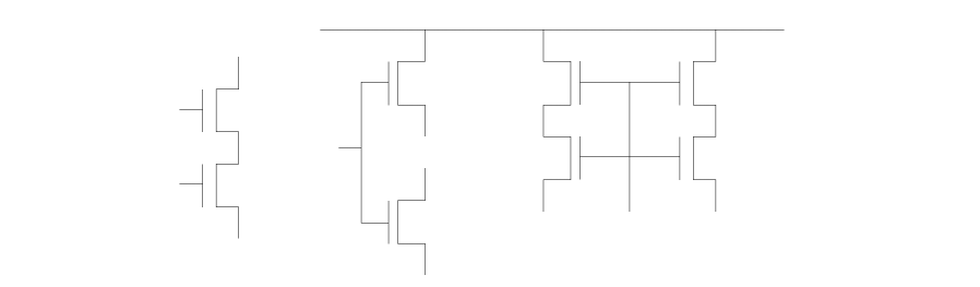
There are two forms of pruning. One eliminates any device if it is connected only to a single net. The other is more complex and is designed for MOS transistors. If the devices have terminal connections that do not contribute to the circuit flow, such as MOS back gates and other bulk connections, you can optionally ignore these during device pruning.
The following figure illustrates various devices that are pruned because they are connected to a single net. The open net ends represent unconnected terminals or nets with no other connection.
The following figure illustrates various transistor configurations that can be pruned. Some devices appear to be connected in such a way that they are not pruned, but the iterative processing removes some devices in the first pass, leaving the remaining devices badly connected. In subsequent passes these devices get pruned.
If you specify parallel reduction, parallel devices are reduced prior to extraneous device removal.
Examples
pruneDevice( MOS "nfet" )
pruneDevice( general "capacitor" )
Removing Unwanted Devices
The removeDevice command lets you remove devices from the network during an LVS run prior to the circuit matching. This command lets you control the removal through a SKILL function that can operate on the device parameters. It also lets you define which terminals of the device to short together and which to leave open.
For capacitors, this device removal exists to some degree by using netlisting control to determine whether a device should be generated in the netlist or not. However, for series devices such as resistors, netlist control cannot merge the remaining nets together. Removing a resistor implies shorting together the original resistor terminals to form a single net from the two original nets. Other devices require a combination of both shorting and opening of nets. For example, a three-terminal resistor has the source and drain shorted but the back-gate left open.
The devices removed by the removeDevice command are treated as if they had been removed by a prune request, and you can see them by highlighting the pruned devices.
Device removal does not affect cross probing. If a removed device is cross probed, there is no matching device. If a net is cross probed, Diva determines whether the net was merged with others due to device removal and highlights all affected nets in both the schematic and layout.
Parameter Analysis
The compareDeviceProperty command lets you request comparison of device properties (parameters) after the devices have been matched.
LVS can compare device parameters defined in the schematic with those extracted from the layout. The schematic parameters are either those specified on the schematic itself for each device instance, or those specified via the netlister as being default values for each device type. The extracted parameters are those derived from the layout by measurement in the extraction program and represent the true values.
The parameters are extracted by the program from the circuit netlist. You can generate them directly in the netlist or via the simulation environment netlisting process, which is driven by the device parameters and the nlpglobals control file. The format of these parameters is defined in the netlist format section of the “Simulation and Environmental Control” appendix.
There are two parts to the parameter processing in the LVS program: the consolidation of parameter values for series and parallel devices, and the comparison of parameters. You can control both parts completely on a device-type basis.
Combining Parameters
To help with a comparison, the permuteDevice command reduces groups of devices of the same type to a single device. For example, to compare three resistors in series on the layout with two resistors in parallel on the schematic, both are reduced to single devices that can be compared by their type and connections. The program does this by reducing devices two at a time iteratively, and alternatively series and parallel, until all series and parallel relationships have been reduced.
Every time LVS reduces a group of devices to a single device, you must combine the parameters for each device to produce a single set of parameters. This enables the parameters to be correctly compared after device matching. The consolidation process is device-, configuration-, technology-, and application-dependent, so you must specify it directly on a device and configuration basis. You cannot combine devices processed by the MOS option of the permuteDevice command.
combineFunction Option
To consolidate, you can use the combineFunction option of the permuteDevice command. This option specifies the name of a SKILL routine that combines the parameters of reduced devices. The routine uses two lists of parameters, one for each device. Each list contains all the parameters for that device. The routine extracts the parameters required for consolidation and combines them. The result, a new list of parameters, is passed back to the LVS program.
The list of parameters you pass back can be the resultant parameters only or a combination of the new ones plus uncombined originals. For example, if the program is consolidating two resistors in series, it uses a SKILL function that has the list of parameters for each resistor. The SKILL function might, in this case, select the R parameter and set Rnew = R1 + R2. It then returns Rnew to the program as the new value of R to be attached to the consolidated device.
The following shows example input:
permuteDevice( parallel resistor resParCombine )
permuteDevice( series resistor resSerCombine )
permuteDevice( parallel nfet nfetParCombine )
Details of the permuteDevice command format can be found in the “permuteDevice” section.
Example
Just as devices are combined two at a time, their parameters can be combined two at a time. The following example illustrates the process.
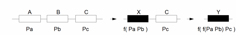
If you have three devices A, B, and C in series, A and B are combined to form X, and then X is combined with C to produce Y. The parameters of A and B (Pa and Pb) are passed to the series device parameter consolidation function, which can do whatever it wants with them, returning a set of parameters that are stored with X. The parameters of X and C (Pc) are then passed to the function which generates the parameters of Y.
This accumulation of parameters works only if the function returns parameters as properties with the same names that were passed to it. For example, if the properties on a device are W and L, the result of the function should generate W and L. To obtain consistent results, the function should also be designed to be independent of the order in which the devices are combined.
Parameter Comparison
After devices on the schematic are matched with devices on the layout, you can compare their parameters. LVS compares the parameters of the actual devices matched. If these are the result of series or parallel consolidation, then LVS compares the combined parameter. However, when you want to display devices with mismatched parameters, Diva highlights the original devices.
To compare the parameters, LVS uses a SKILL routine that you provide. You must give a separate routine for each device type you want to compare.
Use the LVS command compareDeviceProperty to define which devices you want to compare and what comparison routine you want to use. Refer to the “compareDeviceProperty” section for more information on this command. The compareDeviceProperty command works as follows:
- Identifies the devices to be compared.
- Identifies the comparison routine to use.
-
Passes a parameter string from each device to the comparison routine. Each list contains all the parameters for that device.
If a device does not have parameters, LVS passes a null string. In the case of the schematic, LVS passes the default string associated with the device type (see netlist format in Appendix D, “Simulation and Environment Control,”) if it exists; otherwise, LVS passes a null string. -
The routine compares the lists and returns a true or false value, where t (true) indicates that the comparison has failed. You can replace the true switch with a message string that can be used by Explain Error in the LVS form.
When the routine returns a message string, you must limit the length of the string to less than 32,000 characters. -
If the comparison fails, LVS stores the devices in error in the audit.out error file. Display Errors in the LVS form uses this file to highlight errors on the schematic and layout.
If LVS is comparing combined devices, it compares the combined parameters, and updates the error file with references to all the original devices forming the consolidation.
You can view the devices in error graphically by selecting the Display Errors UnMatched parameters option in the LVS Error Display form. This option highlights those devices. You can determine the corresponding device in the alternate cellview (schematic or extracted) by using the cross-probing capability.
Parameters for Ambiguity Resolution
Normally, LVS matches circuitry using only the device types and their interconnections. When an ambiguous area of circuitry is encountered, the program has a choice in what can be matched. This approach might be acceptable for the connectivity, but it can result in mismatched device parameters where the ambiguous branches of the circuit actually contain different device parameters.
The ideal situation is for LVS to take into account the device parameters in its matching algorithm when ambiguous circuits are encountered. However, the parameters should not be used when matching straight connectivity.
Since the program has no way of knowing which device parameters to use to aid the verification, users must provide feedback to the program in terms of the parameters to be considered and their effect. For example, users must specify whether parameters should be within a certain percentage of each other or whether they should be identical to form a match.
To resolve this issue, LVS lets you define a command that instructs it to use parameters as part of the LVS signature process. The form of the command is
parameterMatchType( "device" function )
Explanation
The device is the name of the device type whose parameters are to be used. The function is the name of a SKILL function that provides feedback to Diva on parameter information.
The main matching capability in LVS is based on signature analysis. For ambiguous areas of a circuit, the program needs to add the device parameters into its signature. However, the program does not know which devices to process and which parameters from all the possible parameters on a device to use. Also, the program cannot reasonably handle floating point parameter values, which is a critical situation. If one device parameter is 1.0 and another is 1.00000001, and the program takes these numbers literally, it would consider them to be mismatched. This can also be extended if you consider “close enough” to be correct. For example, if one parameter is 100 and the other parameter is 99, this might be considered a match.
The above command tells the program which devices it should look at and gives you control of the parameter selection and value interpretation.
The program passes the parameter list from the device to your function. Your function must return a single integer value. This integer value can be derived any way that you want and normally represents the value of the key parameter or parameters being considered as critical to the matching. The returned value can be considered as a classification of the device into a subtype. Only devices of the same type and subtype are matched.
Warning
The program goes through two stages as follows:
- It tries to match without considering parameters.
- If it finds ambiguity and parameter matching is requested, the program adds the value returned from your function into each device signature. The program then tries to match again.
If the second matching is unsuccessful, the program does not return to the original mode for the ambiguous devices. The program does not assume that all ambiguous devices are equivalent and does not make a random matching. If this occurs, the ambiguous part of the circuit remains unmatched.
Be careful with the value returned from the function. If you are only considering device lengths of 2, 3 or 4, you can just use the length as the returned value. However, if you are considering parasitic capacitance values as the matching criteria, you must be sure that the function returns the same integer value for all capacitance values that you want matched. If you want a tolerance on the matching of parasitic values, you should consider rounding, truncating, or even multiplying the parasitic value by a factor before these operations.
The returned value should be considered a device subtype and not a value. Devices with the same subtype are matched. The user’s function creates a subtype from the device parameter list.
Limitations
Using the parameters to aid matching only works where the parameters are known. This is true for individual basic devices and for results of series and parallel reduction where the user's parameter reduction function has been called.
It is not true for permutable MOS devices in AND and OR configurations. The program reduces these groups of devices to higher-level structures and matches these. At this stage, the individual parameters of the component devices are not available for controlling the matching.
SKILL Routines Format
You must place the SKILL routines that perform parameter reduction and comparison in the lvsRules function, before the various LVS control commands (permuteDevice, ignoreTerminal, pruneDevice).
In the following examples, the comments clarify the application of the LVS program but do not describe the basic SKILL structure or syntax. For information on SKILL refer to the Virtuoso Design Environment User Guide
Both the permuteDevice and compareDeviceProperty SKILL routines process two parameter lists. The first parameter list in compareDeviceProperty is always from the layout representation, and the second list is from the schematic. The order is important in comparisons where some check other than equality is required.
The contents of the routines can be as complex as you want, and can use any of the parameters in the property strings associated with the devices. For example, you can calculate the width and length resulting from combining two transistors using their original widths and lengths plus parameters such as bend counts, plus any constants or factors you want.
You can also use the permuteDevice function to determine whether series or parallel reduction should take place for the two devices being processed. This is achieved by the function returning a flag that tells the program not to perform the reduction.
Example 1
The following is an example of an SKILL function that performs a parameter combination in the permuteDevice command. The numbers at the beginning of the line are for reference in the comments only and do not appear in the final code.
1    procedure( parallelMOS( m1, m2 )
2     prog( ( mt )
3      mt = ncons( nil )
4      if( ( m1->L && m2->L )
5       mt->L = ( m1->L + m2->L ) / 2.0
6      )
7      if( ( m1->W && m2->W )
8       mt->W = m1->W + m2->W
9      )
10      return( mt )
11     )
12    )
Defines the procedure name parallelMOS which is the name used for the function in the permuteDevice statement. It also defines two arguments, m1 and m2, which it expects to receive when the LVS program calls the function. These two arguments are each lists of parameter properties and contain all the properties available on the devices being combined.
Set up a local variable as a list (initially a null), which contains your resulting parameter list for the combined device.
Checks to see if both the m1 and m2 lists contain a reference to a parameter called “L.” If they do, line 5 calculates a resulting value as (L1+L2)/2 and stores it in the new list “mt” with the parameter name of “L.”
Checks to see if both the m1 and m2 lists contain a reference to a parameter called W. If they do, line 8 calculates a resulting value as W1+W2 and stores it in the new list mt with the parameter name of W.
Returns the resulting list “mt” back to the LVS program, where it is associated with the combined device.
Example 2
The following is an example of a compareDevice SKILL routine which compares two parameters and returns an error status if the parameters do not conform to the required limits.
1    procedure( compareCap( m1, m2 )
2     prog( ( )
3      if( ( m1->C && m2->C )
4        if( abs( m1->C - m2->C ) > 0.01 * m2->C
5         return( t )
6        )
7      )
8       return( nil )
9      )
10    )
Defines the procedure name compareCap which is the name used for the function in the compareDeviceProperty statement. It also defines two arguments, m1 and m2, which it expects to receive when the LVS program calls the function. These two arguments are each lists of parameter properties and contain all the properties available on the devices being compared. The first (m1) contains the properties for the layout (extracted) device, and the second (m2) contains the properties for the schematic device.
Checks to ensure that both lists contain the parameter to be compared, in this case C.
Compares the parameters and, in this case, tests to see if the extracted C is within 1% of the schematic C. If it is not, the function returns t (true) which indicates to the LVS program that an error must be generated. If it is, within 1% the function returns nil (false) which indicates that no error has occurred, in which case the LVS program takes no further action.
Returns the result, in this case, the value nil. To indicate an error, it might return the value t or a text string. This text string is associated with the error in the database and displayed when you select Explain Error on the Error Display form, which you access from the LVS form.
Two ways of creating a text string are as follows:
return ( "Parameter mismatch on MOS devices" )
This text string is fixed for the compare routine and does not contain parameter values.
sprintf( x , "Param mismatch: %g to %g",
float( m1->C ), float( m2->C ) )
return( x )
This text string contains the values of the parameters compared.
Device Fixing
The Apply Device Fixing option in the LVS form lets you control the permutability of devices on an instance-by-instance basis. Permutability normally applies to all individual devices of the type you specify. There are times, however, when you might not want global permutability. You can have the majority of your circuit obey the global permutability requests but force selected individual devices to be compared without permutability.
Some specific gates within a circuit are valid only if they are formed on the layout with exactly the individual transistor relationships defined in the schematic. Alternatively, some gates might function correctly only if specific devices in them maintain positions relative to others. For example, the clocking device in an NMOS NAND gate might need to be directly connected to ground while the other devices might be interchangeable.
You can fix series, parallel, and MOS permutability, and you can specify two types of fixing, fixing device and order fixing device.
-
fixing device
A fixed device does not take part in device permutability processing and must, therefore, have direct correspondence between the layout and schematic. -
order fixed device
An order fixed device does not allow the fixeddevice terminals to be switched, but it can take part in device permutability processing.
Prerequisites
Device fixing has the following requirements:
- You must define the devices to be fixed in the schematics cellview.
-
You must set a global switch to turn device fixing on.
Only one of the circuit representations (schematic or layout) has to be fixed since the other must conform to it; fixing both might lead to unresolved conflicts. We choose the schematic as the representation to be fixed since LVS considers it the master to which the layout must conform. - You must manually add control information to the netlist if you run LVS on a netlist generated in some way other than through the netlister. The netlisting program translates any fixing information provided on the schematic into specific control lines in the netlist. If the netlist is not generated by the system netlister, it does not have these lines.
The fix Property
You can fix devices in the schematic by adding a property to device instances. The property has the following form:
fix = " terminalName [order] terminalName [order] ... .... "
fix is the name of the property. It must be of type nlpExpr.
terminalName contains the names of one or more terminals of the device instance to which you want to attach the property.
order determines the type of fixing. If this keyword is specified, “order fixing device” will be performed. Otherwise, “fixing device” will be performed.
The device instance to which you attached the property can be a single low-level device such as a transistor, a higher level device such as a gate, or a high-level structure such as a counter. You cannot attach the property to the complete circuit.
All of the lowest level devices within the instance that are connected to the named terminal are considered fixed. For example, if in a CMOS NAND gate, you reference the terminal “in1” in a fix property, both the n and p devices gated by in1 are fixed.
For a higher level device, such as a counter stage containing gates, which in turn contain transistors, the fixing applies to all transistors connecting to the named terminals, throughout the hierarchy. If the fixed instance is contained within another level of hierarchy, all placements of that higher level instance contain fixed lower level instances.
Correspondence Points
The Correspondence Points field lets you define correspondence points to aid the LVS processing. You can use terminals as correspondence points and/or provide a correspondence point file.
A correspondence point is a predefined matching of a single location in the layout and schematic that you supply and that is available to the program to help in its comparison. Normally in the LVS program correspondence points are not required; but in some cases of unresolved ambiguity, they help the program make a decision.
If you supply a correspondence point between two items that do not actually match, the program might immediately recognize the discrepancy and ignore the point; or it might initially accept the point and propagate errors to the surrounding circuit. The latter occurs if the incorrectly labeled nets have the same number of connections.
You can define correspondence points in two ways. Both can be applied at the same time.
-
By using terminal names
The program can use any terminal (pin) names on the schematic and extracted layout as correspondence points. It automatically transfers the names from the schematic or extracted representation to the netlist as t statements.
If you choose the terminals option in the LVS form, these statements are used as correspondence points. If a terminal name on the layout corresponds to a terminal name on the schematic, then LVS assumes they refer to the same net. This feature does not apply to net names. -
By creating a correspondence point file
You can specify your own correspondence points by creating correspondence point files using the LVS Correspondence Points form.
Because the application of incorrect correspondence points can mislead the program, first try running the program with none defined. If ambiguity causes the comparison to fail, you can apply circuit terminal names. If the run without terminal correspondence compares correctly, check your labeling by probing your terminals to confirm that the names used correspond to the names of the nets that the LVS program has matched.
Creating a Correspondence Points File Using a Form
You can create correspondence points using the Correspondence Points form, which you access by selecting Create in the LVS form. You select pairs of items, one each from the extracted and schematic cellviews, to be stored in a correspondence points file. It is a standard text file containing net and device names. You can create any number of files with different names and then specify which one you want in the LVS form.
When using the Correspondence Points form, you must use the extracted and schematic cellviews you defined in the LVS form. Each cellview must be open in a window. You can be at any level of hierarchy within the cell.
Correspondence point files are a normal part of your computer file system and are not changed or deleted by running LVS. A temporary lvs.cpoint file is left in your run directory after the run. This contains the correspondence point file data, with net and device numbers instead of names.
The name lvs.cpoint is a reserved name and should not be designated as a user-defined correspondence file name.
Creating a Correspondence Points File Manually
You can also create correspondence point files by manually editing a file. You must know the names of the devices and nets you want matched. To edit the correspondence file manually, you need to understand that:
- Each line of the file describes a single correspondence point
-
Each line has one of the following formats:
( #net_path_name ) ( #net_path_name )
( $device_path_name ) ( $device_path_name )
The left-hand name refers to the layout, and the right-hand name refers to the schematic.
The “#” and “$” define nets and devices, respectively. There must be no space between the character and the name.
There must be one or more spaces between the opening and closing parenthesis and the names, and one or more spaces between the layout and schematic definitions. The number of spaces before the layout definition is not significant.
Network Terminal Processing
LVS uses network terminals (as distinct from device terminals) in Network Terminal Processing in several ways.
-
Terminals are created by placing pins - not labels - in your layout view. During the extraction process, Diva attaches the pin name information to the net in the resulting extracted view. This pin name information from the extracted view is used as terminals during an LVS comparison.
- Terminal names automatically give additional information. The program generates error messages for terminals that do not match. See the “Unmatched Terminals” section for more information.
- If a terminal name exists in both cellviews, devices cannot be permutated across that terminal. No series, parallel, or MOS permutation absorbs a terminal.
- If you select the terminals option in the LVS form, LVS treats all terminals with the same name in both cellviews as correspondence points. This forced matching of the terminals does not force the nets to which they are attached to be matched if they do not actually match. However, forced matching does help to resolve ambiguities.
Comparing Macro Cell
The LVS program works on all device types, regardless of whether they are low-level transistors or high-level macro blocks. The comparison works from two netlists, each derived from a different representation of the circuit. In the normal case, one is from the extracted layout and one from the extracted schematic. It is the control of the netlister that is special for macro cells.
The netlister normally defaults to the spice or schematic representation when encountering a device to translate. For macro cells, the default has to be overridden by use of the simulator control commands for the switching lists and stopping lists in the file .simrc in your home directory. (Refer to
In addition, the cellview being referenced must contain the NLPModelPreamble and NLPElementPostamble properties that control the netlister output. If you put these on the layout cellview, you can automatically propagate them to the abstract cellview by using the abgen program.
When processing the schematic, the netlister follows its normal procedure and assumes global signals of the same name are connected. For the extracted cellview, however, this function is disabled so that true breaks in the global signals are not hidden.
With these changes in place, the processing of LVS remains unchanged. All its normal features and facilities are available.
Output Files
Diva puts all the errors it finds in error output files which it uses to display and explain errors.
The output files are stored in subdirectories of the run directory. When you use the LVS form, you must specify the run directory where you want to put your results. The program then creates the run directory (if one does not already exist) and the layout and schematic subdirectories. When you run an LVS comparison, the resulting error output files are put in the appropriate subdirectories.
The outputs from LVS fit into the following categories:
- Error files that you can read to find the name of the net, device, or terminal causing an error.
- Working and information files that you can display by using menu commands.
- Control and cross-reference files that you cannot access.
- A copy of the rules file under the name divaLVS.rul
Error Files
A series of text files containing the error output of the LVS program is stored in the layout and schematic subdirectories of the run directory.
Diva highlights the nets and devices referenced in these error files when you select the appropriate entry in the LVS Error Display form. However, with a complex design you might want to display only one net or device at a time. You can do this by using the Probe command and entering the net or device name.
One way of finding the net or device names is to look them up in the error files. Each file entry consists of two lines. The first gives the name of the object in error and indicates if it is a net (N), device (I), or terminal (T). The second line is a comment line explaining the error.
N <netName> [comment]
<explanation>
I <deviceName> [comment]
<explanation>
T <terminalName> [comment]
<explanation>
The error file names and their contents are as follows:
netbad.out        Lists all unmatched nets
devbad.out        Lists all unmatched devices
prunenet.out        Lists all ignored nets
prunedev.out        Lists all ignored devices
mergenet.out        Lists all merged nets
termbad.out        Lists all unmatched terminals
audit.out        Lists all unmatched parameters
Working and Information Files
The following files contain information that you can display using the Show Run Info form, which you access from the LVS form.
Text file containing the netlist of the schematic circuit. You can view this file by selecting the Schematic Netlist option in the Show Run Info form.
Text file containing the netlist of the extracted circuit. You view this file by selecting the Layout Netlist option in the Show Run Info form.
Text file containing all messages and warnings output from the program. You can view this file by selecting the Output option in the Show Run Info form.
Text file containing information on the program execution and its environment. It also includes summary information of the results of the functions you requested. You can view it by selecting the Log option in the Show Run Info form.
LVS Ambiguity File
The ambiguity file shows the choices that Diva LVS makes when unable to proceed with normal matching due to ambiguity in the netlists. Each entry indicates the type of match: device or net, followed by the list of layout and schematic device or net numbers which could be matched. The pair, or pairs, that are chosen are indicated with arrows.
When all else fails during debugging, you can examine the choices that Diva LVS made to resolve ambiguity and over-ride those choices by adding correspondence points.
Note:- When you add correspondence points the sequence of matches made will change and the content and order of the information in the ambiguity file may change.
- The format of the ambiguity file is not fixed and is subject to change without notice. The ambiguity file may be removed or replaced in a future release.
Displaying Errors
When LVS has completed running, you can display the errors or cross reference the matching nets and devices. All error display is in the form of probes (highlighting).
You can display errors by selecting Error Display in the LVS form. You also can manipulate displayed errors using the Probe command from the Verify menu. By using the LVS output error files, you can identify specific nets or devices that you want to probe. You can find a description of the output error files in the Output Files section. You can probe nets and devices using the Probe command from the Verify menu.
The following sections discuss the display options available in the LVS Error Display form.
Unmatched Nets
The nets option under the Unmatched heading highlights all nets that failed to match in LVS. The number of connections made to the net is displayed when you use select Display Errors. Unmatched nets do not include merged nets.
Merged Nets
A second class of unmatched nets is the merged nets. In some cases, LVS recognizes that two nets need to be “shorted” together to improve the comparison. This occurs when many of the instances attached to the nets have already been matched. Explain Error in the LVS Error Display form lists the names of the two merged nets. LVS highlights not only the error net, but also the net with which it was merged.
When two nets need to be merged in the extracted representation, it indicates the possibility of an open. When two nets are merged in the schematic representation, it indicates the possibility of a short in the layout.
Unmatched Instances
For the selected window, LVS highlights all instances (devices) that appear in that network and could not be matched with instances in the alternate network. For schematic device instances where the device displayed is not the lowest level in the hierarchy (for example, a transistor is in error, but the display shows the logic gate that contains it), the complete higher level device is highlighted. You can use the Push View command in the Hierarchy menu to display the individual devices. The mismatched devices are highlighted and those that match are not.
Unmatched Parameters
For the selected window, LVS highlights all instances (devices) that appear in that network and whose parameters violated the requested comparison with instances in the alternate network.
LVS compares parameters only when the instances match in the two representations. Therefore, you can find the corresponding instance for any parameter mismatch in the alternate representation by using the Probe command.
Any instances that did not match and appear in the unmatched instances display have not had their parameters compared.
For devices that have been combined in series or parallel and whose parameters have been combined by the function supplied to the permuteDevice command, the parameter comparison is made on the resulting values. When there is a mismatch, LVS highlights all the devices involved.
Unmatched Terminals
The Unmatched terminals option in the LVS Error Display form under the LVS form highlights terminals that failed to match. There are two kinds of mismatched terminals in this display.
The first are terminals at the top level of the design hierarchy. These terminals correspond to pins used to make connections to the rest of the design. Terminal checking is done after all matching has completed. Those terminals that are in both designs are checked to make sure they match each other. This is very important in Place and Route applications where connections are made to the pins. If a nonglobal terminal exists in one netlist, but not in the other netlist, an error is flagged unless the terminal is not connected to any devices. If a global terminal’s name in one netlist does not match to another global terminal’s name in the other netlist, an error is flagged.
The second kind of terminal mismatch is internal to the design. Under certain special circumstances, LVS recognizes that a better match can be made by switching the terminal connection of an instance from one net to another. This is referred to as a rewired terminal. For this to occur, many of the instances and nets in the local region must have already matched. This kind of error occurs when two nets are cross-wired. The LVS program interchanges the connection and continues processing.
LVS does terminal rewiring only in the extracted database. The schematic database is taken as the master.
The error message produced by a rewired terminal is very explicit. For example, it might say, “Terminal ‘gate’ of /m25 should be connected to /clock2 instead of /clock1.” In this case, LVS connects /clock2 to the gate and continues running. This makes cross probing nets somewhat confusing. If you try to cross probe the gate of /m25, it selects net /clock1 and cross probes it. However, because LVS rewired the gate internally, it believes /clock2 is the gate net. Therefore, to cross probe the gate, first probe /clock2 by name to highlight it and then cross probe it.
Rewired terminals often occur in pairs. By inspecting the pairs, you can see which nets have been cross wired.
There is usually more than one way to repair a cross-wired situation. For example, even in the simple example of a crossed pair, you can correct the error at either end of the nets. LVS might not find the terminal switching that is most appropriate for the your design. You must decide on the best way to correct the design.
Pruned Nets
This is a display of all the nets that were removed from the LVS processing with the command pruneDevice.
Pruned Instances
This is a display of all devices that were removed from LVS processing with the pruneDevice command. This file also contains the devices removed by the removeDevice command. The removed devices are differentiated from the pruned devices by the associated message that displays when you query the device highlight.
LVS Verification Rules Commands
compareDeviceProperty
compareDeviceProperty( device compareFunction )
Description
Defines the name of the SKILL function used to compare properties of devices matched in the layout and the schematic. It applies to the device type specified.
Fields
Name of the device type to be compared. It consists of a character string enclosed in quotes.
SKILL function name. This function compares the parameters of pairs of devices that are matched in the layout and schematic. Parameter values are stored on devices as properties.
The function can return the following values:
- The value nil indicates the parameters match.
- The value t indicates the parameters do not match.
- A text string indicates the parameters do not match. The string is used as a label for the mismatched flag.
Examples
The following example calls a SKILL function that compares parameters of all nfet devices.
compareDeviceProperty( "nfet" nfetCompare )
The following example calls a SKILL function that compares parameters of all capacitor devices.
compareDeviceProperty( "capacitor" capacCompare )
ignoreTerminal
ignoreTerminal( device terminal )
Description
Specifies which terminal types on which device types to ignore during the comparison.
Some comparisons might need to totally ignore a device terminal. A good example of this is a back-gate in CMOS that is correctly connected in the schematic. In the layout, however, whether it is connected or not can depend upon the size of the cell being processed. A small cell might not contain the layer to which the back-gate should be connected. A larger layout might have the layer but not have it connected to the correct net. Only on the final composite is everything in place to correctly connect the back-gate. A layout to schematic comparison always fails in the first two cases unless the back-gate is ignored.
You must specify a separate ignoreTerminal command for each terminal you want to ignore.
Fields
Name of the device type whose terminal is to be ignored. It consists of a character string enclosed in quotes.
Name of the terminal type to be ignored. It consists of a character string enclosed in quotes.
Examples
The following example ignores all bulk terminals of nfet devices during comparison.
ignoreTerminal( "nfet" "B" )
The following example ignores all bulk terminals of pfet devices during comparison.
ignoreTerminal( "pfet" "B" )
lvsOption
lvsOption (keyword value)
Description
lvsOption lets you control specific options that affect basic LVS algorithms.
Prerequisites
This function must only be used within lvsRules().
Arguments
Controls the reduction of pseudoparallel devices During MOS reduction.TRUE Runs pseudoparallel reduction in this LVS run.FALSE Does not run pseudoparallel reduction in this LVS run.
The default value for REDUCE_PSEUDO_PARALLEL is TRUE. Only one value for REDUCE_PSEUDO_PARALLEL may be specified for the entire run. For example you cannot turn pseudoparallel reduction on, execute several LVS commands, and then turn pseudoparallel reduction off. The value for REDUCE_PSEUDO_PARALLEL in the final lvsOption command will be applied to the entire lvsRules() run.
See the MOS Pseudo-parellel Reduction section earlier in this chapter for a discussion of pseudo-parallel configurations and how Diva LVS treats them.
Controls checking for terminals that match but have different direction modifiers.TRUE Enables the check for different terminal direction modifiers. This is the default value.FALSE Disables the check for different terminal direction modifiers.
Controls the reporting of devices that are mentioned in the rules but do not exist in the netlist.
NONE Prevents the reporting of unknown devices.
BRIEF Reports unknown devices in a minimum number of lines by listing several devices per line of output. This is the default setting.FULL Reports unknown devices as one line per device.
Controls the order fixing for device in MOS reduction.
TRUE Specifies all devices in the fixing property as order fixing devices.FALSE Uses the fixing property already specified.
Controls the checking and reporting of unmatched terminals.NONE Does not report any unmatched terminals in layout or schematic. This is the default.LAYOUT Reports unmatched terminals in layout (first netlist).SCHEMATIC Reports unmatched terminals in schematic (second netlist).BOTH Reports unmatched terminals of both layout and schematic.
Example
lvsRules(
....
lvsOption(REDUCE_PSEUDO_PARALLEL FALSE)
permuteDevice(MOS nmos)
permuteDevice(parallel nmos someFunc)
lvsOption(ORDER_FIXING TRUE)
lvsOption(EXTRA_TERMINAL_REPORT BOTH)
...
)
parameterMatchDegree
parameterMatchDegree ( device procedure )
Description
Defines the name of the SKILL procedure used to compute the degree of parameter mismatch between a device in the layout and a device in the schematic. It applies to the device type specified.
This command is intended to be used to help resolve ambiguity during the matching process. After the matching process has found all the matches it can find based only on the circuit topology, groups of devices which are topologically the same are considered. Every possible pairing of schematic and layout devices in each group are passed to the SKILL procedure for evaluation of how well the device properties match. The pair with the least amount of mismatch is then matched.
Fields
The name of the device type for which the function applies. It consists of a character string enclosed in quotes.
The name of a SKILL procedure. This procedure computes the degree of parameter mismatch for pairs of devices in the layout and schematic. Parameter values are stored on devices as disembodied property lists.
The procedure can return the following values:
The value nil indicates an infinite parameter mismatch; the pair of devices in the layout and schematic are never matched.
A positive float or integer value which is the degree of parameter mismatch for the pair of devices. The smaller the value, the better the match for the pair of devices being considered.
Examples
The following example calls a SKILL function to compute parameter matching degrees of all res resistances.
parameterMatchDegree( "res" resDegreeComp )
The following is an example of a rule file that includes a parameterMatchDegree rule. It calculates a percentage difference between the resistance values of the layout and schematic devices.
lvsRules(
; ** Match degree Procedures **
procedure( resDegreeComp( layRes schRes )
prog(( nearZero degree value1 value2 )
   nearZero = 0.0000000000001
   if( layRes->R then
    value1 =  layRes->R
   else
    return( nil ) ; ** if no value, return nil. **
   )
   if( schRes->R then
    value2 =  schRes->R
   else
    return( nil ) ; ** if no value, return nil. **
   )
   if( abs( value2 ) < nearZero then  ; ** value2 is close to 0 **
    degree = abs(value1 - value2)
   else
    degree = abs((value1 - value2)/value2)
   )
   ;; return value
   return( degree  )
  ) ; ** prog **
 ) ; ** procedure resDegreeComp **
parameterMatchDegree( "res" resDegreeComp )
)
parameterMatchType
parameterMatchType ( device Function )
Description
Defines the name of a SKILL function to be used to process parameters for a device when the program encounters ambiguous circuits. The program uses the result of the function to resolve matching of the ambiguous circuits.
Fields
The name of the device for which parameter matching is to be used during ambiguous circuit matching.
The name of a SKILL function. The SKILL function is passed two arguments: the name of a device and a disembodied property list containing the parameters on the device. The function must return a fixed point integer. The integer is used to match devices with the same parameters. To return an integer, use the fix() function to return an integer so that there is no ambiguity from floating-point round-off.
If you are trying to match on MOS Width, for instance, multiply width by 1,000 before converting to integer in order to use three decimal places of accuracy. For instance, if you had 0.0012 and 0.0017, multiply by each by 1,000 to give you 1.2 and 1.7. When you convert to integer, both numbers become one.
Do not multiply by a very large number since that effectively asks for infinite accuracy and will have exactly the same problem as a floating-point number does.
Examples
The following example shows the definition of the SKILL function followed by the use of that function in the parameterMatchType command.
 procedure( fetWidthDiff( deviceName dpl )
  if( dpl->w then
  fix( 1000 * dpl->w )
  else
  0
)
)
....
parameterMatchType( "nfet" fetWidthDiff )
parameterMatchType( "pfet" fetWidthDiff )
permuteDevice
permuteDevice( type "device" [term1] [term2] [combineFunction] )
permuteDevice( MOS "device" )
Description
This command specifies which form of circuit simplification to perform for a specific device type. The simplification is based on the permutability characteristic of the device as derived from the device definition in the netlist.
You can specify multiple options for a single device by defining multiple permuteDevice commands. When you specify multiple options, the system applies all options iteratively as reduction takes place.
Arguments
You need different permuteDevice commands for each of the options: to apply parameter consolidation, provide a separate combine function name for each command having series or parallel options. These combine function references can be for the same or for different functions.
This parameter-combining function does not apply for MOS grouping.
The function returns the values described below. If you do not provide a function or the devices do not have parameters, parameter consolidation cannot take place although the devices are still combined.
- A disembodied property list containing the resultant parameters that is added to the resultant combined device.
-
A text string of the value
doNotCombine, which tells the program to not combine the two devices in series or parallel. -
A symbol of the value
doNotCombine, which tells the program to not combine the two devices in series or parallel.
Examples
The following example reduces resistor devices in parallel before comparison.
permuteDevice( parallel "resistor" )
The following example reduces capacitor devices in series before comparison.
permuteDevice( series "capacitor" )
The following example reduces capacitor devices in parallel and calls a SKILL function to combine the device’s parameters before comparison.
permuteDevice( parallel "capacitor" parCapMerge )
The following example reduces resistor devices in series and calls a SKILL function to combine the device’s parameters before comparison.
permuteDevice( series "resistor" serResMerge )
The following example reduces nfet devices in AND or OR configurations and swaps input terminals during comparison.
permuteDevice( MOS "nfet" )
The following example illustrates the series reduction of a multiterminal device.
permuteDevice( seriesN "res4" "anode" "cathode" res4merge )
pruneDevice
pruneDevice( type device [terminal] )
Description
Ignores inactive devices in the circuit. It functions as if the devices were totally removed or pruned from the circuit.
In some designs or design methodologies, such as gate array, the layout contains unused devices that have no equivalent in the schematic. These unused devices can cause a mismatch between the layout and schematic, and possibly mask or confuse real errors. If these devices are electrically inactive, they can be safely ignored.
The pruning process is iterative and takes place during reduction. The removal of one inactive device can make another device inactive, which in turn is pruned.
Fields
Defines the type of pruning to be performed. The options are as follows:
Prunes devices connected to a single net.
Prunes MOS devices whose connectivity guarantees they cannot affect the function of the circuit. The conditions for this are that either their source or drain is not connected to any other device in the circuit, and the gate is not driven. A gate that is not driven can connect to other MOS gates but nowhere else.
Also prunes MOS devices with the source, drain, and gate all connected to the same net.
When considering the connectivity for pruning, this command treats terminals of the circuit as if they are connections to another device. This ensures that any device connected to a terminal is considered driven. The program recognizes terminals automatically from the pins in the layout.
Name of the device type to which the pruning is to apply. The name consists of a character string enclosed in quotes or a number of separate strings, each enclosed in quotes with the list of strings enclosed in parentheses.
Name of the terminal type to be ignored during device pruning. The name consists of a character string enclosed in quotes or a number of separate strings, each enclosed in quotes with the list of strings enclosed in parentheses.
The terminal name applies to all device types specified. If no device types have terminals with this name, the program continues and a warning message is issued.
If this terminal name is specified, the devices are pruned as if the terminal does not exist. The terminal is retained for all other processing.
Examples
In this example, during comparison all nfet devices that are configured in compliance with MOS mode are ignored.
pruneDevice( MOS "nfet" )
In this example, during comparison all capacitor devices that are configured in compliance with general mode are ignored.
pruneDevice( general "capacitor" )
In this example, during comparison all nfet and pfet devices that are configured in compliance with general mode are ignored.
pruneDevice( general ( "nfet" "pfet" ) )
In this example, terminal B for the three terminal resisters is ignored. For pruning, it is regarded as a two-terminal transistor.
pruneDevice ( general "res3" "B" )
removeDevice
removeDevice ( type [short(term-list) ...] [function])
Description
Removes specific devices from the circuit based on the device type and the function you can optionally specify, which operates on the device parameters.
With this command, you can specify whether the terminal nets are left open or shorted together.
Fields
Name of the device type, in double quotation marks, to be removed. Instances of this device are removed in both the layout and schematic (depending on the use of the function option).
An optional keyword that introduces a list of terminal names. All terminals in this list are shorted together when the device is removed. You can specify more than one short keyword and associated list. Terminals in each short list are shorted to other terminals in the same short list, but are not shorted to terminals in other short-lists.
All remaining terminals of the device not in the short lists are left open when the device is removed. If you do not specify the short option, all terminals are left open when the device is removed.
An optional argument that defines the name of a SKILL function previously defined in the rules file.
If you specify the function argument, Diva calls the function prior to removing the device. If the function returns t, the device is removed. If the function returns nil, the device is not removed.
If you do not specify the function argument, all devices of specified type are removed.
Diva passes the list of parameters on the device to the function. The intent of the function is to analyze the list of parameters and decide whether or not the device should be removed.
Examples
The following example is the simplest form of the command. The capacitors are removed and the connections are left open.
removeDevice( "cap" )
The following example removes the resistors and shorts their terminals together:
removeDevice( "resistor" short( "PLUS" "MINUS" ))
The following example includes two separate terminal shorts and a function which operates on the device parameters. It removes the device only if the size parameter is equal to 1.
procedure( myFunct( plist )
    prog( ( )
      if( (plist && plist->size == 1 )
     return( t )
   )
   return( nil )
 )
)
removeDevice( "xyz" short( "a" "b" ) short( "c" "d" ) myFunct )
Backannotation (lvsbx)
Description
This function performs backannotation of schematic instance and net names to the extracted view of the circuit generated by the Diva verification extraction.
Prerequisites
Before you specify this function, you must create an extracted version of the layout and run LVS between the extracted and schematic views.
Operation
Backannotation is performed by a stand-alone program. It reads instance and net names from the schematic and uses the files created by the LVS run to create a copy of the extracted view updated with the schematic names.
You can either create an annotated copy of the extracted view, or you can overwrite the original extracted view.
There is no difference in disk or virtual memory usage between creating a new extracted cellview and overwriting the original extracted cellview. Both operations create a new version of the cell in the library.
Execution
Use the following command in the UNIX environment to execute backannotation:
lvsbx < run_dir > [ library cell view ]
You must run the lvsbx program in the directory you ran the graphics editor when you executed LVS.
You must specify the run_dir argument that defines the name of the run directory previously used for an LVS run. Diva determines the schematic and extracted cellviews to be processed from the si.env file in the run_dir directory.
The library, cell, and view form a single optional argument that defines the name of the output cellview. You must specify all three of these options or the argument is not valid. If you specify this argument, the backannotated extracted cellview is written to the view specified. If you do not specify this argument, the original extracted cellview is overwritten.
Limitations
Only flat extraction is supported. Diva does not backannotate to a layout that has been extracted hierarchically.
Names of instances and nets that are hierarchical in the top level of the schematic are modified to create flat names in the extracted view. For example, Diva converts the schematic hierarchical name of /I1/net2 to the flat name |I1|net2 in the extracted view.
If you overwrite the original extracted cellview, the cross-probe capability from the original LVS run is lost because the LVS mapping files are now out-of-date. You can correct this only by re-executing the LVS run.
If you re-run LVS after backannotating schematic names, devices or nets with the same names might not match. In areas of ambiguity, it is still possible for devices or nets to be matched to their ambiguous counterpart rather than the intended device or net. The backannotated names are not used as part of the LVS matching criteria.
Return to top