- Overview
- What Are Routing Tracks?
- Guidelines for Using Innovus To Route a Design from Virtuoso
- Interoperability of Routing Tracks
- Track Alignment in Innovus
- Relationship Between Wire Width, Routing Track Pitch, and Minimum Spacing Requirement
- Alignment of I/O Pins with Routing Tracks
- Alignment of I/O Pins with Non-Uniform-Pitch Tracks in Lower Technology Nodes
- Access to I/O Pins with Double Patterning Layers in Lower Technology Nodes
- Access to Standard-Cell I/O Pins in Lower Technology Nodes
- Access to Standard-Cell I/O Pins with Double Patterning Layers
- Track Patterns with Non-Uniform Pitch
- Track Patterns with Non-Uniform Pitch and Non-Default Width
16.1 Overview
You can use the Innovus router, NanoRoute, to route a cell view that was originally created in Virtuoso. Two use models are available for this flow; you can use NanoRoute to route either a standard-cell-based block in the design or the top level of the design.
As discussed in the Routing Constraint Interoperability chapter, interoperable routing constraints can be created in Virtuoso and later be used by NanoRoute in Innovus. When routing a standard-cell-based block with NanoRoute, it is recommended that you do the standard cell placement as well in Innovus, especially at the lower technology nodes. The OpenAccess-based Mixed Signal flow is ideal for this capability because the entire implementation can be done in Innovus and the resulting cell view can be made available to Virtuoso with no translation.
If you plan to make ECO changes on a cell view using Innovus, then using NanoRoute to route this cell view will make the design friendly for running NanoRoute in the ECO mode. During ECO mode routing, NanoRoute will reroute any nets that were affected by the ECO changes, such as change of cell, insertion of new cell, or change of I/O pin location, through the ecoRoute command.
16.2 What Are Routing Tracks?
In Innovus, a routing track defines the routing grid for the signal router of regular nets. These routing tracks provide guide lines for routing and are used by the router, NanoRoute, to determine the preferred locations and directions for routes. Typically, the tracks patterns are uniformly-spaced, orthogonal patterns extending across the whole design. The routing tracks are, by default, invisible in the main layout window of Innovus. To view the routing tracks in design, select the Visibility check box next to the Track object type in the control panel. In the image below, the routing grid for M1 are displayed as blue lines:
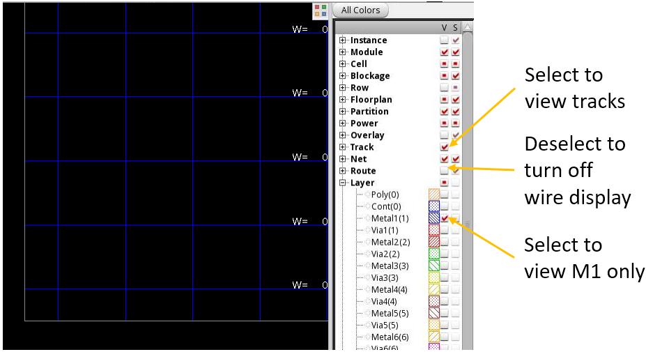
Note that the display of W= 0 does not mean that the net is to be routed with a wire of 0 width. W= 0 means that the default width is specified for the tracks, where default width is the width specified in the LEFDefaultRouteSpec in the technology library. If a non-default width is specified for the tracks, the display will show the exact width value.
To view the tracks better, you may deselect the Visibility check boxes of other object types, such as Instance, Route, and Row. You can also turn off other routing layers. For example, turn off any layers other than M1 if only M1 routing grid is to be viewed.
For a cell view that has its floorplan created in Virtuoso with floorplan but with no rows and no Width Spacing Patterns (WSPs), Innovus will insert the rows and tracks accordingly during the import process of the design.
Typically, the routing tracks for each metal routing layer have uniformed spacing, called pitch. The first horizontal track starts from the bottom and the distance between the first track and the bottom edge of the core area is called offset. These specifications are commonly found in the LEFDefaultRouteSpec constraint group in the technology library.
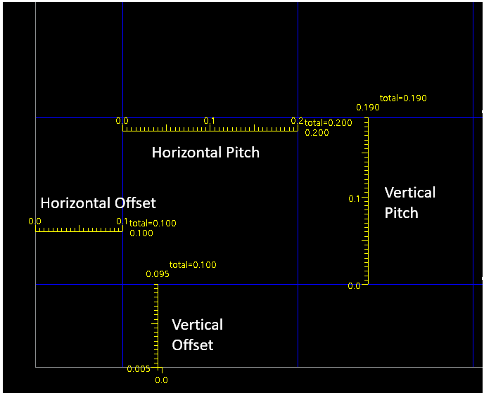
For the above example, the values are specified in the technology file as follows:
“LEFDefaultRouteSpec” nil “LEFDefaultRouteSpec”
...
routingGrids (
( horizontalPitch “M1” 0.2 )
( verticalPitch “M1” 0.19 )
( horizontalOffset “M1” 0.1 )
( verticalOffset “M1” 0.095 }
Alternatively, in the Technology LEF file, the equivalent statements are:
LAYER M1
...
PITCH 0.2 0.19 ;
OFFSET 0.1 0.095;
16.3 Guidelines for Using Innovus To Route a Design from Virtuoso
- If I/O pins are created and placed in Virtuoso and their corresponding nets are to be routed in Innovus, do not specify the placement attribute to be
NoneorUnplacedas then the router in Innovus will view them as not physically placed and will not able to route. The router will issue a message similar to the following:#WARNING (NRIG-39) NanoRoute cannot route to pin PIN/output9 of net output9 because it might be a logical pin and does not have physical shapes. To fix the problem, check the pin connection in the netlist and ensure the pin shapes exist in the floorplan.
It is recommended to update the placement attribute of I/O pins toFixed(Locked/Coveris fine too) if no adjustment of the placement location is to be done in Innovus orPlacedif adjustment is expected.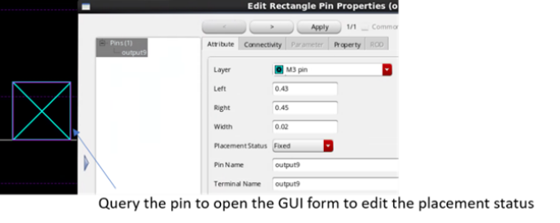
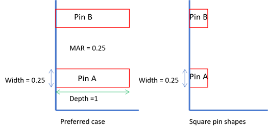
- For I/O pins created in Virtuoso, it is recommended that the depth of the pin shapes should be large enough to meet the minimum area rule (MAR), if such a rule exists. In most cases, the router in Innovus can add wires to increase the depth of pin shapes to meet the minimum area rule during the detailed routing of the whole design. However, ensuring that the pin shapes have appropriate depth upfront will ease the burden on the router and may prevent creation of DRC violations in corner cases.
- The detailed abstract of the standard cells to be routed in the design should be loaded into Innovus during design initialization (through the
init_oa_ref_libvariable), especially for good quality of routing result in the lower technology nodes.
- The Core Boundary in Innovus affects the way routing tracks are created. Refer to the Design and Core Boundary in Innovus chapter for more details of core boundary and its relationship with track creation.
-
Alignment of routing tracks with the I/O pins of the design or the standard cells are critical, especially in smaller nodes. Improper alignment may result in bad quality of result. Refer to the Track Alignment in Innovus section for more information on aligning tracks with other objects, such as the I/O pins of design and cells.
16.4 Interoperability of Routing Tracks
A higher percentage of mixed signal designs are being implemented at lower semiconductor process nodes. At these nodes, tools that are used to implement the custom portion of the mixed signal design have to adhere to certain structures for implementing the routing requirement of the design. Traditionally, place and route tools used for implementing the digital portion of mixed signal designs have had to create routes based on certain track definitions. For mixed signal designs using lower semiconductor process nodes, these two different methods of creating routes must be aligned. Otherwise, issues can crop up during the assembly of the overall design, which may require changes to the content that has already been implemented.
For lower process nodes, Virtuoso requires a Width Spacing Pattern (WSP) to be created and used when routes are created in the tool. An example of a WSP created for METAL1 in Virtuoso is given below:
dbCreateWidthSpacingPattern(cv "oax_pattern1_cv" '(((0.020 0.070)) ((0.020 0.040)) ((0.020 0.040)) ((0.020 0.040)) ((0.020 0.040)) ((0.020 0.70))) 0.0 ; Assume offset 0 from the axis and use the space in the pattern ) dbCreateWidthSpacingSnapPatternDef(cv "oax_M1WSP_cv" list("METAL1" "track") "vertical" ; direction 0.30 ; period "oax_pattern1_cv" ; default active pattern list(list("METAL1")) ; snapping layers 0.0 ; offset from PR Boundary or axis list("oax_pattern1_cv") ; list of possible patterns )
The graphical representation of the tracks defined by this WSP is shown below:
16.4.1 Supported Use Models for the Interoperability of Routing Tracks
16.4.1.1 Use Model A
In a mixed signal flow in which the custom content is created in Virtuoso and the digital content in Innovus, a user may create a WSP in Virtuoso and mark it as the active WSP to be used for implementing the digital content of the design. In this case, Innovus must read and convert the user-created, active WSP to track patterns that are used by the router in Innovus.
Note that a specific cell view may have many different WSPs. However, only the active WSP would be converted to routing track patterns in Innovus. This use model is depicted in the diagram below.
Use Model A: The active WSP is automatically converted to routing tracks in Innovus.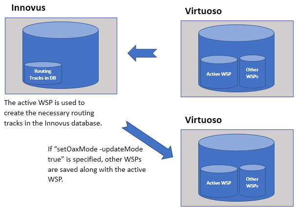
In this flow, the active WSP is directly stored in the Innovus DB as routing tracks. However, if you later use database access routines to change the routing tracks in the database, Innovus will create an additional WSP with the following naming convention:
invs_<layer_name>_wsp // WSP Name
Once the design is saved in Innovus, you can see both the original WSP as well as the Innovus-generated one.
16.4.1.2 Use Model B
In this use model, you do not create any WSP in Virtuoso or do not mark any of the WSPs as active. This use model should be used if you wish to run NanoRoute in Innovus on either a standard-cell-based block in the design or the top-level design and take the results back to Virtuoso. NanoRoute has the ability to create the most efficient routing tracks for a specific design or cell view. You can take advantage of this capability to make Innovus generate a WSP automatically based on the routing tracks in Innovus. This Innovus-generated WSP can then be used for wire editing or other applications in Virtuoso. This process is done automatically in the OpenAccess flow when saving the design.
In this flow, the track patterns in Innovus can be created using the Innovus add_tracks command, with the following two options at a minimum: -width_pitch_pattern and -keep_default_width.
The WSP created during saveDesign by Innovus will have the following naming convention:
invs_<layer_name>_wsspd // Snap Pattern Def name
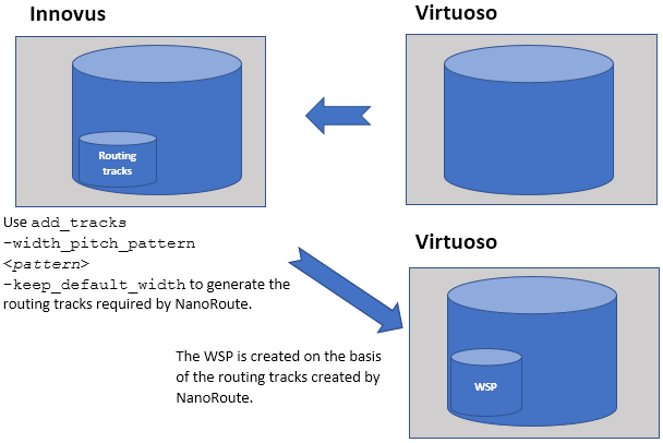
Use Model B: No active WSP exists, and Innovus routing tracks are used to create WSPs.
16.4.2 Role of add_tracks in the Interoperability of Routing Tracks
The add_tracks command is used in Innovus for creating the complex routing track patterns required in lower technology nodes.
In some lower technology nodes, specific track pattern definitions are required by the foundry so that the tool can generate the most efficient routing results for the design. It is possible to make the Innovus-generated routing tracks compatible with Virtuoso so that a WSP can be created from the routing tracks used by Innovus. If add_tracks is used in Innovus, you need to make sure that the following two options are part of the syntax for the add_tracks command because the use of these options with the add_tracks command makes the generated tracks interoperable with the WSPs in Virtuoso. The two options are-width_pitch_pattern and -keep_default_width.
The -keep_default_width parameter has no argument. However, the syntax for the -width_pitch_pattern pattern is as follows:
-width_pitch_pattern {{layer1 offset offset width width pitch pitch [width width pitch pitch]...} [{layer2 ...}]...}
When When If there is more than one WSP in the design, it is important to specify 16.4.3 Role of setOaxMode -updateMode in the Interoperability of Routing Tracks
setOaxMode is an Innovus command that controls the behavior of the Innovus tool when run in the OpenAccess mode. One of the options for this command is -updateMode false | true | auto. setOaxMode -updateMode is set to true, Innovus retains and writes back all custom objects, such as Fig-groups, Modegen cells, and so on. Therefore, if a design containing such custom objects is brought into Innovus for modifications, it would be best to set -updateMode to true.setOaxMode -updateMode is set to false, Innovus ignores the custom objects in the design. This mode is typically used when working on a digital block of a mixed signal design, where the implementation is being done using Innovus. In this situation, there are no custom objects that Innovus needs to retain.setOaxMode -updateMode true if you wish to retain the non-active WSPs as part of the design. Similarly, if WSP regions or WSP families are to be preserved in the round trip to Innovus, setOaxMode -updateMode true is required. Innovus will not recognize either of these WSP types, but will retain the information and send it back to Virtuoso.
16.5 Track Alignment in Innovus
For aligning tracks with objects such as I/O pins, several points need to be considered. These are:
16.5.1 Relationship Between Wire Width, Routing Track Pitch, and Minimum Spacing Requirement
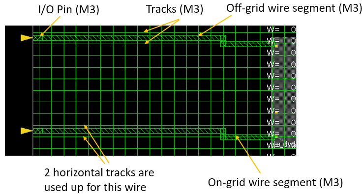
NanoRoute prefers to create routes along the routing grid with tracks being the center-line of wires. However, NanoRoute has the flexibility to create off-grid wires, where necessary. For example, an off-grid wire may be created to make a connection to an off-grid I/O pin. Nevertheless, that will mostly incur the loss of the adjacent track segment. The impact of the misalignment between certain I/O pins and routing tracks depends on the wire width, routing track pitch, and the minimum spacing requirements specified in the technology.
In the image on the left below, the routing pitch of M2 is 0.2um and the wire width of M2 is 0.08um. If the minimum spacing is 0.08, an off-grid wire with its center-line of not more than 0.04um deviation from the grid is still okay.
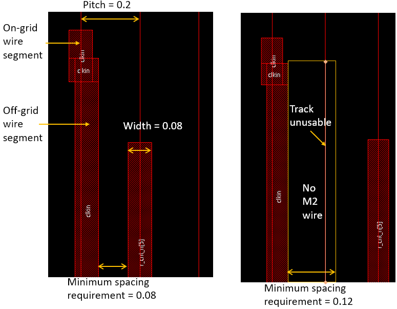
However, on certain technology nodes, it is possible that the minimum spacing requirement is the exact difference between the pitch and the wire width (0.12um in the case above). As a result, any off-grid M2 wire segment will make the area bounded by the orange box shown in the image on the right above unusable for the creation of an M2 wire. The router will not be able to use that portion of the M2 track for connections to other pins. Under such conditions, especially in a highly-dense design, the alignment of routing tracks with I/O pins and standard-cell pins becomes critical. This will be explained in detail in subsequent sections.
16.5.2 Alignment of I/O Pins with Routing Tracks
The I/O pins must be aligned with the routing tracks for optimal quality of result. The following diagram shows a sample routing result of I/O pins that are not aligned with routing tracks. In this example, the non-alignment of the pins with the tracks does not result in any DRC violation but incurs loss of adjacent routing track. However, in some other cases, non-aligned pins can create routing congestion and DRC violations due to non-optimal spacing between off-grid and on-grid wires.
In addition, some lower-technology nodes require wires to be rectangular in shape. In such cases, the non-rectangular shape of the wire above will be considered as a DRC violation.
To avoid such issues in a design imported from Virtuoso into Innovus, the designer must have the desired routing track pattern or WSP in mind if the I/O pins are to be created in Virtuoso and the pins must be aligned with these tracks (WSPs). Note that if both the routing tracks and I/O pins are generated by Innovus, there won’t be any issue because the I/O pins created by Innovus are always snapped to the routing track.
The following example shows the result of I/O pins aligning with the routing track.
The preferred routing direction of M3 is horizontal in this example. By turning on the Visibility check box for only Pref Track on the control panel, you can view and analyze tracks more easily.
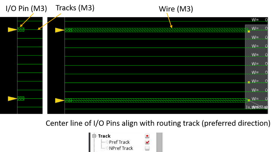
The yellow triangles in the design are symbols displayed in Innovus to help you locate the I/O pins and to determine their direction. A yellow triangle with its tip pointing in represents an input port, whereas a yellow triangle with its tip pointing out represents an output port. Bi-directional input/output ports are represented with yellow diamonds, instead of a triangles.
As the tip of the triangle is at the centerline of the rectangular pin shape, the alignment of the I/O pin with the track and can be determined easily by checking whether the tip touches the track.

Innovus also provides the check_tracks command to check for off-grid pins. Here's an example from a sample report showing off-tracks I/O pins in the design:
#Detail Summary of Off-Track Pins:
#Off Track Top Level Pin out3
#Off Track Top Level Pin out2
#Off Track Top Level Pin out16
16.5.3 Alignment of I/O Pins with Non-Uniform-Pitch Tracks in Lower Technology Nodes
In lower technology nodes, I/O pins may be placed so as to follow a specific track pattern with non-uniform spacing (or pitch). If a cell view does not contain a WSP that can be converted to routing tracks, then Innovus by default creates routing tracks with uniform pitch. This will result in misalignment between certain I/O pins and routing tracks. The image below illustrates the issue.
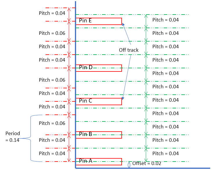
If the routing is not dense and pins are spread apart widely, the router may be able to route to the pins successfully with off-grid wires and no DRC violation. However, if the area is highly congested, routability issues may arise. In such a case, you can use the add_tracks command to specify a track pattern with non-uniform pitch. Refer to the Track pattern with non-uniform pitch subsection for more details and examples.
16.5.4 Access to I/O Pins with Double Patterning Layers in Lower Technology Nodes
For I/O pins that are assigned to metal routing layers that use double patterning, the router has to add wires of the right mask number to make a connection to the I/O pins. You can use the -mask_pattern option of the add_tracks command to specify the mask order of the routing track pattern. For example, for the following diagram, you can specify the mask order as M3 1 2 to guide the router.
Note that specifying -mask_pattern is optional as the router is able to determine the mask order automatically in most cases. Nevertheless, it is a good practice to guide the router by specifying the mask order if this piece of design information is already known.
16.5.5 Access to Standard-Cell I/O Pins in Lower Technology Nodes
In addition to the I/O pins of the design, the routing track pattern also affects the quality of the routing result on the standard-cell I/O pin connections. While creating routes to make a connection to the I/O pins of a standard cell, a router can either add a wire to the same metal layer as the I/O pins or drop a via onto the I/O pin geometries. If a standard-cell I/O pin has no or few intersections with the routing track, it may create a DRC violation or block the routes to another pin, causing an open. This kind of problem is called a standard-cell pin access issue.
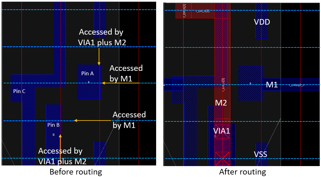
Consider the 'Before routing' image on the left hand side below. Pin B and Pin A can be accessed by the M1 wire or the VIA1 via with the routing tracks (blue dashed lines) generated at right locations. The image on the right shows one possible routing result. The router connects Pin B through VIA1 and the M2 wire and connects Pin A with the M1 wire.

To illustrate how the routing track pattern affects the routing result, the image on the left below shows the same standard cell with the routing tracks for M1 not created at the right locations. For Pin B, if the router adds M1 from the right by following either of the two horizontal tracks from the bottom, it will create a short to the other pins. As a result, Pin B will mostly be accessed only by the VIA1 via. NanoRoute can create an off-grid M1 wire to access Pin B, but this may mean the neighboring M1 track near the pin cannot be used for other nets to prevent DRC violations, such as a spacing violation. The image on the right below shows a sample routing result. The router chooses to connect Pin A with VIA1 because the router prefers to route on the grid. In this case, the routing congestion is low, so there is no DRC violation. However, if many standard cells with high-pin density are placed close to each other, poorly located routing tracks may lead to routing issues.
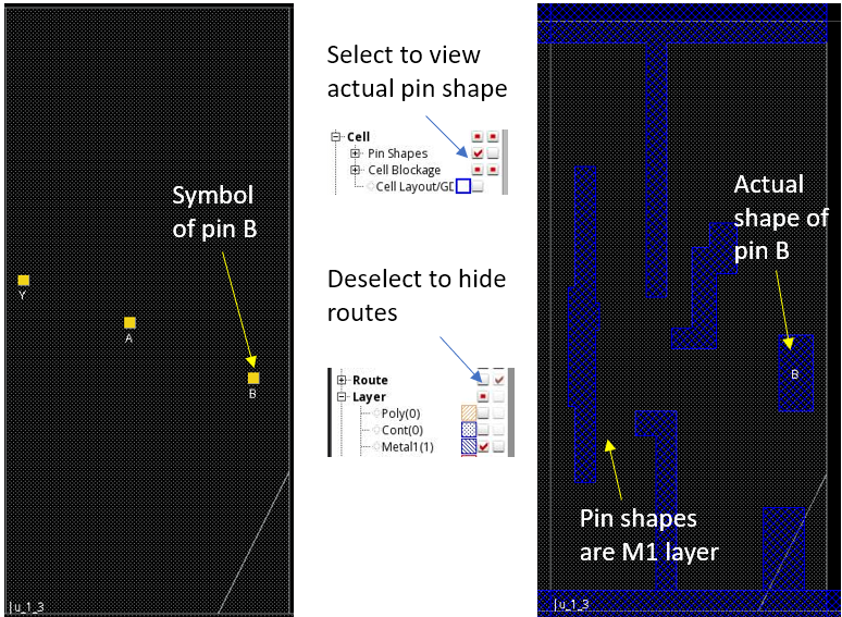
By default, Innovus does not display the pin shape of a standard cell. The yellow square(s) inside the standard cell is not a real physical object but just a symbol to indicate that there is an I/O pin. To view the actual pin shapes, select the Visibility check box of Pin Shapes on the control panel. Make sure the Visibility check box of the metal layer that the I/O pins use is also selected . For example, Visibility check box of Metal1 should be selected if the pin is of layer Metal1. If the design is routed, deselect the Visibility check box of Route so that the wires are hidden and the pin shapes can be seen more clearly.
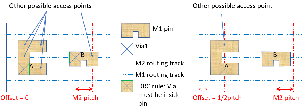
In the above case, any point where the routing tracks touch the pin shape geometries indicates a possible location for the router to insert a via to make a connection. In some nodes, there could be a design rule requirement that the vias inserted by the router must be fully inside the geometries of the I/O pin of the standard cell. In some cases, the I/O pins of these standard cells are designed in a way that the pins require routing tracks of a specific routing pitch and offset. If the routing tracks are not created with the right offset, it may become more difficult for the router to find the right solution for accessing the pins. As a result, the routing result may not optimal or the run time may increase significantly.
As an example, consider the image on the left below. If the right track pattern is created, there are five possible access points for the router to insert a via for Pin A and two possible access points for Pin B. However, if the offset is not specified correctly, resulting in the generation of poorly located routing tracks, the router would find less preferable locations to access the pins. Though it is possible to create an off-grid wire, the router either needs to spend more time to find a good solution or settle for a less optimal quality of result.
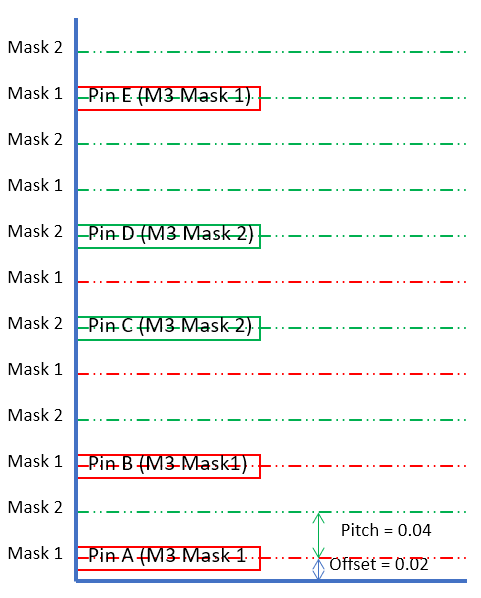
16.5.6 Access to Standard-Cell I/O Pins with Double Patterning Layers
In some lower technology nodes that use double patterning technology, the bottom few metal routing layers typically carry two masks. As most standard-cell I/O pins are implemented with one or two bottom metal routing layers, the routing tracks for these layers can also be differentiated with two different masks. When the mask pattern (or mask order) of the routing tracks are defined using the add_tracks command, ensure that the mask pattern is in the right order so that the mask number of M1 track matches the mask number of the standard cell pins.
The above diagram shows three standard cells and in each standard cell, each pin has its own mask number. Let us assume all the standard cells in this design are manually placed in Virtuoso and the cell view is loaded into Innovus. If the offset, pitch and mask pattern are specified correctly, the router in Innovus can add wires or vias with the right mask number and at the right location to access the pin easily as shown in the diagram below.
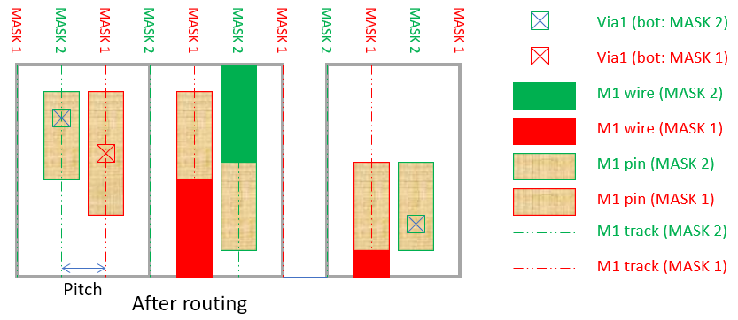
Let us assume the add_tracks command for the above case is specified correctly as follows:
add_tracks -mask_pattern {M1 1 2 ...} -offsets {M1 0 ...}
What would happen if the mask pattern is specified with the wrong order (reverse order) as follows?
add_tracks -mask_pattern {M1 2 1 ...} -offsets {M1 0 ...}
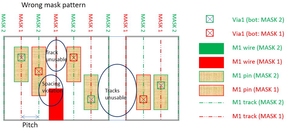
Most likely, the incorrect mask pattern specification would result in the router being unable to add wires to make connection with the pin and would restrict the router’s solution space to just via insertion for pin access. If the design rule requires the geometries of the same mask to be centered two track distance apart, it could also cause a spacing violation between the M1 pin and the M1 wire of the same mask number and make the track segments close to the pins unusable for routing.
What if the mask pattern is specified with the correct order but incorrect offset as follows?
add_tracks -mask_pattern {M1 1 2 ...} -offsets {M1 0.4 ...}
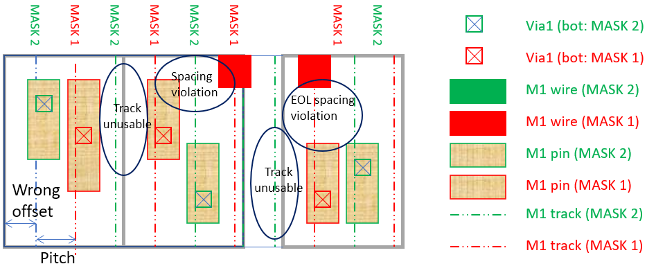
The incorrect offset specification may similarly make certain segments of tracks unusable for routing and may restrict the router’s solution space to only via insertion for pin access. It may create a spacing and End-of-Line (EOL) spacing violations between geometries of the same mask number.
To summarize, in some lower technology nodes, the routing tracks are expected to be perfectly aligned with the pins with the right mask number. This is based on the concept of “correct by construction” in a way that as far as the routes are created on-grid, the chance of achieving a good routing result is high.
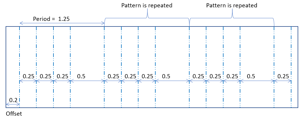
16.5.7 Track Patterns with Non-Uniform Pitch
In lower technology nodes, the designer may prefer a routing track pattern of non-uniform pitch. For example, suppose that the M4 metal routing layer has a vertical preferred routing direction and its routing track is desired to be a repeated pattern of four tracks with default wire width (specified in Tech LEF/LefDefaultRouteSpec) and non-uniform spacing values as shown in diagram below. The equivalent command in Innovus is:
add_tracks -pitch_pattern {M4 offset 0.2 {pitch 0.25 repeat 3} pitch 0.5}
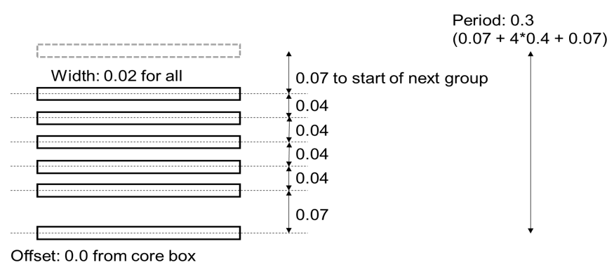
16.5.8 Track Patterns with Non-Uniform Pitch and Non-Default Width
The add_tracks command also allows you to specify routing tracks with width and pitch pattern. Consider a WSP for M3 with the offset value, wire widths and spacing requirements between wires as shown in the following diagram. The equivalent command in Innovus is:
add_tracks -width_pitch_pattern {{M3 offset 0.03 width 0.02 pitch 0.04 width 0.02 pitch 0.07 width 0.04 pitch 0.08 width 0.04 pitch 0.07}}
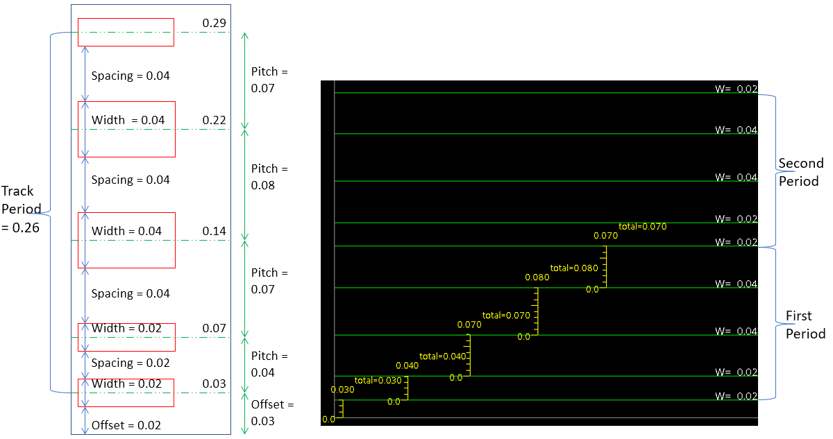
In the above example, note that:
- In the right-side image, the width values (
W = 0.02orW= 0.04) is displayed for each track. - The period offset in WSP is the distance between the bottom edges of the PRBoundary object and the first wire of the pattern. In Innovus, by default, the offset is the distance between the centerline of the first wire above the bottom edge of the Core Boundary and the bottom edge of the Core Boundary for horizontal tracks. Note that the size of the Core Boundary does not necessarily need to be the same as the size of PRBoundary object in Virtuoso. Refer to the Design and Core Boundary in Innovus chapter to understand how the Core Boundary can affect the creation of rows and routing tracks in Innovus.
- In WSP, if the spacing value is specified as the edge-to-edge mode, the spacing values at each interval should not be mistaken as the routing pitch in the
add_trackscommand. Note that the pitch is measured between the centerline of wires.