9
Extracting Parasitic Resistance (PRE)
This main focus of this chapter is on PRE for Dracula. The following areas are covered:
- “Overview of Parasitic Resistance Extraction”
- “Creating the Resistor and Resistor Terminal Layers”
- “Creating the Pad Terminal Layers”
- “Calculating Junction Resistance”
- “Redistributing Parasitic Capacitances”
- “Sample PRE Rules File”
- “Considerations for Parasitic Resistance Extraction”
- “Sample Data and Results”
- “Hierarchical PRE”
Overview of Parasitic Resistance Extraction
Parasitic Resistance Extraction (PRE) is a Dracula tool that enhances Layout Parameter Extraction (LPE) by extracting parasitic resistance created by any of the conduction layers in the layout. With LPE and PRE, you can extract resistance and capacitance parameters in the interconnect layers of the layout and generate accurate simulations for the most critical designs.
PRE works in both flat and composite modes. For information about running hierarchical PRE in composite mode, refer to the
Features of PRE include the following:
- Flexible geometric cutting of resistors, giving you control over the parasitic resistance extraction process
- Automatic generation of resistor body and terminal layers for resistance computation
- Computation of resistor values by square counting (using length and width) and sheet resistance values you provide
- Accurate automatic calculation of junction resistances, including 90-degree corners, T-shaped junctions, and cross-shaped junctions
- Pi (π) and ladder distribution of coupling and fringe capacitances involving parasitic resistor layers
- Resistor shorting and smashing to reduce the R/C network based on thresholds you supply
- Backannotation that extracts names from your schematic netlist and uses them on the extracted SPICE or CDL list
- Output of netlist in SPICE or CDL format
PRE operates in two passes. During the first pass, which is usually performed as part of the Layout Versus Schematic (LVS) check, the circuit is connected normally. During the second pass, the specified conduction layers are geometrically divided into resistor terminals regions and parasitic resistor component regions. During this pass, the circuit is reconnected to include the parasitic components in place. The conduction layer nodes split up into subnodes (the resistor terminal regions) with the parasitic resistors (resistor layer regions) placed across them. Parasitic capacitors are created after this, such that they are distributed across the subnodes. The new circuit, including all parasitic information, is output as a SPICE or CDL file.
You can backannotate the output netlist by deriving node and newly created subnode names from the original schematic netlist used in the LVS check.
The following sections describe in detail the two passes of the extraction procedure.
First PRE Pass
During the first pass, you define and connect the various active components with the CONNECT commands, which is similar to preparing for an LPE or LVS operation. The first pass retrieves the original nodal information for automatic internal layout cross-reference purposes during the second pass. The second pass generates new nodal information because of the introduction of parasitic resistors and new nodes.
During the first pass, PRE does the following:
- Backannotates to the schematic level when an LVS is performed in the first pass
- Verifies there are no LVS errors prior to performing the parasitic resistor extraction
The LVSCHK command marks the end of the first pass. If you do not need an initial LVS run, follow the CONNECT statements with the commands for the second pass.
If you want a layout-only PRE run, you do not need to include the LVSCHK command. The resulting SPICE or CDL netlist is based on layout information only.
Second PRE Pass
The second pass uses the nodal information from the first pass to reconnect the circuit. This pass can also use the first pass LVS schematic netlist for backannotation.
In the second pass, PRE does the following:
- Creates the resistor and resistor terminal layers from the specified resistive conduction layer.
- Reconnects the circuit using the created terminal layer.
- Redefines elements.
- Creates the parasitic resistor and parasitic capacitor devices.
- Generates the SPICE or CDL output file.
The following sections describe the commands you use for these steps.
Step 1: Creating the Resistor Terminal and Resistor Layers
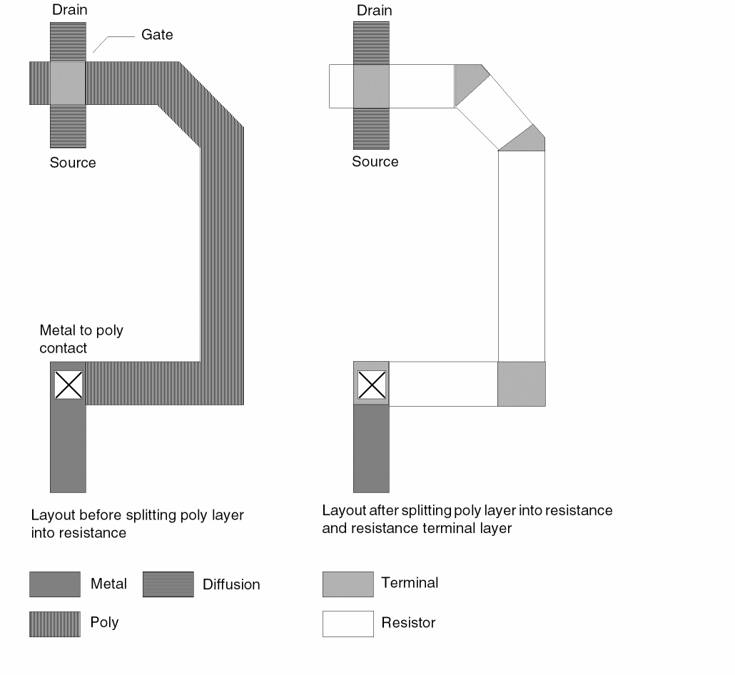
Split the trapezoids of the conduction terminal regions and create two new layers by using the CUT-TERM command. The CUT-TERM command creates a resistor body layer and a resistor terminal layer from a conduction layer and a contact layer. You can also use a series of geometric operation commands (such as SELECT and SIZE), spacing and logical operations, and the CUT command to achieve similar results. The splits are done in such a way as to isolate the regions where it makes the most sense to create parasitic resistor devices. The regions corresponding to the resistor terminal layer are treated as conduction geometries, whereas the regions corresponding to the resistor layer are treated as parasitic resistor device recognition areas connected at two terminal regions.
Resistor terminal regions are created over active devices (for example, gate areas of MOS transistors), contacts, corners of conduction lines, nonparallel geometries, wide conduction lines, and places where the width of the conduction line changes.
For more details about splitting the resistance and resistance terminal layers, refer to the section “Creating the Resistor and Resistor Terminal Layers”.
The following example shows how the conduction polysilicon (poly) layer is split into resistor and resistor terminal regions by the various commands.
Step 2: Reconnecting the Circuit
After the conduction layer is split, the circuit must be completely reconnected with the resistance terminal layer taking the place of the conduction layer.
Because contacts found in the conduction layer are still found in the resistor terminal regions, the connectivity remains the same with one exception: the parasitic resistors that approximate the resistance of the conduction layer are now in place between the terminal regions.
To reconnect the circuit, use the RCONNECT-LAYER command in the Input-Layer block. The sequence of layers corresponds to the same layers used in the CONNECT-LAYER command, substituting the resistor terminal layers for the corresponding conduction layers. RCONNECT commands in the second pass correspond to the CONNECT commands in the first connection pass, except for the substitution of the resistor terminal layers for the corresponding conduction layers.
All layers on the RCONNECT-LAYER sequence must have nodal information prior to executing the RCONNECT commands. The connection process during the first pass provides some of the information. Use the STAMP command to copy nodal information from the conduction layers that were split into the resistor terminal layers. After reconnection, all layers on the RCONNECT-LAYER sequence get new nodal information, reflecting the subnodes created (the split resistor terminals).
New subnode numbers or names are generated from the original node numbers or from the original node text if you do not request backannotation. The new subnode number or name is generated by concatenating the original number or name with a delimiter and a new number. The second number is chosen to differentiate the new node numbers and names. The sample SPICE output files in this chapter show examples of new node names and numbers.
Step 3: Creating Parasitic Resistors and Capacitors from the Resistor Layers
You define parasitic resistor devices for a given resistor layer by using the PARASITIC RES command. This command uses the fully created resistor and resistor terminal layers as parameters. You must use an ATTRIBUTE RES command associated with the PARASITIC RES to provide the sheet resistivity. The resistances can then be derived from the geometries of the resistor layers, the sheet resistance value provided, and the resistor terminal pairs from the geometries of the resistance terminal layer.
If you want parasitic capacitors, use the PARASITIC CAP and ATTRIBUTE CAP commands after creating the parasitic resistor devices.
When creating the parasitic capacitors, consider capacitances to both the resistor and the resistor terminal layers, now taking the place of the original conduction layer. Parasitic capacitances associated with the resistance layers are automatically redistributed to the resistor terminals. For more information about parasitic capacitances, refer to the Redistributing Parasitic Capacitances section in this chapter. If you specify the CUT-TERM command, Dracula automatically computes junctions of the resistance terminals. Refer to the Calculating Junction Resistance section in this chapter.
Step 4: Redefining Elements
After replacing a conduction layer with a resistor and resistor terminal layer, you must redefine elements defined with this conduction layer during the first pass, using the new resistor terminal for the second pass. For example, if the poly layer is split into a resistance layer PRES and a terminal layer PTRM, define MOS devices again during the second pass using the PTRM layer in place of the poly layer. The following commands might be used for such a purpose:
; Pass one MOS element definition:
     . . .
     ELEMENT  MOS[N]  NGATE  POLY  NSD  PWELL
     ELEMENT  MOS[P]  PGATE  POLY  PSD   NSUB
     . . .
; Pass two MOS element definition:
     . . .
     ELEMENT  MOS[N]  NGATE  PTRM  NSD  PWELL
     ELEMENT  MOS[P]  PGATE  PTRM  PSD   NSUB
     . . .
Step 5: Generating the SPICE or CDL Output File
Use the LPESELECT command to create the SPICE or CDL netlist file.
To short small resistors created by the cutting of parasitic resistance, specify a threshold with the LPESELECT RES command. The terminals of resistors having less or equal resistance than the threshold are shorted. You can use the ATTRIBUTE RES command to merge resistors that are too small.
Obtain new node names by concatenating a delimiter and a subnode number to the original node name or number. Use the SUBNODE-DELIMITER command to override the default delimiter, a colon (:) that is used in the concatenation. Request backannotation with the S option. With backannotation, node names from the original netlist are used instead of node numbers to create the new node names.
Creating the Resistor and Resistor Terminal Layers
The two basic entities in layout circuit extractions are geometries representing devices and geometries representing conductive terminals or nodes. In cutting parasitic resistors, polygons (or the resistive conduction layers) must be partitioned into the following:
- Rectangular areas (as much as possible) corresponding to resistor devices
- Rectangles or polygons corresponding to resistor terminal regions. Resistor terminal regions act as conduction layer nodes that connect together the two-terminal parasitic resistors and other devices.
You can cut the resistor and resistor terminal layers in two ways: use the CUT-TERM command or use a series of commands. Using the CUT-TERM command is the preferred method for new rules files because it requires fewer commands and produces more accurate results.
Using the CUT-TERM Command
The CUT-TERM command cuts parasitic resistors as follows:
- Cuts contact regions from the resistor layer.
- Cuts junction areas from the resistor layer. It can cut 90-degree corner junctions, T-junctions, and cross-shaped junctions.
- Cuts long geometry strips into smaller segments. A long strip geometry is more accurately represented as a series of R/C lumped circuits.
To learn how to create resistor and resistor terminal layers or for a list of the commands CUT-TERM replaces, refer to the CUT-TERM section in Chapter 13 of this manual.
Using a Command Sequence
You can use combinations of Dracula spacing and logical commands plus SIZE, SELECT and CUT commands to cut the layers, then save the result as the resistor layer and the resistor terminal layer. The conduction layer polygons can be split in a variety of ways. In general, the splitting process should follow these rules:
-
The connection between different layers can only be done through contacts at conduction nodes.
Form resistor terminal regions around contacts involving the specified conduction layer. -
Resistors are two-terminal devices.
Form resistor terminals at all branching corners (corners of T-shaped polygons, Y-shaped polygons, and so forth). -
All resistors must be rectangles.
Cut non-rectangular resistors into rectangles to get better accuracy in the parasitic resistance calculations. -
Terminals for active devices must be connected to nodes.
Include the MOS gate areas made out of a specified resistive conduction layer, such as poly, as resistor terminals.
Creating the Pad Terminal Layers
The basic parts of the layout circuit extractions are geometries representing devices and conductive terminals or nodes. You must do the following when using the PAD-LAYER command:
- Define the pad terminals in the Input-Layer block following the RCONNECT-LAYER command.
- Specify one PAD-LAYER command in the rules file for PRE or HPRE if it applies all cut-term layers. Otherwise, list each pad layer for its effected layers respectively. If you do not specify the affected cut-term layers, PAD-LAYER affects all cut-term layers.
- Input the pad layer from the input database or a derived layer.
PRE or HPRE performs the LOGICAL AND operation on the CUT-TERM input-conduction layer and on the pad layer defined by the PAD-LAYER command in order to form extra terminals automatically.
You can specify multiple PAD-LAYER commands with a set of affected cut-term layers specified for each pad-layer in the same rules file.
Use one of the following methods to create pad layers:
-
Generate a ring geometry (that is, on the boundary) as the pad layer (HPRE). This method does not work for hierarchical runs.
PAD-LAYER = PPAD
...
SIZE BULK BY -0.1 TBULK
NOT BULK TBULK PPAD
- Use the passivation layer as the PAD-LAYER.
-
Use the LABEL command. For example, attach text to the METAL layer located near the boundary.
PAD-LAYER = PPAD
....
SELECT METAL LABEL[R] ? PPAD
-
Use the output of the PIN-TEXT-LAYER command as the pad layer.
PIN-TEXT-LAYER = pinlay 5
PAD-LAYER = pinlay
Examples
The following example shows the location and syntax of the PAD-LAYER command in the Input-Layer block of the rules file.
*INPUT-LAYER
;
PWELL = 1                   ;PWELL layer
ACTIVE = 2                  ;All active diffusion
POLY = 3                    ;Polysilicon
PDIFF = 4                   ;P+ implant
CONT = 5                    ;All metal contacts
MET = 6    TEXT=6
SUBSTRATE = BULK 63         ;BULK used for reverse field
;
CONNECT-LAY  = NSUB  PWELL  PSD  NSD  POLY  MET
;
RCONNECT-LAY = NSUB PWELL PSD NSD PTRM MET
;
PAD-LAYER = VAPOX
*END
The following example uses multiple PAD-LAYER commands. You can specify a set of affected cut-term layers for each PAD-LAYER command.
.
.
CONNECT-LAY = NSUB PWELL PSD NSD POLY MET
RCONNECT-LAY = NSUB PWELL PSD NSD PTRM MTRM
.
.
PAD-LAYER = PAD, POLY
PAD-LAYER = VAPOZ, MET
.
.
CUT-TERM MET CONT MRES MTRM
CUT-TERM POLY CONT PRES PTRM
Error Conditions
The following error conditions can occur when you use the PAD-LAYER command.
- If you do not specify a pad layer in the rules file for a PRE or HPRE job, PDRACULA reports an error message in the .log file.
- If you do not select a pad terminal layer, the UPDPAD module reports a warning message in the .log file and randomly picks a subnode terminal for the pad.
- If you select multiple pad terminals for the same node but do not specify the MULTI-PIN-FILE command, PRE shorts the terminals together.
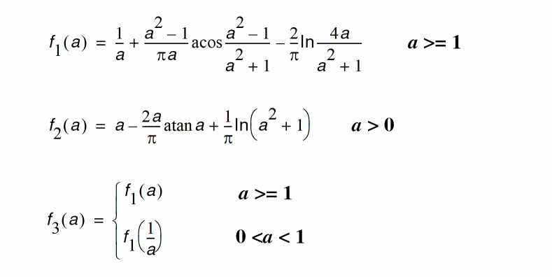
Calculating Junction Resistance
Resistance layer geometries must have two terminals. Single-terminal resistance regions are discarded. Rectangular resistance layer geometries, which provide the most accurate resistance calculation, are preferred.
The CUT-TERM command cuts junction regions from the original resistance layer and treats them as terminals. To improve the accuracy of the resistance extraction results, the resistances associated with junction regions are calculated by the following models for corner junctions, T-shaped junctions, and cross-shaped junctions:
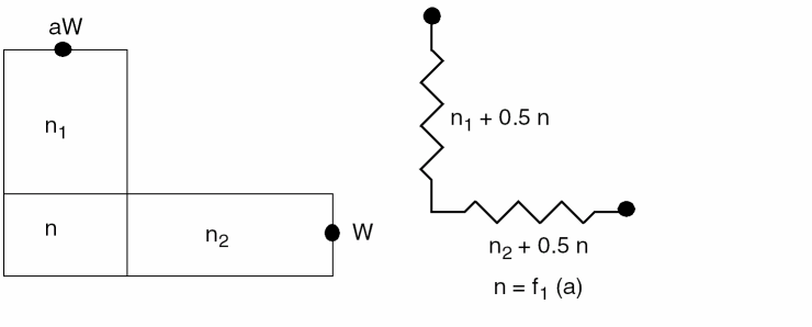
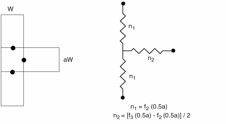
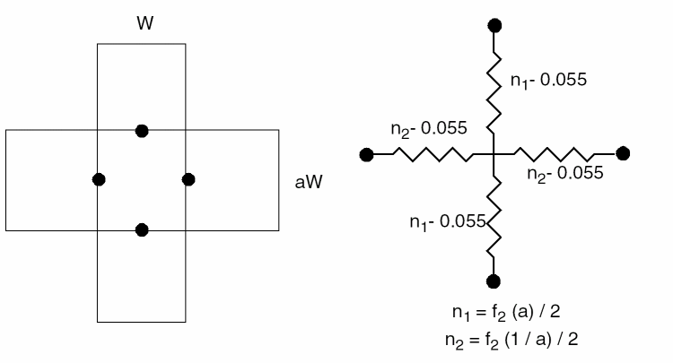
The following equations express the functions f1, f2, and f3.
Redistributing Parasitic Capacitances
Define parasitic capacitances only after the introduction of the parasitic resistors so that you take into account the new subnodes.
The parasitic capacitances can be categorized into the following types.
A node corresponds to a connected set of conduction layer geometries, or resistor terminals, or both.
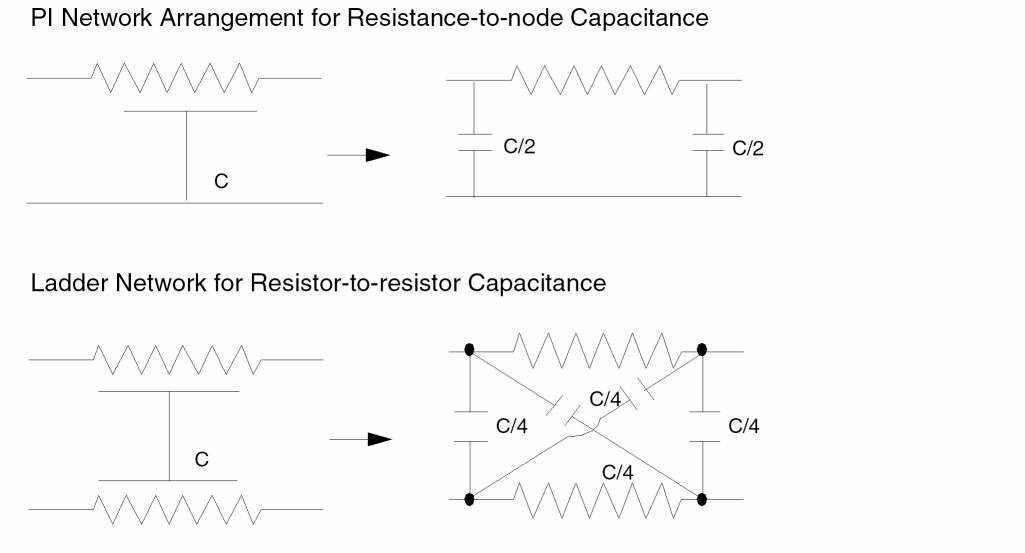
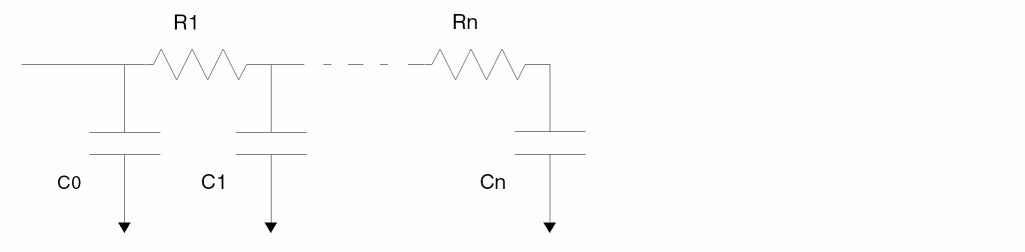
Treat internodal capacitances the same as in LPE. Lump and divide distributed capacitances computed along regions forming resistors as shown in the following two illustrations.
Because creating the parasitic resistor elements involves splitting a conduction layer into the resistor elements and the resistor terminals, you need to consider additional parasitic capacitances with the creation of parasitic resistors. The following is an example of a single-metal CMOS process. The layers from the top surface of the die to the bottom are
Metal Poly NSD (N - diffusion) PSD (P - diffusion) P-Well, N-Sub (Substrate)
The capacitances for these layers (without creating parasitic resistors) might be the following:
Metal to NSD Metal to PSD Metal to P-Well Metal to Nsub Poly to Metal Poly to P-Well Poly to N-Sub
If the poly layer is used to extract parasitic resistors, then it is split into the resistor layer PRES and the resistor terminal layer PTRM. When you write the rules file to generate parasitic capacitances, these two new layers have to be considered instead of the poly layer. The new capacitances to be calculated are the following:
Metal to NSD Metal to PSD Metal to P-Well Metal to Nsub
PRE automatically splits the total resistor-to-node capacitances (PRES to Metal, PRES to P-Well, PRES to N-Sub) into two halves and connects them to the two endpoints of the resistor terminals in the form of a PI network.
Although fringe resistor-to-resistor capacitances are not considered in the previous example, the same consideration of the split layers applies.
Sample PRE Rules File
The following rules file shows a typical command sequence for an LVS check followed by PRE operations that include parasitic resistance extraction. Many of the commands in this file correspond to the commands needed for a normal LVS check.
;***************************************************
;*******   SI-GATE CMOS INPUT FILE FOR LPE  ********
;*******   PARASITIC RESISTANCE EXTRACTION  ********
;*******              sample.com            ********
;
*DESCRIPTION
 PRIMARY = STRAIGHT_GEO     ;Top structure name
 SYSTEM = GDS2              ;System that data came from
 INDISK = STREAM.OUT        ;File on disk where data is stored
 OUTDISK = SAMPLE           ;File where output data is stored
 SCALE = .001 MICRON        ;1 database unit is equal to .001 micron
 RESOLUTION = .25 MICRON    ;Smallest increment used in DRACULA
 MODE = EXEC NO             ;Job is not be submitted automatically
 BATCH-QUEUE = FAST         ;Job is entering the FAST queue
 PRINTFILE = SAMPLE         ;Specify prefix for output files
 PROGRAM-DIR = usr1/dracula/bin
                            ;Path for DRACULA to find executables
;
DIODESEQ = A1 P1            ;Spice parameter sequence
SCHEMATIC = LVSLOGIC        ;Compiled schematic name to be used
;---------------------------------------------------------
SUBNODE-DEL = ":"           ; Subnode delimiter command
;---------------------------------------------------------
MODEL = MOS[N],N MOS[P],P DIODE[N],N DIODE[P],P
UNIT = CAPACITANCE,PF AREA,U PERIMETER,M RESISTANCE,K
*END
*INPUT-LAYER
;
 PWELL = 1             ;PWELL layer
 ACTIVE = 2            ;All active diffusion
 POLY = 3              ;Polysilicon
 PDIFF = 4             ;P+ implant
 CONT = 5              ;All metal contacts
 MET = 6 TEXT=6
 SUBSTRATE = BULK 63   ;BULK used for reverse field
;
 CONNECT-LAY  = NSUB  PWELL  PSD  NSD  POLY  MET
;
;
;
;----------------------------------------------------------
RCONNECT-LAY = NSUB PWELL PSD NSD PTRM MET
;This command establishes the layers that are involved
;when the layout circuit is reconnected by the RCONNECT
;commands given when the parasitic resistance is extracted.
;The layers shown here are the same as the CONNECT-LAY command
;except that the POLY layer has been substituted by the PTRM
;layer, corresponding to the resistor terminal layer.
;
PAD-LAYER = VAPOX
;----------------------------------------------------------
*END
*OPERATION
;
;*******************************************************
;*******          DO REGULAR LVS CHECK           *******
;*******************************************************
;
AND  ACTIVE  PDIF  PDIF       ;All P+ active regions
 NOT  ACTIVE  PDIF NDIF       ;All N+ active regions
 AND  POLY  NDIF  NGATE       ;Create all N-channel gates
 AND  POLY  PDIF PGATE        ;Create all P-channel gates
 NOT  NDIF  NGATE  NSD        ;Create all N-channel source/drains
 NOT  PDIF  PGATE  PSD        ;Create all P-channel source/drains
 NOT  BULK  PWELL  NSUB       ;Create N-substrate area
 AND  PSD  PWELL  PTAP        ;Create PWELL taps for vss
 AND  NSD  NSUB NTAP          ;Create NSUB taps for vdd
;
 CONNECT MET POLY BY CONT     ;Connect the various conduction
 CONNECT MET PSD BY CONT      ;layers through the proper
 CONNECT MET NSD BY CONT      ;contacts.
 CONNECT PSD PWELL BY PTAP    ;Connect substrate and P well
 CONNECT NSD NSUB BY NTAP     ;region through proper taps.
;
 ELEMENT MOS[N] NGATE POLY NSD PWELL ;Define N-Channel MOS
;                             ;transistors.
 ELEMENT MOS[P] PGATE POLY PSD NSUB  ;Define P-Channel MOS
;                             ;transistors.
;
LVSCHK[C]
;
;
;
;
;
;
;
***************************************************
;Here begins the second pass - which performs the *
;parasitic resistor extraction from the Poly layer*
;**************************************************
;
;********************************************
;*****   CUT RESISTORS ON POLY LAYER   ******
;********************************************
;
;Cutting Resistor Terminal Areas around Contacts
;
 OR   NGATE  PGATE  GATE   ;GATE gets all gate layer geometries.
 CUT-TERM POLY CONT PRES PTRM GATE
;                          ;GATE is T_DEV
;
;PRES now has the geometries corresponding to the Poly parasitic
;resistors and PTRM has the geometries corresponding to the Poly
;resistor terminals.
;*****************************************************
;*****  RE-CONNECT WITH PARASITIC RESISTANCE CUT  ****
;*****************************************************
;
 STAMP PTRM BY POLY   ;Get original nodal information
;                     ;from the Poly layer stamped
;                     ;into the resistor terminals.
;
;---------------------------------------------------------
;Establish new connects i.e., reconnect the circuit using
;the Poly resistor terminal layer, PTRM, instead of the
;Poly conduction layer.
 RCONNECT  MET  PTRM  BY  CONT
 RCONNECT  MET  PSD  BY  CONT
 RCONNECT  MET  NSD  BY  CONT
 RCONNECT  PSD  PWELL  BY  PTAP
 RCONNECT  NSD  NSUB  BY  NTAP
;---------------------------------------------------------
;With the Parasitic Resistors created and inserted into
;the circuit, the other parasitic devices are handled.
;
;
;
;*****************************************************
;*****          CREATE PARASITIC DIODES          *****
;*****************************************************
;
 AND  NSD  PWELL  NDIO   ;N+ Diode minus taps
 AND  PSD  NSUB   PDIO   ;P+ Diode minus taps
;
;
;
;
;
;*****************************************************
;*****       CREATE PARASITIC CAPACITANCES       *****
;*****************************************************
;!!!!!!! Note the splitting of parasitic capacitances !!!!!!!


 AND  MET  PTRM MPOLY        ;Metal to Poly Terminal Cap
 AND  MET  PRES  MPOLYR      ;Metal to Poly Resistor Cap
;
 NOT  MET  POLY  METNP       ;Create Metal with no Poly layer
 AND  METNP  NSD  MNSD       ;Metal to N+ Diffusion Cap
 AND  METNP  PSD  MPSD       ;Metal to P+ Diffusion Cap
;
 NOT  MET  MPOLY  M0        ;Prepare for PWELL and NSUB Caps
 NOT  M0  MPOLYR   M1       ;Remove all other Cap values
 NOT  M1  MNSD  M2
 NOT  M2  MPSD  M3
 AND  M3  PWELL MWELL       ;Metal to PWELL cap
 AND  M3  NSUB  MSUB        ;Metal to NSUB cap
;
 NOT  PTRM  GATE  PTRM1     ;Remove gate from interconnect
 AND  PTRM1  PWELL  POWELL  ;POLY interconnect to PWELL cap 1
 AND  PRES  PWELL  POWELR   ;POLY interconnect to PWELL cap 2
 AND  PTRM1  NSUB  POSUB    ;POLY interconnect to NSUB cap 1
 AND  PRES  NSUB  POSUBR    ;POLY interconnect to NSUB cap 2
;
;************************************************
;****  DECLARE ELEMENT AND PARASITIC DEVICES ****
;************************************************
;
 ELEMENT MOS[N] NGATE PTRM NSD PWELL ;Redefine elements with poly
 ELEMENT MOS[P] PGATE PTRM PSD NSUB  ;terminal layer PTRM instead
;                                    ;of POLY layer.
 PARASITIC DIO[N] NDIO PWELL NDIO    ;N+ Diode to PWELL
 PARASITIC DIO[P] PDIO PDIO NSUB     ;P+ Diode to SUBSTRATE
;
 PARASITIC  RES[P]  PRES  PTRM       ;POLY interconnect resistor
 ATTRIBUTE  RES[P] 0.01              ;Kohms per square
; Note that the above command indicates that the PRES layer
; corresponds to the resistance layer. This tells Dracula
; that any capacitances to these layers should be split
; according to the Pi or ladder network form.
;
;#### Capacitance attributes are in pf per unit area, as
;#### indicated in the UNIT command
;
;!!!! Parasitic Capacitors involving parasitic resistance  !!!!!
;!!!! layer and parasitic terminal resistor layer.         !!!!!
;!!!!                                                      !!!!!
;!!!! Note that capacitances involving parasitic           !!!!!
;!!!! poly resistor devices (PRES)  are automatically      !!!!!
;!!!! split in half and placed across the two ends of the  !!!!!
;!!!! resistors.                                           !!!!!
;
 PARASITIC CAP[A1] MPOLY MET PTRM   ;Capacitor from METAL layer
 ATTRIBUTE CAP[A1] 0.000025         ;to POLY resistor terminal.
 PARASITIC CAP[A2] MPOLYR MET PRES  ;METAL to POLY resistor
 ATTRIBUTE CAP[A2] 0.000025         ;capacitor.
;
 PARASITIC CAP[B] MNSD MET NSD      ;METAL to N+ capacitor
 ATTRIBUTE CAP[B] 0.000025
 PARASITIC CAP[C] MPSD MET PSD      ;METAL to P+ capacitor
 ATTRIBUTE CAP[C] 0.000025
;
 PARASITIC CAP[D] MWELL MET PWELL   ;METAL to PWELL capacitor
 ATTRIBUTE CAP[D] 0.000025
 PARASITIC CAP[E] MSUB MET NSUB     ;METAL to SUBSTRATE
 ATTRIBUTE CAP[E] 0.000025          ;capacitor.
;
 PARASITIC CAP[F1] POWELL PTRM1 PWELL;POLY to PWELL capacitor 1
 ATTRIBUTE CAP[F1] 0.000075
 PARASITIC CAP[F2] POWELR PRES PWELL ;POLY to PWELL capacitor 2
 ATTRIBUTE CAP[F2] 0.000075
;
 PARASITIC CAP[G1] POSUB PTRM1 NSUB  ;POLY to SUBSTRATE cap 1
 ATTRIBUTE CAP[G1] 0.000075
 PARASITIC CAP[G2] POSUBR PRES NSUB  ;POLY to SUBSTRATE cap 2
 ATTRIBUTE CAP[G2] 0.00007
;
;
;;*******************************************
;*****   DEFINE FRINGE CAPACITANCE     *****
;*******************************************
 PARASITIC CAP[MF] MET  MET  MET  ; MET fringe capacitance
 ATTRIBUTE CAP[MF] 5.0 0.00001
;
;!!! Note cut-term conduction layer’s fringe capacitance !!!!
;!!! use one FRINGE[R] command to define it              !!!
;
 FRINGE[R] CAP[PF] PTRM  PRE      ; POLY fringe capacitance
 ATTRIBUTE CAP[PF] 5.0 0.00002
;
;*******************************************
;*****        OUTPUT SPICE FILE        *****
;*******************************************
;
;!!!!  Note that the [S] option below indicates !!!!
;!!!!  back-annotation to the output netlist.   !!!!
;
 LPESELECT[S] MOS &               ;Output MOS transistors
 LPESELECT[S] DIO &               ;Output diodes
 LPESELECT[S] CAP GT 0.0 &        ;Output capacitors
;---------------------------------------------------------
 LPESELECT[S] RES GT 0.001 OUTPUT SPICE  ;Output resistances
                                         ;above .001 Kohms were
                                         ;indicated in the units
                                         ;command.
;---------------------------------------------------------
*END
Considerations for Parasitic Resistance Extraction
Parasitic resistance extraction (PRE) depends on geometry and method of formation. In defining parasitic resistances, consider the following:
- Because wider poly provides a reduced resistance contribution for a given length, we recommend a value of three to five times the minimum poly width as the upper limit for the MAXWIDTH parameter in the CUT-TERM command. Take into consideration the layout aspects of the resistive layer because the resistance contribution is dependent on sheet resistance and length, as well as the width of the geometries.
- Because parasitic resistance extraction is dependent on the shape of the geometries and the method of extraction, some resistances yield only approximations, rather than accurate values.
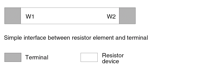
The following examples illustrate how the interface between the resistor device geometries and the resistor terminal geometries affects the resistance computation.
The calculation of a trapezoidal resistor is determined by the widths W1 and W2 of the endpoints of the resistor.
R = r * L/W
W = (W1 + W2) / 2
L = Area / W
When the resistor terminals cleanly touch the resistor element endpoints, as in the following figure, W1 and W2 both are equal to W; that is, the width of the resistor layer and the area are easily determined.
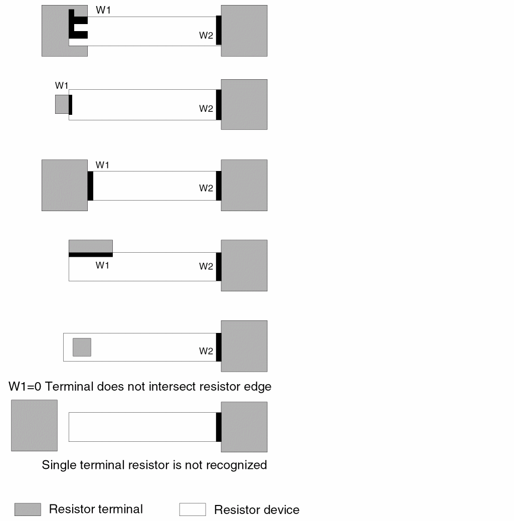
The following examples indicate the computed values for W1 and W2 when the resistor terminal geometries abut the resistor elements in special ways. For these cases, the width on a given side is determined by the edge of the resistor geometry along its intersection with the resistor terminal. If the resistor geometry fully encloses the resistor terminal, the width for that terminal is 0. The full area of the resistor regions computes L.
The widths W1 and W2 are shown with the thicker lines.
Sample Data and Results
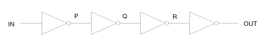
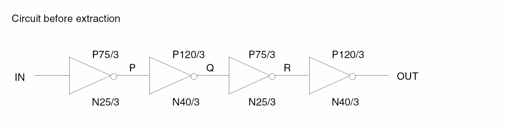
The following schematic and netlist represent an example of a four-inverter circuit given as input.
Example Input SPICE/CDL File
*.GLOBAL VDD,VSS
*
.SUBCKT INV1 Z / A
* INVERTER
MP1 Z A VDD VDD P WP=75 LP=3
MN1 Z A VSS VSS N WN=25 LN=3
.ENDS INV1
*
.SUBCKT INV2 Z / A
* INVERTER
MP1 Z A VDD VDD P WP=120 LP=3
MN1 Z A VSS VSS N WN=40 LN=3
.ENDS INV2
*
*
.SUBCKT SAMPLE OUT / IN
X1 P IN /INV1
X2 Q P /INV2
X3 R Q /INV1
X4 OUT R /INV2
.ENDS SAMPLE
After parasitic resistance extraction, the circuit is shown by the figure and the output SPICE file that follows. Single nodes often translate into many parasitic resistors and capacitors because the number of terminals and parasitic resistors generated along a path relates to the number of bends, contacts, gates, multiway branches, and other such aspects of the layout. The output SPICE file was generated with backannotation enabled so that it reflects the signal names specified in the SPICE input file.
Example Output SPICE File
*
* ECAD/LPE SPICE FILE : SPICE
* DATE : 28-AUG-85
*
******
******  MOS XTOR    PARAMETERS FROM : 7MOSXREF
******
*
*.GLOBAL   VDD  VSS
*
.SUBCKT SPICE  OUT  IN
*
******
******CORNER ADJUSTMENT FACTOR =  0.0000000
******
*
MP1X1      P IN:3  VDD VDD P   L=3.00M   W=75.00M
MN1X1      P IN:2  VSS VSS N   L=3.00M   W=25.00M
MP1X2      Q P:10  VDD VDD P   L=3.00M   W=120.00M
MN1X2      Q P:9   VSS VSS N   L=3.00M   W=40.00M
MP1X3      R:3 Q:2 VDD VDD P   L=3.00M   W=75.00M
MN1X3      R:3 Q:1 VSS VSS N   L=3.00M   W=25.00M
MP1X4      OUT R:9 VDD VDD P   L=3.00M   W=120.00M
MN1X4      OUT R:8 VSS VSS N   L=3.00M   W=40.00M
*
*----- TOTAL # OF MOS TRANSISTORS FOUND : 8
*-----                        COMMENTED : 0
*
******
******   DIODE    PARAMETERS FROM:7DIOXMER
******
*
D18   P VDD P    364.50U  195.00M
D10   VSS P N    164.50U   95.00M
D20   OUT VDD P  544.50U  285.00M
D12   VSS OUT N  224.50U  125.00M
D22   Q VDD P    544.50U  285.00M
D14   VSS Q N    224.50U  125.00M
D24   R:3 VDD P  364.50U  195.00M
D16   VSS R:3 N  164.50U   95.00M
*
*----- TOTAL # OF DIODES FOUND :8
*-----               COMMENTED :0

*******
****** CAPACITORS  PARAMETERS FROM:7CAPXMER
******
*
 C1   P     VSS  1.28000E-02PF
 C2   P:1   VSS  5.71750E-02PF
 C3   P:2   VSS  5.38625E-02PF
 C4   P:3   VSS  7.87875E-02PF
 C5   R     VSS  5.71750E-02PF
 C6   R:1   VSS  5.38625E-02PF
 C7   VDD   VSS  5.64625E-01PF
 C8   OUT   VSS  3.22750E-02PF
 C9   R:2   VSS  3.97625E-02PF
 C10  P:4   VSS  3.50750E-02PF
 C11  Q     VSS  9.36750E-02PF
 C12  R:3   VSS  1.28000E-02PF
 C13  IN    VSS  6.75000E-04PF
 C14  N:1   VSS  6.75000E-04PF
 C15  R:4   VSS  6.75000E-04PF
 C16  R:5   VSS  9.75000E-04PF
 C17  R:6   VSS  6.75000E-04PF
 C18  R:7   VSS  6.75000E-04PF
 C19  R:8   VSS  3.00000E-04PF
 C20  R:9   VSS  3.00000E-04PF
 C21  R:10  VSS  9.75000E-04PF
 C22  P:5   VSS  8.25000E-04PF
 C23  P:6   VSS  6.75000E-04PF
 C24  P:7   VSS  8.25000E-04PF
 C25  R:11  VSS  1.05000E-03PF
 C26  R:12  VSS  6.75000E-04PF
 C27  R:13  VSS  1.05000E-03PF
 C28  P:8   VSS  6.75000E-04PF
 C29  P:9   VSS  3.00000E-04PF
 C30  P:10  VSS  3.00000E-04PF
 C31  R:14  VSS  6.75000E-04PF
*
*----- TOTAL # OF CAPS FOUND : 31
*-----             COMMENTED :  0

******
******RESISTORS  PARAMETERS FROM:7RESPREF
******

 R27  IN    IN:1  1.70333E00K
 R30  IN:1  IN:2  1.29167E-01K
 R31  IN:2  IN:3  1.80833E-01K
 R32  P     P:1   3.11000E00K
 R33  P:1   P:2   3.38333E00K
 R35  P:2   P:3   3.03333E00K
 R37  R     R:4   2.61667E00K
 R38  R     R:1   3.38333E00K
 R40  R:1   R:5   3.13167E00K
 R41  R:4   R:7   1.72000E00K
 R42  R:5   R:10  2.34750E00K
 R44  R:6   R:7   1.27333E00K
 R46  R:6   R:8   1.51667E-01K
 R47  R:8   R:9   9.00000E-02K
 R49  R:2   R:10  7.50000E-02K
 R51  P:3   P:6   1.20000E-01K
 R53  P:5   P:6   9.00000E-02K
 R54  P:5   P:7   3.47000E00K
 R55  P:4   P:7   8.33333E-02K
 R58  R:2   R:11  7.83333E-02K
 R59  R:11  R:13  1.17250E00K
 R60  R:12  R:13  1.11500E00K
 R61  R:12  R:14  5.10000E-01K
 R63  P:4   P:8   5.03333E-01K
 R64  P:8   P:9   1.51667E-01K
 R66  P:9   P:10  9.00000E-02K
 R67  Q:1   Q:2   1.80833E-01K
 R68  R:3   R:14  4.13333E-01K
 R69  Q     Q:2   2.06667E-01K
*
*-----  TOTAL # OF RESISTORS FOUND :   29
*-----                   COMMENTED :    0
*
 .ENDS
Hierarchical PRE
Composite mode PRE extracts the designed and parasitic devices from the composite plane. Like flat mode PRE, HPRE generates a SPICE file with back annotation to the schematic if you are also running LVS as part of the job. HPRE generates a SPICE file with layout information only if you are not running LVS as part of the job.
The difference between PRE and HPRE is that when you run HPRE in composite mode, the HPRE program includes interconnection between instances or placements. Because of this, the format HPRE generates is not the same as flat SPICE.
For more information on running HPRE, see “
SPF File Overview
The Standard Parasitic File (SPF) lists extracted electrical data for a design created by Place and Route tools such as Block Ensemble, Cell Ensemble, and Gate Ensemble. This extracted data consists of placed and interconnected cell instances.
The SPF file can have one of two formats: detailed SPF (DSPF) format or reduced SPF (RSPF) format. Embedded in each format are two circuit level models, each with different degrees of complexity and accuracy, that represent the physical design.
DSPF Format
The DSPF format contains complete extracted circuit information, including designed and parasitic devices. Circuit simulators can use DSPF for comprehensive simulation, and timing simulators can use DSPF for delay analysis. DSPF also lists circuit-level debugging information so you can identify parasitic layout components and study their effects.
DSPF has two sections: a net section and an instance section. The net section consists of a series of net description blocks. Each net description block corresponds to a net in the physical design. A net description block begins with a net statement followed by pins, instance pins, subnodes, and parasitic resistor/capacitor (R/C) components that characterize the electrical behavior of the net. The instance section consists of a series of SPICE instance statements. SPICE instance statements begin with an X.
The DSPF format is as generic and as much like SPICE as possible. While native SPICE statements describe the R/C sections, some nonnative SPICE statements complete the net descriptions. These nonnative SPICE statements start with the notation “*|” to differentiate them from native SPICE statements.
Each file consists of hierarchical cells and interconnects only. When the data also contains designed devices, the DSPF excludes these extracted devices (MOSFETs, bipolar transistors, and so on). These devices are not reported in DSPF.
DSPF Sample
The following sample circuit is shown in DSPF format.
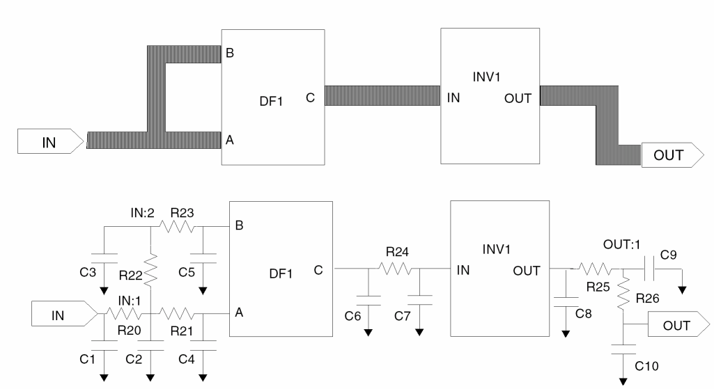
In this example, nonnative SPICE statements start with the notation “*|” to differentiate them from native SPICE statements.
.SUBCKT BUFFER OUT IN
*
* Net Section
*
*|GROUND_NET VSS
*
*|NET IN 1.221451PF
*|P (IN I 0.0 0 10)
*|I (DF1:A DF1 A I 0.0 10.0 10.0)
*|I (DF1:B DF1 B I 0.0 10.0 20.0)
*|S (IN:1 5.0 10.0)
*|S (IN:2 5.0 20.0)
C1 IN VSS 1.17763E-01PF
C2 IN:1 VSS 2.76325E-01PF
C3 IN:2 VSS 2.86325E-01PF
C4 DF1:A VSS 2.70519E-01PF
C5 DF1:B VSS 2.70519E-01PF
R20 IN IN:1 1.70333E00
R21 IN:1 DF1:A 1.29167E-01
R22 IN:1 IN:2 1.29167E-01
R23 IN:2 DF1:B 1.70333E00
*
*|NET BF 2.87069E-01PF
*|I (DF1:C DF1 C O 0.0 10.0 10.0)
*|I (INV1:IN INV1 IN I 0.0 30.0 20.0)
C6 DF1:C VSS 2.08719E-01PF
C7 INV1:IN VSS 7.83500E-02PF
R24 DF1:C INV1:IN 1.80833E-01
*
*|NET OUT 1.48478E-01PF
*|S (OUT:1 45.0 10.0)
*|P (OUT O 0.0 50.0 5.0)
*|I (INV1:OUT INV1 OUT O 0.0 40.0 20.0)
C8 INV1:OUT VSS 1.47069E-01PF
C9 OUT:1 VSS 6.32813E-03PF
C10 OUT VSS 7.76250E-03PF
R25 INV1:OUT OUT:1 3.11000E00
R26 OUT:1 OUT 3.03333E00
*
* Instance Section
*
XDF1 DF1:A DF1:B DF1:C DFF
XINV1 INV1:IN INV1:OUT INV
.ENDS
Non-native SPICE syntax and conventions are described below.
NET indicates the beginning of a new net description.
netName assigns each net statement a unique net name.
netCap specifies the total capacitance associated with the net. netCap includes capacitances to ground and capacitances to nearby wires. It includes a numerical value (which can sometimes be zero) and a unit name, usually PF, with no space between. Because the NET statement includes the total capacitance, you can examine the NET statement to extract the sim.cap format from the DSPF format.
Pins, instance pins, subnodes, and all the R/C descriptions that characterize the net follow the NET statement.
P {(pinName pinType pinCap [xCoord yCoord])}
P denotes pins in the net. Each pin description is delimited by parentheses and contains the information for its name (pinName), its type (pinType), its generalized capacitance value (pinCap), and its x coordinate location (xCoord) and its y coordinate location (yCoord). Multiple pin descriptions can be listed on one line.
pinType can be P (power), G (ground), C (clock), I (input), O (output), B (bidirectional), and X (unspecified).
pinCap consists of a capacitance value followed by any number of optional R/C pairs. For example
C0 [R1 C1 R2 C2 ...].
This format lets you model the pin characteristics by a higher order equivalent R/C ladder circuit than is represented by a single capacitor. The order of the equivalent circuit is increased from the first order (represented by C0) by attaching R/C pairs. The value of each capacitance is determined by a numerical value and a unit specifier such as PF. Use the generalized pin capacitance only if the pin type is I, O, or B. With other pin types, pinCap is dropped. In this case, you should use a number (for example, 0) as a place holder.
xCoord and yCoord describe a pin location (optional).
I {(instPinName instName pinName pinType pinCap [xCoord yCoord]..)}
I describes instance pins in the net. Each instance pin description is delimited by parentheses. The pinName, pinType, pinCap, and xCoord and yCoord follow the same format as described in the P statement. The description of the instance pin location is optional. Multiple instance pin descriptions can be listed on one line. The xCoord and yCoord can be repeated for feedthrough pins.
instPinName is the instance pin name component obtained by concatenating the instName and the pinName with a delimiting character specified by the DELIMITER statement.
instName is the instance name component.
pinName is the name of the pin in the master of the instance.
S {(subnodeName [xCoord yCoord])}
S denotes subnodes in the net. Each subnode description is delimited by parentheses and contains the name of the subnode and its location. A subnode name is obtained by concatenating the net name and a subnode number by a colon (netname:1). Multiple subnode descriptions can be listed in one line.
GROUND_NET specifies the ground net for loading capacitors. It must precede the NET statement.
netName is the name of the ground net.
This statement specifies the character C as the delimiter used to construct the instance pin name instPinName. If you do not include this statement, the default delimiter character, colon (:), is used.
For native SPICE statements, a continuation line begins with a plus sign (+) in the first column. For other statements, a continuation line begins with an asterisk and a plus sign (*+) in the first and second columns. The maximum number of continuation lines allowed is 1000.
RSPF Format
The DSPF file contains complete circuit information extracted by a parasitic extractor. Although this information is indispensable for debugging purposes, this can be too much data to use for circuit simulation or timing simulation.
One of the major applications of the parasitic circuit extractor is analysis of interconnect nets created by automatic placement and routing tools. In such applications, you do not usually require comprehensive circuit simulation of the parasitics; however, you might be very concerned about the total delays introduced by interconnect because the interconnect delays tend to limit the overall system performance. Traditionally, a delay calculator is invoked to perform the delay analysis. Arbitrary interconnect structures have to be reduced to a simpler form to allow fast delay calculation. The most common simplification is to reduce an interconnect net to a total capacitance, ignoring the effects of resistance and net topology.
The RSPF format is very similar to DSPF format except for the syntax in the spf_type and net_block sections. In addition to the keywords defined in the DSPF file, two extra keywords are used in the RSPF format: the DRIVER and the LOAD statements. The purpose of these two statements is to identify the driver-load relationship. The following syntax description shows only the syntax specific to RSPF.
qstring represents the version number of the SPF format.
NET netName driver_def {subNode_def} resistor_def2 capacitor_def2 {load_def {subNode_def} voltage_def resistor_def?}
NET indicates the beginning of a new net description.
driver_block describes the driver pin of the net followed by an optional subNode, then two resistors and two capacitors to form the driver block.
subNode_def is the same as that in DSPF format except that it does not output a subnode’s coordinates.
load_block describes the load pin of the net followed by an optional subNode, then a voltage-controlled voltage source, resistor, and capacitor to form the load block. The load block is optional because one pin nets are typically drivers with no load.
driver_def represents the driver pin of the net. It starts with the DRIVER keyword followed either by a top-level pin or an instance pin. For an instance pin, the instance pin name is obtained from the instance name and the pin name by concatenating them with a delimiter The default delimiter is a colon (:).
load_def represents the load pin of the net. It starts with the LOAD keyword followed either by a top-level pin or an instance pin.
voltage_def is a native SPICE statement.
RSPF Example
The following sample circuit is shown in RSPF format.
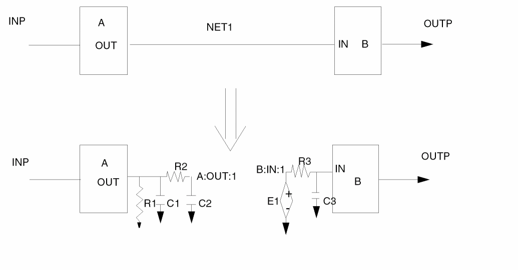
*|RSPF 1.0
*
*|DESIGN "ABC"
*|DATE  "September 8, 1995 20:10:00"
*|VENDOR "CADENCE"
*|PROGRAM "PREVIEW"
*|VERSION "PREVIEW_1.0"
*|DIVIDER /
*|DELIMITER :
*
.SUBCKT MODULE1 OUTP INP
*|GROUND_NET VSS
*
* Net Section
*|NET INP 1.7534PF
.
.
.*
*|NET NET1 0.8405578PF
*|DRIVER A:OUT A OUT
*|S (A:OUT:1)
R1 A:OUT VSS 2.84626E02
R2 A:OUT A:OUT:1 6.23854E02
C1 A:OUT VSS 0.533474PF
C2 A:OUT:1 VSS 0.392564PF
*|LOAD B:IN B IN
*|S (B:IN:1)
E1 B:IN:1 VSS A:OUT VSS 1.0
R3 B:IN:1 B:IN 1.4835E03
C3 B:IN VSS 1.0PF
*
*|NET OUTP 0.83975PF
...
.
*
*Instance Section
*
XA ...
XB ...
.
.ENDS
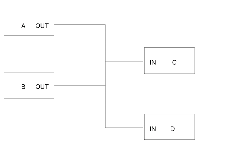
RSPF Example with Multiple Drivers and Multiple Loads
For a general multiple-driver and multiple-load net, a separate equivalent reduced model must be created for each driver-load pair.
*|RSPF "1.0"
*
*|DESIGN "ABC"
*|DATE  "December 8, 1995 20:10:00"
*|VENDOR "CADENCE"
*|PROGRAM "PREVIEW"
*|VERSION "PREVIEW_1.0"
*|DIVIDER "/"
*|DELIMITER ":"
*


.SUBCKT MODULE2 OUTP INP
*|GROUND_NET VSS
*
*Net Section
*
.
.
.
*|NET net 5.4982PF
* 1st driver pin group

*|DRIVER A:OUT A OUT
*|S (A:OUT:1)
R1 ...
R2 ...
C1 ...
C2 ...
*|LOAD C:IN C IN
*|S (C:IN:1)
E1 ...
R3 ...
C3 ...
*|LOAD D:IN D IN
*|S (D:IN:1)
E2 ...
R4 ...
C4 ...
* 2nd driver pin group
*|DRIVER B:OUT B OUT
*|S (B:OUT:1)
R5 ...
R6 ...
C5 ...
C6 ...
*|LOAD C:IN C IN
*|S (C:IN:1)
E3 ...
R7 ...
C7 ...
*|LOAD D:IN D IN
*|S (D:IN:1)
E4 ...
R8 ...
C8 ...
*
*|NET next_net 1.9387PF
.
.
.
*
*Instance Section
*
.
.
.
XA ...
XB ...
XC ...
XD ....
.
.
.ENDS
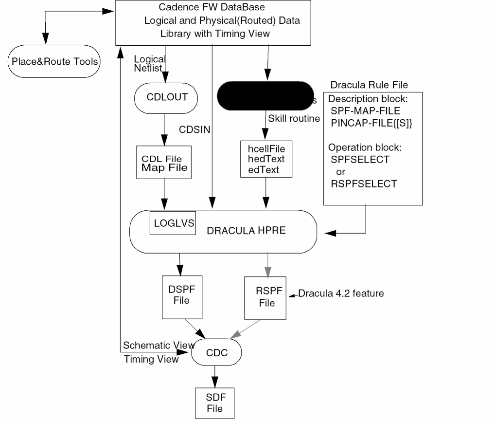
Dracula, CDC, DSPF and RSPF Flow
The following example illustrates the flow between Dracula, CDC, DSPF, and RSPF.
Return to top