8
Using Parametric Data (LPEPRO)
LPEPRO has been retired, and will be no longer supported as of December 31, 2008. Use the DRAC2CDL executable in order to generate a CDL netlist from specific Dracula binary files. To learn more about DRAC2CDL refer to Chapter 10, “Using DRAC2CDL Netlist Generator,”.Chapter 8 discusses the following for LPEPRO in Dracula:
- LPEPRO Overview
- Terminal Commands
- Administrative Commands
- Network and Gate Commands
- Delay Value Command
- Path Analysis Commands
- Report Commands
- Scanning Layout Parameters
- SPICE Generator
- Logic Gate Generator
- Calculating Delay
LPEPRO Overview
Even on a small chip, a large amount of parametric data is extracted from the layout and the information you need is hidden in it. The Layout Parameter Extraction Postprocessor (LPEPRO) is an interactive program that lets you
- View parametric information
- Generate logic network information from a layout
- Produce SPICE files for selected paths
- Verify the timing of selected paths based on layout parameters
You use LPEPRO after executing Layout Parameter Extraction (LPE). An LPE run with input schematics provides schematic data so you can annotate node names. LPE creates the parameter database and LPEPRO (the postprocessor) reads and interprets this database. For an explanation of the parameters extracted from a layout, refer to “LPE Overview”.
LPEPRO has the following features:
Using LPEPRO
To use LPEPRO, the LPE LPEDIR.TAB file, the LPE PARSET.TAB file, and the optional LVSLOGIC.DAT schematic file must be present in the directory in which you ran the LPE job. If you use a logic level schematic netlist to run LPE, you need to issue a SAVE LOGIC command before the CONVERT command when you run LOGLVS. (For a CDL, SPICE, or SIMON netlist, you don’t need to issue a SAVE LOGIC command).
If you provide schematic data, LPEPRO uses the node names. If you provide only layout data, the program uses the names in the layout whenever possible; otherwise, it assigns internal node numbers. You can choose whether to use schematic data with the GET LAYOUT, GET SCHEMATIC, or GET SPICE commands.
With the layout parameter scanner, you interactively select the information you want by specifying the range of a value, by specifying a window on the layout, or by providing node names.
If you do not have schematic logic data, LPEPRO generates basic gates from the layout database. The program recognizes NANDs, NORs, inverters, and several composite gates. If LPEPRO does not recognize the circuit, it generates parallel or serial devices whenever possible or leaves the transistors as is. You can then use this netlist in simulation or update it for a future LVS run.
The SPICE generator creates a SPICE file of a small cell, of selected paths, or of the whole chip. You select paths by specifying the starting and ending points. The SPICE file includes all elements along the specified paths. You can select capacitance by its value, and you can do a detailed timing analysis using a circuit simulator.
Selected path timing analysis provides logic schematic data for verifying the timing of the logic network, not the memory cell. LPEPRO calculates the delay of each cell on layout parameters W, L, and C, using the arithmetic equation in the “Extracting Electrical Parameters” chapter. After it identifies the selected paths, you can generate the SPICE file to do detailed timing analysis.
You can direct reports to a terminal, printer, or specified file.
Terminal Commands
You can interactively start all commands in LPEPRO. For some systems, you can group these commands in a file and use a system job control language to submit them as a batch job. LPEPRO commands can be classified into the following categories:
-
Administrative commands
Specifies a file name for the STORE command (The default file name is IMAGE.LIS.)
-
Commands to read in the network and generate logic gates
Retrieves network information from a schematic database or layout database
-
Command to get delay values
-
Commands for path analysis
-
Commands to generate reports (parameter scanning, SPICE or logic netlist, delay values, path outputs, and so forth)
All terminal commands are case-insensitive and you can abbreviate them to their first three letters.
LPEPRO generates a journal file and also lets you input a rules file. The JOURNAL.LPE file contains a list of every command you entered during the session. To use this file in your next LPEPRO session, rename the journal file (for example, from JOURNAL.LPE to session1.del) so that LPEPRO does not overwrite it.
Administrative Commands
This section describes in detail the administrative commands for LPEPRO.
DISK
DISK filename
Description
Specifies a file name for the STORE command.
Arguments
The name for the file. The default file name for the STORE command is IMAGE.LIS.
Example
In this example, the DISK command closes the current file and opens a file with a new name.
DISK PARAM.DAT
INPUT
INPUT filename
Description
Reads in commands from a file.
Arguments
The name of the file containing the commands. The file name is limited to 32 characters.
You cannot specify journal.lpe because it is being written to during the LPEPRO session.
RESET
RESET ALL
 [START]
 [END]
 [MASK]
 [DELAY]
 [PATH]
Description
Resets network and parameter information, such as starting points, ending points, masked nodes, delays, and path information.
Arguments
Resets all program information and begins the LPEPRO program from the beginning.
Resets masked nodes, either user-specified nodes or nodes found with the MASK .FEEDBACK command.
Resets all delay values to zero.
Resets the path information file and the starting and ending points in the PATH command.
Example
RESET PATH
RESET ALL
SAVE
SAVE DATA
Description
Saves the current network information onto the disk.
Arguments
Saves the current network or timing information on disk in the network.sav file. You cannot change this file name.
EXIT
EXIT
X
Description
Network and Gate Commands
This section describes in detail the network and gate commands for LPEPRO.
GET
GET SCHEMATIC
 LAYOUT  field_1
 SPICE
 DATA
Description
Retrieves network information from layout, schematic, or previously saved data.
Note: Do not run LPEPRO on a job that uses the LPECHK[X] command because the input of netlist information requires that reductions of transistors to PUP, SDW, and so on be performed. The GET command generates unusable data if LPECHK[X] outputs are used for LPEPRO.
Arguments
Recovers network information that you saved with the LOGLVS SAVE LOG command. If you did not save the log file in LOGLVS, use the GET SPICE command to recover the network information. If the input schematic is SPICE or CDL only, use the GET SPICE command.
Reconstructs a logic network from the transistor level netlist extracted from the layout database. If field_1 is equal to SCHEMATIC, use the transistor level netlist generated by LOGLVS from SPICE input.
Has the value of SCHEMATIC. Can only be used with the GET LAYOUT command. The GET LAYOUT SCHEMATIC command reconstructs the logic network from the SPICE data input. You can also use GET SPICE.
Reconstructs the logic network from the SPICE data input. Same as GET LAYOUT SCHEMATIC.
Recovers saved network information whether the data was saved with the LOGLVS SAVE LOG command or the LPEPRO DAVE DATA command.
Examples
GET SCH
GET LAY SCH
GET DAT
GET SPICE
DELAY
DELAY .DEFAULT=R1/F1[output/input=R1/F1] [ output=R2/F2]
Description
Assigns a default rise and fall delay value to all output nodes. Also lets you assign a delay value to an output node.
Arguments
Updates all output nodes with delay values equal to zero. You must use the equal sign (=) to indicate that a delay specification follows.
Indicates rise and fall delay time specification. The delay value must be an integer. If you specify the rise value only, the slash (/) can be omitted. The value after the slash (/) is interpreted as the fall delay.
Updates the delay of one output node of wired-ORed connections. Output is the output node of several gates (wire-OR). Only the delay of the gate with the input node input is updated.
Updates the delay of the specified output node. Delays of all gates with this node for output are updated.
Examples
DELAY .DEFAULT=200/250
DELAY OUTPUT1=10/20,OUT2/IN1=10/20
Delay Value Command
This section describes in detail the delay value command for LPEPRO.
CALCULATE
CALCULATE  PARAMETER = arithmetic equation
       DELAY/option
Description
Specifies the formula to use in the delay calculation or parameter calculation. You can specify more than one option in this command.
Arguments
Specifies the equation for the parameter calculation. The drain and source node of each transistor are checked separately.
The formula you specified in the delay or parameter calculation. LPEPRO recognizes the following parameters:
The operations you can specify include the following:
Calculates the delay according to the formula in the delay calculation. Length and width cannot be used separately; only the ratio of these two values can be used in the equation. The /option value is the optional delay type specification. It can have the following formats:
Examples
You can include a real number, or a number in scientific notation, in the equation.
CALCULATE DELAY = (L/W)*C
CAL PARA = 30*(L/W)
CAL DELAY/ON/OFF = 25*(L/W+0.5)*C
CAL DELAY/GATE = BINV,DINV=10*(L/W+10)*C
In a parameter calculation, capacitance units are in pf. In a delay calculation, capacitance unit is ff or whatever value (capacitance per unit area) you specified in the PARASITIC CAP command.
Delay calculations always result in an integer value.
Path Analysis Commands
This section describes in detail the path analysis commands for LPEPRO.
LPATH
LPATH
Description
Performs the longest path analysis. If there are feedback loops, you must mark them with the MASK .FEEDBACK command.
The longest path is defined as a path from any input that has the longest delay value in the network. If there are nodes that cannot be reached because of feedback or other reasons, they are not included.
To cut feedback loops, use the MASK .FEEDBACK command. The LPEPRO program might not be able to cut the feedback loops at the proper places. Review the masks with the TYPE .MASK command after the feedback loops are cut.
To perform path analysis, provide the starting nodes. The starting nodes can be pad type nodes, nodes defined in the schematic as input, or nodes defined by the START command.
To perform path analysis with a schematic netlist that does not come from SPICE or CDL input, you must first issue a SAVE LOG command in LOGLVS. In LOGLVS, you must issue SAVE LOG before the CONVERT command.
SPATH
SPATH
Description
Performs an analysis of the shortest paths.
The shortest path is defined as a path from any input that has the shortest delay value in the network. If nodes cannot be reached because of feedback or other reasons, they are not included.
To cut feedback loops, use the MASK .FEEDBACK command. The program might not be able to cut the feedback loops in the proper places. Review the masks with the TYPE .MASK command after the feedback loops are cut.
To perform path analysis, provide the starting nodes. The starting nodes can be pad type I nodes defined in the schematic as input or nodes defined by the START command.
To perform path analysis with a schematic netlist that does not come from SPICE or CDL input, you must first issue a SAVE LOG command in LOGLVS. In LOGLVS, you must issue SAVE LOG before the CONVERT command.
PATH
PATH
Description
Finds all elements between your specified starting and ending points. You can then print the SPICE file.
An element is included in the path if it appears in both the forward and backward tracing program. Feedback loops result in more elements being included in the path. To avoid this, use the MASK .FEEDBACK command to mask out feedback loops.
To exclude a branch, use the MASK NODE-NAME command. To select a new path, use the RESET PATH command, then redefine the starting and ending nodes before issuing another PATH command.
If the schematic netlist does not come from SPICE or CDL input, a SAVE LOG must be done in LOGLVS or no path analysis can be done with the GET SCHEMATIC command. When running LOGLVS, you must issue SAVE LOG before the CONVERT command.
START
START node1,node2,...noden
Description
Specifies starting points in the PATH, LPATH, and SPATH commands.
Arguments
The names of the nodes. If the network is from the schematic, use the names in the schematic. If the network is from the layout, use the node name or the node number.
Example
STA A1,A2,A3
END
END node1, node2,...noden
Description
Specifies ending points in the PATH, LPATH, and SPATH commands.
Arguments
The names of the nodes. If the network is from the schematic, use the names in the schematic. If the network comes from the layout, use the node name or the node number.
MASK
MASK .FEEDBACKarg1...argn(orname01/nameI1,nameI:name02,) ....nameOn/nameIn
Description
Masks out paths. Use this command to mask out feedback loops that prevent the program from finding critical paths.
Arguments
Masks out all feedback loops. Initializes the network to find feedback loops. If there are nodes that cannot be initialized, displays the name of the node.
Specifies one or more of the following forms:
Examples
MASK .FEEDBACK
MASK A1, B1, OUT1/A2
UNMASK
UNMASK arg1...argn
Description
Selectively removes a masked node. Use this command to unmask nodes that are currently masked. For example, you can use this command to unmask nodes masked with the MASK .FEEDBACK command.
Arguments
Specify one or more of the following forms:
|
The name of the WOR output name. Read as gate name 01; one of its input pins is named I1. |
|
|
The name of the input. Read as the I2 input pin name of O2 device name. |
|
Example
UNMASK S1,B1,I1:02
Report Commands
This section describes in detail the report commands for LPEPRO.
PRINT, TYPE, and STORE
PRINT field 1, field 2, field 3
TYPE
STORE
Description
Directs your output to the device you choose. PRINT directs output to a printer. TYPE directs output to your screen, and STORE directs output to a file.
Field 1 is the subcommand of PRINT, TYPE, or STORE. Field 2 can be a subcommand of field 1 if it begins with a period (.). You can use any of the following subcommands and their arguments with the TYPE/PRINT/STORE commands.
SPICE Subcommand Arguments
PRINT/TYPE/STORE the path in SPICE format.
Specifies the threshold value of the capacitance in pf over which the capacitance is output.
Indicates that schematic names are to be used. If no schematic is available, use layout text. To recover the SPICE node number, use the /SCH option.
Outputs the shortest path in SPICE format. Use the SPATH subcommand only after the shortest path timing analysis is performed.
Outputs the longest path in SPICE format. Use the LPATH subcommand only after the longest path timing analysis is performed.
This field can only be used with the LPATH or SPATH subcommands. :n1,...nn are the nth path specifications. Prints n1th, ...nnth longest or shortest paths.
The names of the nodes. Can only be used with the LPATH or SPATH subcommands. Indicates that elements along the longest or shortest paths to node 1,...node n are included in the SPICE file.
Outputs the path in SPICE format.
Outputs all network information including parasitics and LDD devices in SPICE format. This command is usually reserved to generate the SPICE file of a cell.
SPICE Examples
PRINT SPICE PATH
STORE SPICE/SCH/CAP=0.01PF LPATH=1
TYPE SPICE SPATH Q1, QBAR1
PATH, LPATH, and SPATH Subcommand Arguments
Prints all elements along the longest or shortest paths.
Outputs the first n longest or shortest paths.
Prints paths with a delay greater than or equal to m.
Prints paths with a delay less than or equal to 1.
The longest or shortest path to the listed nodes.
LPATH Examples
PRINT LPATH 20
STORE LPATH Q1, QBAR1, Q, QBAR
DELAY Subcommand Arguments
The ratios of fall/rise delay, respectively.
Prints a gate or output node with delay greater than or equal to n.
Prints a gate or output node with delay less than or equal to m.
Prints the delay value of the gates specified.
DELAY Examples
PRINT DELAY A1,A2
TYPE DELAY/R/F 1
CAPACITANCE Subcommand Arguments
Prints the detailed cross-couple capacitance; otherwise, the lumped capacitance is printed.
Optional type specification; when T is absent, all types are printed. You can specify more than one capacitor type.
Prints nodes with capacitance value greater than or equal to R1. This value is a real number and pf is the unit. When a unit is absent, pf is assumed. You can use > or .GE for “greater than or equal to.”
Prints nodes with a capacitance less than or equal to R2. This value is a real number in pf units. When a unit is absent, pf is assumed. You can use < or .LE for “less than or equal to.”
Prints nodes with a capacitance range of V1 and V2. The values V1 and V2 are real numbers in the pf unit.
CAPACITANCE Example
TYPE CAP[N,P,X] >0.1
MOS Subcommand Arguments
Prints transistor information including areas and perimeters.
Optional type specification. When T is absent, all types are printed.
Indicates that only the transistor width is checked.
Indicates that only length is checked. When both are missing, both width and length are checked.
Indicates that the ratio of width to length is checked.
Indicates that the ratio of length to width is checked. The specification can only be used with R1 and R2 and .RANGE =V1,V2.
Prints transistors whose length or width is greater than or equal to R1; or whose width/length or length/width ratio is greater than or equal to R1. You can use > or .GE for “greater than or equal to.”
Prints transistors whose length or width is less than or equal to R2, or whose length/width, width/length ratio is less than or equal to R2. You can use < or .LE for “less than or equal to.”
Prints information about transistors connected to these nodes.
W/L information of transistors inside the (X1,Y1)/(X2,Y2) window specified by X1,Y1 and X2,Y2 are printed. Parentheses are optional, the slash (/) is required. X1, Y1, X2, and Y2 use a natural unit.
W/L information of transistors n1,...nn are printed; n1,...nn are internal device numbers used in the program.
Prints a node with W/L information in the range V1,V2. The values V1, V2 have the same units as R1 and R2.
MOS Examples
TYPE MOS[D]/W >0
PRINT MOS .WIND = 100,100/-100,-100
DIODE Subcommand Arguments
Value of A1, A2, A3 or P1, P2, P3. Use this option with R1, R2, or .RAN=V1,V2.
Prints diode information if the parameter is greater than or equal to R1. You can use > or .GE for “greater than or equal to.”
Prints diode information if the parameter specified by /option is less than R2. You can use < or .LE for “less than or equal to.”
Prints diode information from the specified nodes.
Window specification. Prints diode information for diodes inside window (X1,Y1)/(X2,Y2). Parentheses are optional. Slash (/) is required. X1,Y1 and X2,Y2 use a natural unit.
Outputs diode information with the given device numbers.
Prints nodes with parameters in the range of V1 and V2.
DIODE Examples
TYPE DIO[D] A1,B2,IN1
PRINT DIO[D] .WINDOW=(100,200)/(230,300)
PARAMETER Subcommand Arguments
Checks the parameter calculated by the CALC command.
Prints the ratio parameter value. /U and /D represent the pull-up parameter value and the pulldown parameter value, respectively. /U/D represents the ratio of the pull-up parameter value to the pulldown parameter value and /D/U is the reverse.
Prints nodes whose parameters, calculated by the CALC command, are greater than or equal to R1. You can use > or .GE for “greater than or equal to.”
Prints nodes whose parameters are greater than or equal to R2. You can use < or .LE for “less than or equal to.”
Prints parameters of the specified nodes.
Window specification. Direct the program to bring (X1,Y1)/(X2,Y2) the parameter information with this window. Parentheses are optional, slash (/) is required. X1,Y1 and X2,Y2 use a natural unit.
Outputs parameter information of MOS n1,n2,...nn.
Prints the node whose parameter is within the range V1 and V2. V1 and V2 are real numbers.
PARAMETER Examples
TYPE PARAM >21
PRINT PARAM .WIND = 100,100/-100,-100
PRINT and TYPE are recognized only after you have specified the parameter equation.
MASK Subcommand
Prints the names of masked nodes or pins.
START Subcommand
Displays all specified starting nodes.
END Subcommand
Displays all specified ending points.
PATH Subcommand
Prints all elements between your specified starting and ending points.
UNREACH Subcommand
Prints any element that cannot be reached by input signals.
Scanning Layout Parameters
LPEPRO lets you review MOS, DIODE, CAPACITANCE, or user-defined parameters. The commands you use to review parameters start with PRINT, TYPE, or STORE.
The DISK command changes the file name in the STORE command. After you issue a PRINT, TYPE, or STORE command, the following become subcommands:
MOS DIODE CAPACITANCE PARAMETER RES LDD
To review the above subcommands, use one of the following values:
You can also select the parameters using node names or node numbers. For parameters that involve the location of MOS, DIODE, or PARAMETER elements, use the .WINDOW command to select a window.
Identifying Nodes in the Layout
The LPEPRO program uses names, if available, to report results. If names are not available, the scanner uses an internal node number. There are two ways you can specify node names in the layout database:
If you specify the GET SCHEMATIC command, LPEPRO uses elements or nodes on the schematic data, including node names. Without the GET SCHEMATIC command, LPEPRO assumes that only layout data is provided. In this case, only those nodes with text have node names. LPEPRO assigns an internal node number to all of the other nodes.
The internal node numbers assigned by the LPEPRO program are difficult to identify. To solve this problem, do the following:
- To zoom into the relevant transistors so you can identify the node numbers, use the .WINDOW command. Based on the known numbers, you can identify the internal node numbers.
- To display the network connection, use the TYPE MOS command. After the relationship of the connection is established, you can trace a node number.
- Plot the relevant nodes.
- Label the significant nodes.
- Provide the schematic data.
MOS Subcommand
The MOS subcommand lets you check transistors for width, length, width/length ratio and length/width ratio. You select these values by specifying their value range. LPEPRO assumes that width and length are in natural units and ignores the unit you specified in the command. To zoom into an area, use the .WINDOW command.
Example 1
:TYPE MOS[D]/W .LT 4
Checks any transistor with a width of less than 4.
Arguments
Specifies that only D-type MOS are checked.
Specifies that width is checked. There can be no blank spaces between the bracket (]) and the slash (/).
Example 2
:PRI MOS[E]/L/W .GE 10
Checks any transistor with an L/W ratio greater than or equal to 10.
Arguments
Indicates that the length/width ratio is checked. No blank spaces are permitted between slashes (/).
Example 3
:TYPE MOS/W/L .RANG=10,20
Checks any transistors whose W/L ratio are between 10 and 20.
Example 4
:TYPE MOS .WIND=100,200/200,100
Finds the transistors in the X1=100, Y1=200, X2=200, Y2 =100 window. .WIND is the keyword of the WINDOW command. X1, Y1 and X2, Y2 immediately follow the equal sign (=). A slash (/) is required to separate the two coordinates.
Example 5
:TYPE MOS A1,B10,20
Finds all transistors connected to A1, B10, 20 nodes, where A1 and B10 are either schematic names or names put in the layout database. In this example, A1 is not interpreted as a keyword because it does not have a period (.).
The outputs of all of these examples are similar. Each MOS is printed in the following format:
Mnumber Drain, Gate, Source, Substrate, Model,
L=length, W=width, X=x-coordinate, Y=y-coordinate
For W/L or L/W ratio, the ratio is printed before each MOS statement as a comment. For example,
* = 3.86
M10 GND, 9, 8, GND, NCHNL, L=0.35, W=2.00
X=-2.99, Y=-25.99
The node name is used when it is available.
CAPACITANCE Subcommand
The CAPACITANCE subcommand lets you review nodal capacitance. If the range of the capacitance value is specified, use the T option to select the capacitance type. Specify more than one type of capacitance inside brackets ([]). For example, CAP[N,P,X,Y] directs LPEPRO to select N, P, X, or Y types of capacitors only. LPEPRO sums up all capacitances without the T option or selected capacitances with the T option. To obtain detailed cross-couple information, use the /DETAIL option.
Example 1
:TYPE CAP .GT 1
Displays nodes with capacitances exceeding 1 pf.
Example 2
:PRINT CAP[N,P] .RANG=1,3
Prints node names with capacitances between 1 pf and 3 pf of N and P types.
Example 3
:STOR/DET CAP A1, B1
Detailed information of the nodal capacitance of A1, B1 nodes is stored on disk. The output has the following format:
A1/node1=npf :N    A1/node2 = mpf :X
A1/node3=upf :P    A1/node4 = lpf :Y
***TOTAL CAPACITANCE = R pf***
In addition to the total capacitance R pf, the capacitance between A1 and node1, A1 and node2,... and their corresponding capacitance type are displayed. If no /DETAIL option is specified, only the total capacitance for A1 and B1 nodes is stored.
DIODE Subcommand
The DIODE subcommand lets you to review diode information. The options for this subcommand are similar to those for the MOS command. Instead of width and length, there are six parameters: A1, P1, A2, P2, A3, P3. for more information about using this subcommand, refer to the ELEMENT MOS section in Chapter 13.
PARAMETER Subcommand
The PARAMETER subcommand lets you specify the arithmetic equation of W, L, and C parameters extracted from the layout. LPEPRO checks the parameter, calculates according to the equation provided, and displays those elements with parameters that fall within your specification. Specify the arithmetic equation with the CALULATE PARAMETER command, then use the TYPE PARAMETER command to review the result.
Arithmetic Equations
To specify the equation for the parameter, use the following command:
:CAL PAR = arithmetic equation
You can use the following symbols in the equation:
You can include a number, real number, or integer in the equation. For example
:CAL PARA = 100*(L/W)*C+10.2
In this case, the program takes the ratio of length to width, multiplies it by 100, multiplies it by the capacitance value, then adds 10.2.
LPEPRO assumes that width and length are in natural units and capacitance is in pf when it calculates the parameter. LPEPRO does not assign any unit to the result. You specify the equation and the interpretation. Once you provide the equation, you can review it as you would any other parameter.
Reviewing Parameters
To review parameters, use the PRINT, TYPE, or STORE PARAMETER command. These commands are similar to the MOS subcommand. All of the subcommands are the same, except for the /U, /D, /U/D, and /D/U options. For details about these options, refer to the Terminal Commands section in this chapter.
Example
:CAL PAR=(L/W)*C
:TYP PAR/U/D A1
This calculates and types the ratio of the pull-up parameter value to the pulldown parameter value for the A1 node. Parameter values are computed according to your formula.
:TYP PAR/U/D <3
This types all nodes whose pull-up to pulldown parameter ratio values are less than or equal to 3.
If you use the /U, /D, /U/D, or /D/U options, a PARASITIC CAP command must be specified so that every node in the circuit has a parasitic capacitor calculated for it. Otherwise, not all nodes are reported.
SPICE Generator
LPEPRO can generate a SPICE file for simulation purposes. The SPICE file can be the whole chip, a whole cell, or selected paths. You can specify a capacitance threshold value. The SPICE file includes only capacitances larger than the threshold value.
Whole Chip or Whole Cell
To generate a SPICE file for a whole circuit, use the TYPE command.
:TYPE SPICE/CAP=0.5 ALL
In the previous example, LPEPRO displays MOS information. The optional /CAP=0.5 specification displays only nodes with capacitances over 0.5 pf. Diode information follows the capacitance. There are two difficulties with this command:
- The command produces too much information and internal node numbers are used throughout the data.
- It is almost impossible to correspond these node numbers to node names in a schematic.
You can avoid generating too much information by not using this command for an entire chip. Use the TYPE SPICE ALL command to generate a SPICE file for a small cell, but do not use it for an entire chip.
If you provide schematic data, you can avoid the second problem by using the following commands:
:GET SCH
:TYPE SPICE/SCH/CAP=0.5 ALL
In this case, if you use the /SCHEMATIC option, node names from the schematic are used. These node names can be names used in your logic network data or in your original SPICE file. This SPICE file can be output as the reference for the simulation.
Use the DISK command to store the SPICE deck to a specified file name.
Selected Paths
If you use selected paths, you can select some elements from the chip and generate the SPICE file for them. Use one of the following methods:
- Elements between your specified starting and ending nodes
- Longest paths in the LPEPRO path analysis
- Shortest paths in the LPEPRO path analysis
For a description of longest/shortest path analysis, refer to the LPATH and SPATH commands in this chapter. The SPICE commands are as follows:
:TYPE SPICE/CAP=0.5 PATH or
:TYPE SPICE LPATH :3,5,10 or
:TYPE SPICE SPATH :10
You can use these commands whether you have schematic data, SPICE data, or no schematic data.
Schematic Data
For schematic data, prepare the file as follows:
-
To save the compiled logic network after LOGLVS compiles and before it converts the logic data in the transistor file, issue the following command:
:SAVE LOGIC
then enter:CONVERT
- To recover the schematic data, use the GET SCHEMATIC command. This command reads the compiled logic network that was saved when you executed LOGLVS.
- To mask out (or cut) the feedback loops, use the MASK .FEEDBACK command whenever necessary. LPEPRO identifies feedback loops and cuts them at the proper places. If after several iterations there are still nodes that cannot be initialized by an input signal, LPEPRO displays these nodes on your screen. Sometimes LPEPRO cuts the feedback loop in the wrong place.
- To review nodes that are masked by LPEPRO, use the TYPE.MASK command.
- To add new nodes, use the MASK command. To change masked nodes, use the UNMASK command.
-
To specify starting nodes and ending nodes, use the START and END commands. For example,
   :START A1, D1, A2,...
   :END B1, OUT1, OUT2
Where A1, D1, and A2 are the starting nodes and B1, OUT1, and OUT2 are ending nodes. These node names should be consistent with the names in your logic database. - To find the elements along the starting and ending nodes, use the PATH command.
- To review the result, use the TYPE PATH command. An element is included in the path if it appears on both the forward and backward tracing of the PATH command.
-
Display the SPICE file on your screen as follows:
:TYPE SPICE PATH
If this produces what you want, use the STORE command to store the results. (You can change the file name with the DISK command.) - To screen out unwanted capacitances, use the /CAP=valve option.
- To select another path or paths, use the RESET PATH command.
- Repeat steps 5 through 7 for another selection.
No Schematic Data
If there is no schematic data or if the schematic data is SPICE, proceed as follows:
-
To read the transistor level file and reconstruct the logic network from the layout, use the GET LAYOUT command.
For information on how LPEPRO handles this process, refer to the Logic Gate Generator section in this chapter. For SPICE data and original node names in SPICE, use the following command::GET LAYOUT SCH or GET SPICE
SCH indicates the data are from the schematic. LPEPRO reconstructs the network and recovers node names or numbers you used in the original SPICE deck. -
To cut the feedback loops, use the MASK .FEEDBACK command.
Because LPEPRO might not be able to form gates from some transistors, many discrete components might exist. LPEPRO might not be able to cut all feedback loops at the proper places. - To reselect the network loops to be cut, use the UNMASK and MASK commands.
- To select the elements you want to include in the SPICE output, follow steps 5 through 8 in the Schematic Data section of this chapter.
Logic Gate Generator
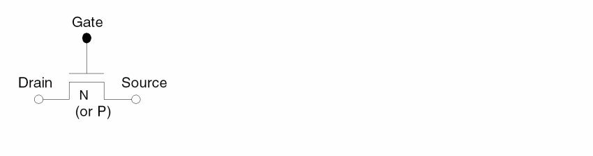
If you do not have schematic data or if your schematic data is in SPICE format, follow the instructions in this section. The logic gate generator recognizes only predefined primitive gates and handles only MOS technology. A primitive gate should have the following properties:
For unrecognizable networks, the program forms parallel pull-up, parallel pulldown, serial pull-up, or serial pulldown devices whenever possible, or it forms an N-type or P-type unidirectional transfer gate. As a last resort, the program uses an MOS device that has bidirectional properties. Once the logic network is reconstructed, selected paths can be formed. In most cases, selected path timing is done.
Using the Logic Gate Generator
You can generate a logic network from a SPICE file or from the layout.
When you generate the logic network from a SPICE file, every node has a number that the system treats as the node name. When the logic network is generated from the layout, only labeled nodes have names and Dracula assigns a number to unlabeled nodes. After the logic network is created, the naming conventions are as follows:
-
Program-assigned name: N-number is the internal node number. For example
N-301 Node 301
-
User-assigned name: The name in a SPICE file or I/O pad names. For example
   101  Node number 101 in SPICE data file.
   P1   Name used as label in the layout.
To generate the logic network from the layout, follow these steps:
-
Use the GET LAYOUT command, or if you want to create a logic gate from the SPICE file, use the GET LAYOUT SCHEMATIC command or the GET SPICE command.
Assuming that your SPICE file is the exact image of the layout, the difference between these two commands is that the logic network generated from a SPICE file has your user-assigned node names, while the network generated from layout has program-assigned node names (except for labels). - To create a network description file, use the STORE command.
- Change the file name in the STORE command with the DISK command.
- After the logic network is generated, select path and perform path timing analysis.
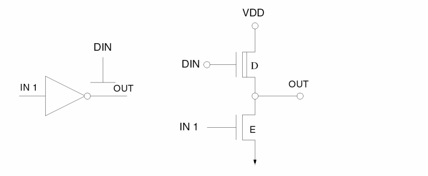
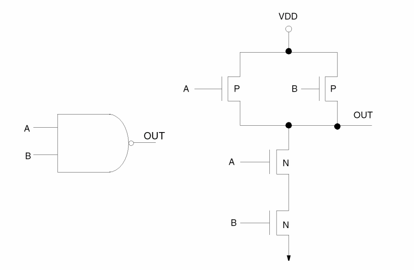
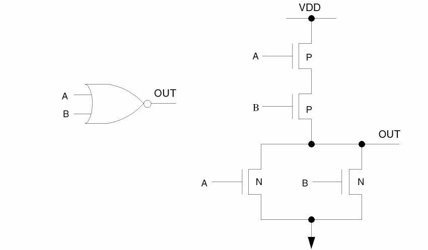
Gate Types
All gate types generated by the logic gate generator are listed below.
NMOS (or PMOS)
RES: Resistor
Used for NMOS only. A transistor is converted to a RES if
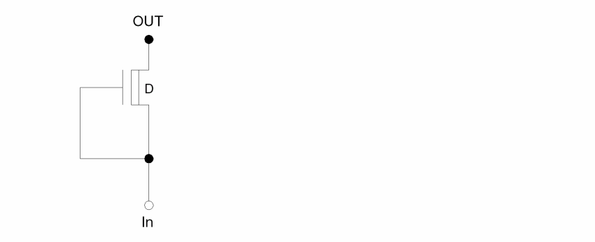
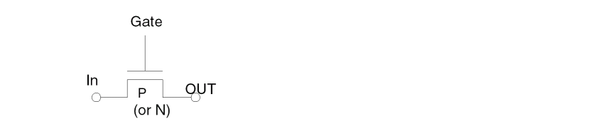
NXFR (or PXFR): N or P Type Transfer Gate
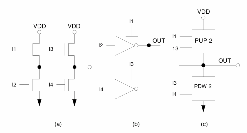
A MOS device is converted to NXFR (or PXFR) if the directionality of the MOS can be determined. Type N in a CMOS circuit or type E in an NMOS circuit is converted to NXFR. Type P in a CMOS circuit is converted to PXFR.
NRXF
Used for NMOS only. Resistive N-type transfer gate. A MOS is converted to NRXF if it is a non-E type in an NMOS circuit.

SUP: Serial Pull-Up Device
The cell name is SUPn where n is the number of a pull-up MOS gates.
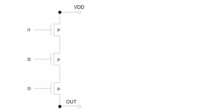
PUP: Parallel Pull-Up Device
The gate name is PUPn where n is the number of MOS gates.
SDW: Serial Pull-Down Device
PDW: Parallel Pull-Down Device
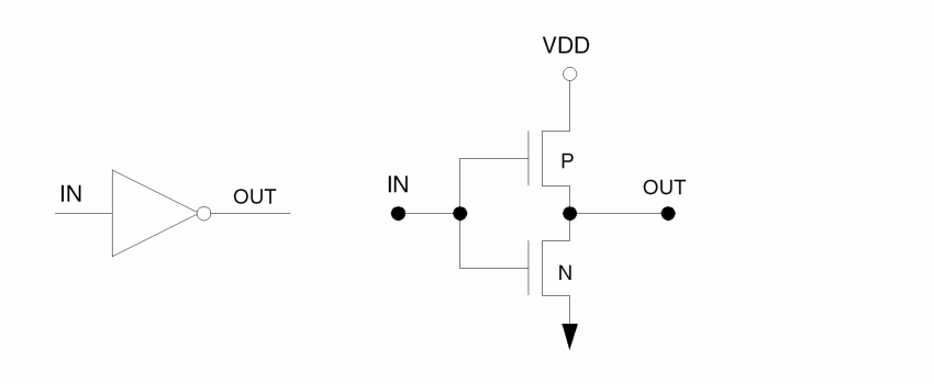
INV: Inverter
BINV: Buffer-Inverter
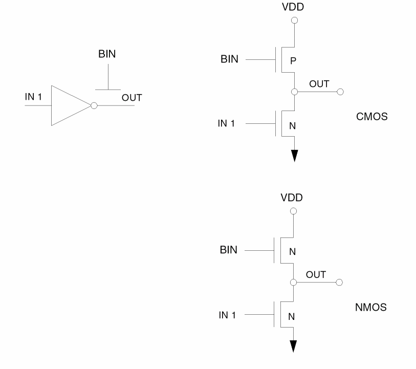
DINV: D-type Buffer-Inverter
NAND
For NMOS, only the depletion mode MOS, type D, is used to form the gate. Other types of pull-ups are not used.
NOR
AOI1: AND-OR Inverter Type 1
AOI2; AND-OR Inverter Type 2
AOI3; AND-OR Inverter Type 3
A0I4: AND-OR Inverter Type 4
AOI5: AND-OR Inverter Type 5
AOI6: AND-OR Inverter Type 6
OAI1: OR-AND Inverter Type 1
OAI2; OR-AND Inverter Type 2
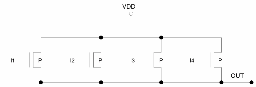
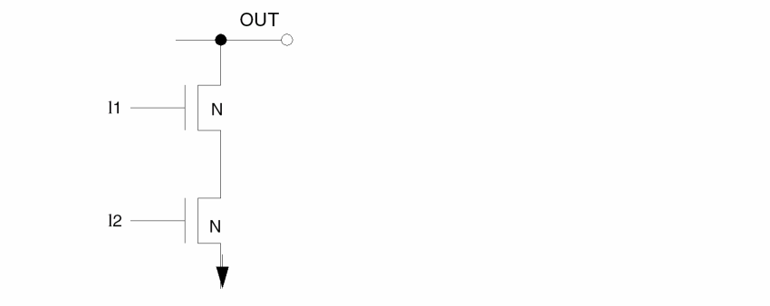
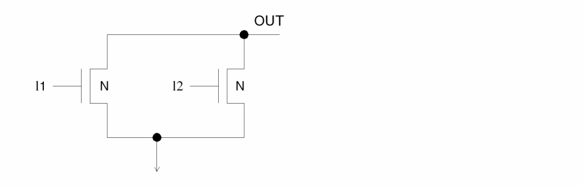
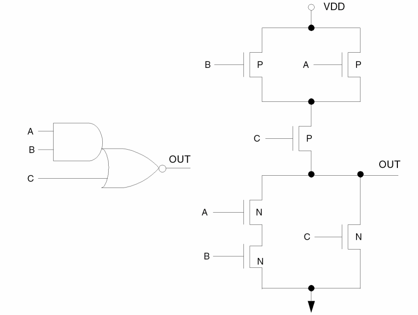
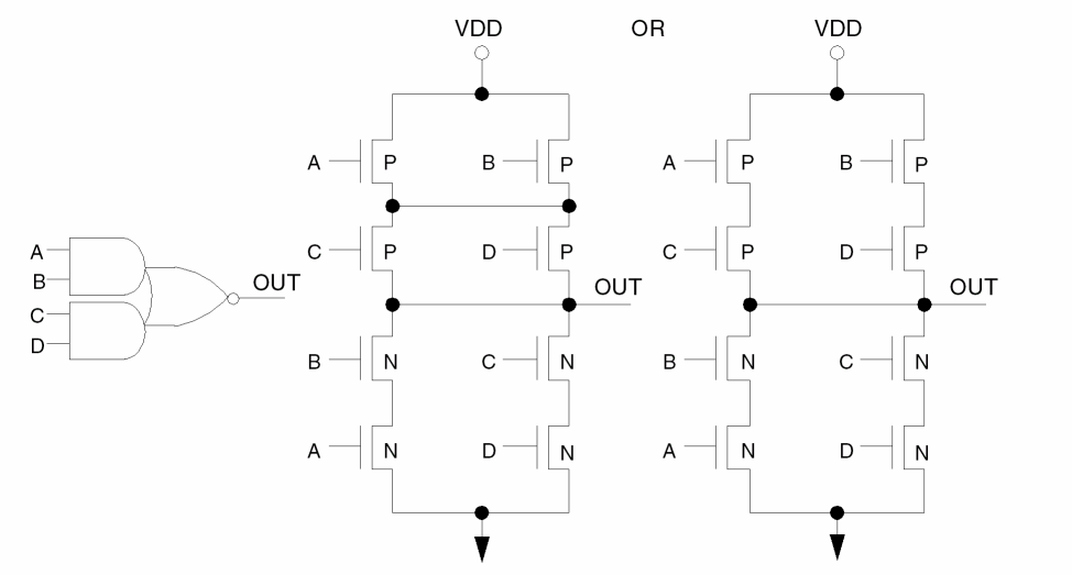
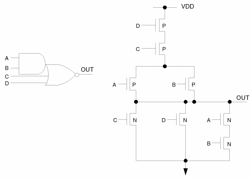
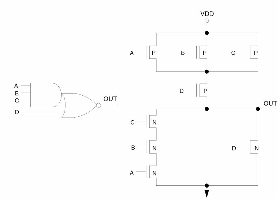
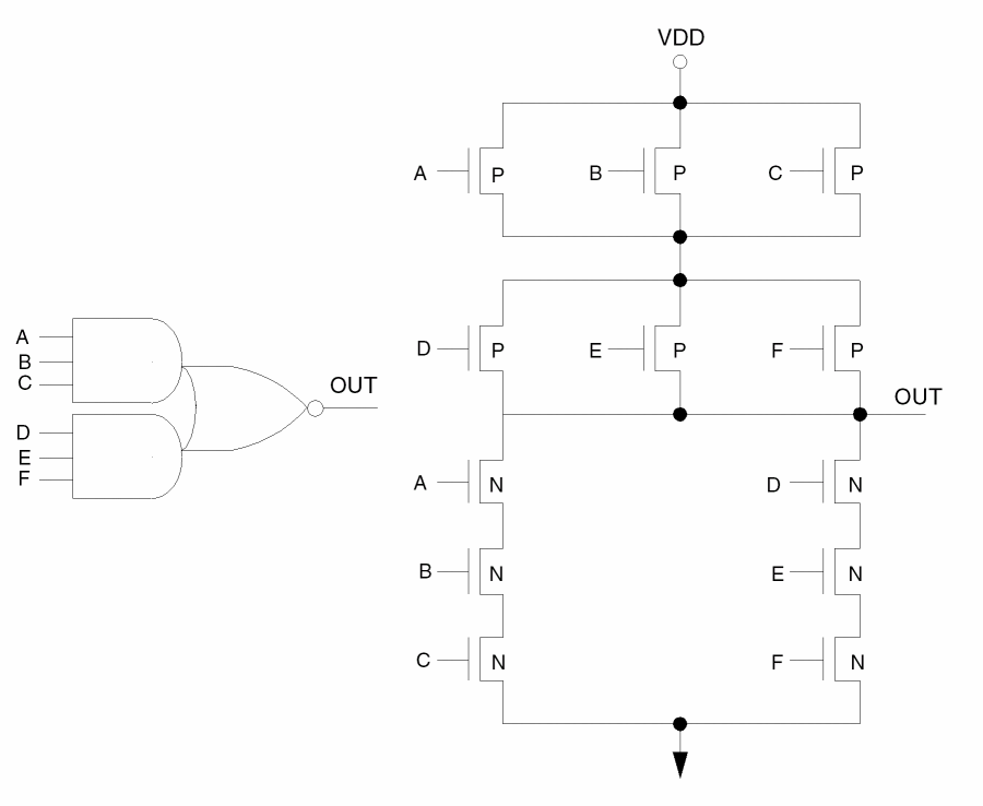
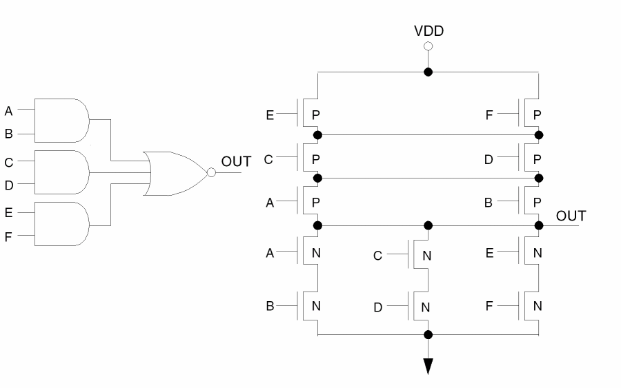
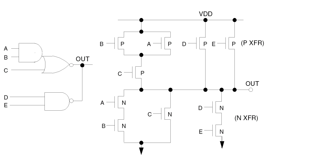
Wired-OR Examples
Wired-OR (or wired-AND) is defined as outputs of two or more connected gates. In the case of wired-ORs and wired-ANDs, the LPEPRO program does not recognize individual gates and creates a parallel up and parallel down structure. If the circuit is too complicated to form a parallel-up/parallel-down structure, transfer gates are used instead.
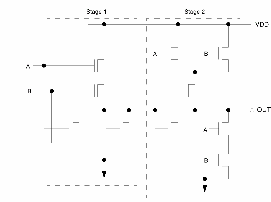
Two Buffer-Inverters Wired-OR
The circuit in (a) is converted to a two-input parallel pull-up and a two-input parallel pulldown (c) instead of two buffer-inverters as in (b).
AOI1 and NAND Gate Wired-OR
When a circuit is more complicated than a simple, parallel/serial structure, the program does not convert transistor circuits into gate equivalents and uses PXFR and NXFR instead.
Calculating Delay
An important function of length (L), width (W), and capacitance (C) of MOS transistor layout parameters is to calculate gate delay. Timing verification and logic simulation are calculated with the first order of delay information.
LPEPRO uses an arithmetic equation based on L/W and C in delay calculation. The effective L/W ratio is used for serial/parallel structures. Capacitance is defined as the total nodal capacitance (measured in picofarads - pf) of the output node of the gate.
To conform with most logic simulators, there are four types of delays: rise delay, fall delay, on delay, and off delay. The rise and fall delays are for primitive gates. On and off delays are for transfer gates and MOS only. Delays are shown in integers, and you must define a unit for your application.
In calculating delay, you can selectively update one or two delay types. You can use rise and fall delays to check the pull-up and pulldown ratios. If you provide the logic schematic, LPEPRO puts the delays back into the expanded version of your original netlist and you can check selected paths.
L/W Ratio, Capacitance, and Resistance
The effective L/W ratio of parallel/serial structures is as follows:
-
Serial structure
For each MOS device, the R ratio is defined asR = W/L
If there are n MOS device, each with a different W/L ratio, R1,...Rn, the effective RE ratio isR = 1 / (1/R1 +........ 1/Rn)
-
Parallel structures
If there are parallel structures, the effective W/L ratio RE isRE = Min (R1,...Rn)
-
Parallel/serial structure
If there is a composite structure with both parallel and serial connections, start from the innermost connection. The program iterates to resolve the effective W/L ratio using the criteria described.
Nodal capacitance delays calculated by LPEPRO are only the first order approximation of circuit timing response because the program is not designed to handle detailed timing analysis. Capacitance in the calculation is defined as the total nodal capacitance of the output node of a gate.
Using Delay Equation Options
When you specify a delay equation, use these options to update different types of delays or the delays of selected gates. Rise and fall delays are associated with logic gates, and on/off delays are associated with transistors. The calculation options are as follows:
Calculates the turn-on delay of P-type MOS (input to output)
Calculates the gate-to-output delay of P-type MOS
Calculates the turn-off delay of P-type MOS (input to output)
Calculates the gate-to-output delay of N-type MOS
Calculates delay of a MOS type T gate
Calculates delay of a MOS type T resistor /GATE:TYPE1, Calculates delays of Type1 to TypeN gates
If you don’t specify an option, delays of every gate or transistor are calculated. You can specify more than one option at the same time. The program uses your options and updates the delays.
/RISE and /FALL options calculate rise delay and fall delay respectively. Transistor delays, whether in the format of transfer gate or bidirectional MOS devices, are not calculated.
/ON, /XON, and XOFF options calculate the turn-on and turn-off delay of a transfer gate, CMOS transfer gate, bidirectional MOS, or CMOS bidirectional gate. In most cases, the equation used in on/off delays is different from the equations used in rise/fall delays. With these options, you can distinguish between them for greater accuracy in determining the delays.
/MOS[T] specifies delay equations for different types of MOS. This option is often used in NMOS where there might be different types of depletion modes. Different types of MOS have different timing responses and sometimes it is necessary to distinguish them with this option.
/RES[T] specifies the delay of NMOS gates that have resistive pull-up devices. Any MOS whose gate connects to either drain or source is an MOS with resistive properties.
/GATE:TYPE1,...,TYPEn assigns delay equations to different types of gates. Use this option mainly for schematic data when some of the gates are not primitive and for standard cells and the L/W ratio. The only parameter is capacitance. In this case, different gates should have different constants in the delay equation. For example, specify the following:
DEL/GATE:I1 = 20*C
DEL/GATE:I2 = 10*C
DEL/GATE:L1 = 10+100*C
Revising Schematic Data
Although you can calculate delays without schematic data, you need to document your schematic data in network description language. LPEPRO can put delays calculated by the program equation into the expanded version of the original logic netlist. Use this new file to run more accurate logic simulations or timing analyses. Observe the following restrictions:
- A gate must be a primitive gate of the logic simulator to allow LPEPRO to put delays back to the expanded version of the original schematic data.
- When there are too many levels in your hierarchy, node names might exceed the limit of your logic simulator. For example, most logic simulators can take only 12-character node names.
- For a nonprimitive gate, provide a macro definition in your logic network whenever possible. The delay calculation provided in LPEPRO is not designed to handle complicated network structures.
- If there are unmatched devices or unmatched nodes, the delay information of those nodes is missing or inaccurate.
To run LPE, follow these steps:
-
Issue the SAVE LOGIC command before the CONVERT command when compiling the network using LOGLVS.
The compiled logic network is saved in the logic.sav file and read by LPEPRO following the GET SCHEMATIC command. (This does not apply to SPICE data.) - To run an LVS check that stamps a schematic node name to each layout node, specify SCHEMATIC= LVSLOGIC in your rules file.
-
To recover logic network information after LPE is done and layout consistency is accurate, run LPEPRO and issue the GET SCHEMATIC command.
If there is no logic network, or if you have SPICE data, use the GET LAYOUT, GET LAYOUT SCHEMATIC, or GET SPICE command instead. -
Specify the delay equation with the CALCULATE DELAY command.
Repeat this command for different delay specifications. - To generate a netlist with delay information, use STORE .
- To review delay information, use the TYPE DELAY command.
Calculating Delays for Nonprimitive Gates
This section is intended for use with schematic data and nonprimitive gate delays. To use the delay provided by LPEPRO, define the network using primitive logic gates whenever possible.
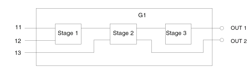
Multiple Stages Module
As described in the “Logic Gate Generator” section in this chapter, a primitive can have only one stage between input and output node. Under this condition, an XOR gate is not a primitive gate. For example, the following XOR gate has two stages.
The stage 1 rise delay R1, and fall delay F1, are calculated first. The second stages, R2 and F2 delays, are added to the first stage delays for total gate delay. For example
Rise Delay = F1 + R2
Fall Delay = R1 + F2
When there is more than one stage, the final delays are as follows:
Rise Delay = F1 + R2 +...+ Fn + Rn + 1
Fall Delay = R1 + F2 + R3 + F4...+ Rn + Fn + 1
This rule applies to all multiple stage devices. If there is a transfer gate, the on/off delays are added to both the rise and fall delay.
Multiple Output Devices
Where there is more than one output node, the delays at each output node are different because most logic simulators only let you specify one set of rise and fall delays. LPEPRO selects the worst case delays as gate delays. For example, the delays of gate G1 are the sum of delays in each stage, using the approach in the “Multiple Stages Module” section.
Cells With Internal Feedback Loop or Branch
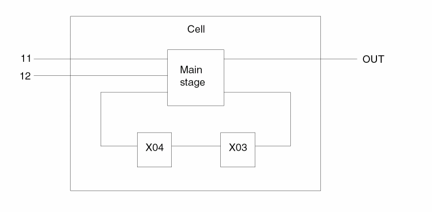
LPEPRO is not designed to handle complicated cells, so use primitive gates whenever possible. If the cell has an internal feedback loop or branch, delays of elements along the feedback loop or branch are added to the gate delay. For example, the delays of element X03 and X04 are added to the gate delay of this cell, using the formula in 1 above.
To avoid this, use the /GATE option to select the cells that have this problem. Because the W/L information of this type of element is known, you can calculate delay based on the capacitance of output nodes only, so that the delays are more accurate.
Reviewing Delay Information
Once the delays are calculated, scan them using the same approach you use to scan layout parameters. Use the TYPE, PRINT, or STORE command followed by DELAY to display delay information based on range, or the node name you specified. The delay command has the following options:
Checks the rise delay/fall delay ratio
Checks the fall delay/rise delay ratio
The /R/F option can be used to check pull-up/pulldown ratio.
Example 1
The following example checks any gate with a delay greater than 50 time units:
:TYPE DELAY > 50
Example 2
The following example checks pull-up/pulldown ratio and checks the ratio of rise delay to fall delay:
:TYPE DELAY/R/F < 1.5
In the following example, nodal capacitance is the same for both rise and fall delay. The R/F ratio in this case is the same as the pull-up/pulldown ratio.
CAL DELAY = (L/W)*C
Example 3
The following example checks delay of gates with output node A10, B10. LPEPRO prints the delay information of these gates only.
: TYPE DELAY A10, B10
The output listing contains the gate name, gate type, rise delay, fall delay, R/F ratio, and F/R ratio. An example of the output follows.
      *** DELAY INFORMATION ****
         *TYPE DELAY C3.2
C3.2   :  CXFR  R=76,  F=76,  R/F=1.00, F/R=1.00
C3.2   :  CXFR  R=4,   F=4,   R/F=1.00, F/R=1.00
Return to top