13
Operation Block Commands
Chapter 13 discusses the Operation Block Commands for Dracula in alphabetical order.
Introduction
This chapter describes the commands in the Operation block of your rules file. You can create as many Operation blocks as necessary to define your rules and processes. The preprocessor automatically concatenates the individual definitions in the order you specify.
The Operation block contains the following categories of commands:
- Logical Operations
- Electrical Node Extraction
- Sizing Operations
- Spacing Checks
- Circuit Element Extraction
- Electrical Rule Checking
- Layout Versus Schematic
- Layout Parameter Extraction
Logical Operations
The logical operation commands create new pseudo layers using combinations of original layers, previously created layers, and import layers. The maximum number of logical operation commands you can specify in a single rule deck is 3,000.
Electrical Node Extraction
The electrical node extraction commands define the connectivity between layers where the connection physically derives from the contacts. You define the layer sequence with the CONNECT-LAYER command in the Input-Layer block, and define the contacts that connect the specified layers in the Operation block.
Electrical nodes are formed by the layer processing sequence and the interlayer contacts. Dracula forms and uniquely labels each electrical node formed by the CONNECT-LAYER and CONNECT commands. This process is called stamping. You can carry the stamping information to newly generated layers in two ways:
- Dracula automatically stamps layers produced with the AND and NOT commands and stamps the output layer with the node label of the first layer (layer-a).
- The STAMP command stamps the node label from one layer to another. Stamping occurs only for stamped-layer polygons that are overlapped by nodes in the stamping layer.
Sizing Operations
The sizing commands let you alter the geometries in your database.
Spacing Checks
The spacing operations check geometric spacing and sizing on polygons in original and created layers and flag the errors. You can further process these errors using either conjunctive rules, the R option, or the R' option.
You use conjunctive rules to process the violations produced by prior checking commands. A conjunctive set is a series of commands that generates a single output. You invoke a conjunctive rule by placing an ampersand (&) at the end of a command line. The results of that command are then available to any command in the conjunctive set. Thus you can make a series of dependent checks.
An ampersand (&) generates error flags for the corresponding input layers. Flags for layer-a segments are marked on layer-a, and flags for layer-b segments are marked on layer-b. These are conjoined layers. Subsequent checks on a conjoined layer filter these errors until, if any remain, they are finally output. You can use the renamed conjoined layer in later checks, avoiding the need to recompute these error flags.
The ampersand (&) is a reserved character, and Dracula interprets anything following it on the same line as a comment. You cannot specify a command on the same line. Except for layers you rename, conjoined layers revert back to the original layer after the processing of the conjunctive rule is completed.
You can use the conjunctive rule to filter the error flags through the conjunctive set. The set always ends with an OUTPUT statement.
The maximum number of spacing commands you can have in a single rule deck is 3,000.
Circuit Element Extraction
The circuit element extraction commands define electrical circuit elements. You use these commands to extract MOS devices, pads, and electrical parameters such as widths and lengths. When you define electrical nodes with CONNECT commands, circuit element extraction commands automatically generate a circuit netlist. You can use this extracted circuit to perform electrical rule checks (ERC), layout parameter extraction (LPE), or layout versus schematic checks (LVS).
Dracula checks the devices defined in an ELEMENT command to verify that the devices are formed correctly. For terminals that are missing or not properly formed, Dracula reports the coordinates of the device in the .ERC file.
The first three characters you specify in an ELEMENT or PARASITIC command must be unique. You cannot specify the same layer name more than once in the ELEMENT command. The preprocessor checks this syntax.
Electrical Rule Checking
The electrical rule checking commands check for incorrect devices and gross continuity errors. You can apply some of these rules globally and some locally.
After completing your ERC checks, Dracula flags electrical nodes and elements as potential violations and generates graphic output. For electrical nodes, Dracula traces continuity through the contacts to all areas of layers with the same electrical potential. Dracula uses a definition area to identify elements. For example, the channel area can represent the MOS device to help locate particular violations.
Layout Versus Schematic
The layout versus schematic commands run Layout Versus Schematic (LVS), Layout Versus Layout (LVL), and Schematic Versus Schematic (SVS) comparisons.
Layout Parameter Extraction
The layout parameter extraction commands control parameter extraction and report layout parameters. These commands report layout parameters in SPICE-compatible formats with layout label cross-references. If you provide a schematic, LPE updates the source if it is in SPICE format. LPE reports in SPICE format with I/O and designator cross-references if the schematic netlist is in one of the logic simulation languages that Dracula accepts.
AND
AND{[D{n}]} layer-a layer-b trapfile {OUTPUT c-name l-num {d-num}}
AND[E] layer-a layer-b trapfile
Description
Creates a new layer from two other layers. The new layer consists of the region shared by the two layers.
Database partition functions were added for the SELECT, SIZE, and LOGICAL commands. These enhancements resolve capacity limitation issues with Dracula. This allows you to partition input layers of these functions into blocks. When you run Distributed Dracula, each block (pair) can be assigned to one processor. Specify a value between 2-10 inclusive following ‘D’ to indicate the number of partitions desired. The default value of ‘D’ is 4 if the value is omitted.
Arguments
Turns on the database partition feature
Number of blocks to be partitioned into
Name of the second input layer
The name of the trapezoid file created by the logical operation. Arguments layer-a and layer-b are order dependent and can affect the output trapfile if connectivity has been established. Electrical node information is automatically stamped on this output layer from layer-a after nodal information is set up on layer-a with the CONNECT command. The trapfile name can have up to seven characters and no special characters. A-Z and 0-9 are permitted, but the first character must be a letter.
Sends the results of the operation to an output cell.
C-name is the name of the output cell and can have six alphanumeric characters or fewer and no special characters. L-num is the cell layer number determined by your CAD system. If your c-name is rule03 and l-num is 5, the output cell name is rule0305.
The datatype number associated with the layer number (l-num) of the output cell. Use d-num for GDSII only. Values can range from 0 to 63.
Creates an edge information file for each generated layer. This information is used for sidewall capacitance extraction.
Examples:
AND ndiff poly ngate nsd
AND[D7] pdiff poly pgate psd
ANDNOT
ANDNOT layer-a layer-b ANDtrapfile NOTtrapfile
ANDNOT[E] layer-a layer-b ANDtrapfile NOTtrapfile
Description
Logical command to do AND/NOT at the same time. This operation simplifies the rule file.
Arguments
Name of the second input layer
The name of the trapezoid file created by the AND logical operation. Arguments layer-a and layer-b are order dependent and can affect the output trapfile if connectivity has been established. Electrical node information is automatically stamped on this output layer from layer-a after nodal information is set up on layer-a with the CONNECT command. The trapfile name can have up to seven characters and no special characters. A-Z and 0-9 are permitted, but the first character must be a letter.
The name of the trapezoid file created by the NOT logical operation. Arguments layer-a and layer-b are order dependent and can affect the output trapfile if connectivity has been established. Electrical node information is automatically stamped on this output layer from layer-a after nodal information is set up on layer-a with the CONNECT command. The trapfile name can have up to seven characters and no special characters. A-Z and 0-9 are permitted, but the first character must be a letter.
Creates an edge information file for each generated layer. This information is used for sidewall capacitance extraction.
Example
ANDNOT ndiff poly ngate nsd
ANGLED-EDGE-TOL
ANGLED-EDGE-TOL [=] {<value> | YES/ON | NO/OFF}
Description
This command enables and defines, or disables a tolerance setting for the DRC checking operation on non-manhattan edges.
For non-manhattan design, round-off issues are a well-known problem. This leads to a large number of "false" minimum DRC violations due to the snapping of vertices to a grid. For example, the user may start with a rectangle drawn at the minimum width of 1 um. This rectangle is then rotated by 30 or 45 degrees (or any angle that is not multiple of 90o). Due to snapping of the vertices to the grid, the resulting shape may have a width that is slightly less than 1um. This can lead to a "false" minimum width violation. ANGLED-EDGE-TOL sets the tolerance for the DRC operation in order to eliminate such false violations.
ANGLED-EDGE-TOL may be specified multiple times in a ruledeck. Every ANGLED-EDGE-TOL affects all DRC commands (EXT/ENC/INT/WIDTH) until either the end of the ruledeck or another ANGLED-EDGE-TOL command changes the setting. When it is inserted into the DESCRIPTION block it behaves the same as if it were the very first command in the OPERATION block.
Arguments
Turn tolerance on and set value to default 2 dbu.
Turn tolerance off. This is the default behavior.
Turn tolerance on and set tolerance to the specified value.
Example
*DESCRIPTION
...
RESOLUTION = 0.001 MIC
ANGLED-EDGE-TOL ON
...
*END
*OPERATION
...
; The following rule checks for metal pieces that are thinner than 0.18 um
; but for non-manhattan cases minimal metal width is 0.178 (0.18 - 0.002)
; as defined by the default 2 dbu setting of ANGLED-EDGE-TOL
WIDTH METAL LT 0.18 OUTPUT ERR 1 1
; The following rule changes the <value> of the ANGLED-EDGE-TOL
ANGLED-EDGE-TOL 0.001
; The following rule checks for metal pieces thinner than 0.18 um
; but for non-manhattan cases minimal metal width is 0.179 (0.18 -0.001)
WIDTH METAL LT 0.18 OUTPUT ERR 2 1
; The following rule disables the ANGLED-EDGE-TOL check
ANGLED-EDGE-TOL NO
; The following rule checks for metal pieces thinner than 0.18 um
; with no tolerance allowed for non-manhattan shapes.
WIDTH METAL LT 0.18 OUTPUT ERR 3 1
*END
AREA
AREAlayer-a{RANGE/NE/EQ/GE/GT/LE/LT}n1 n2{trapfile} [OUTPUTc-namel-num{d-num}]
Description
Performs a minimum area check. This operation checks polygons to determine if their areas are within an area range. It also creates layers that are within specified area boundaries.
Arguments
Flags polygons with areas such that n1 < AREA < n2. (Exclusive).
Reports an error if any value of the layer specified is not equal to the value you specify.
Reports an error if any value of the layer specified is equal to the value you specify.
Reports an error if any value of the layer specified is greater than or equal to the value you specify.
Reports an error if any value of the layer specified is greater than the value you specify.
Reports an error if any value of the layer specified is lesser than or equal to the value you specify.
Reports an error if any value of the layer specified is lesser than the value you specify.
Sends the results of the operation to an output cell.
C-name is the name of the output cell and can have six alphanumeric characters or fewer and no special characters. L-num is the cell layer number determined by your CAD system. If your c-name is rule03 and l-num is 5, the output cell name is rule0305.
Specifies the datatype number associated with the layer number (l-num) of the output cell. Use d-num for GDSII only; values can range from 0 to 63.
Example 1
AND poly diff gate
AREA gate RANGE 0 7 OUTPUT drc03 54
Example 2
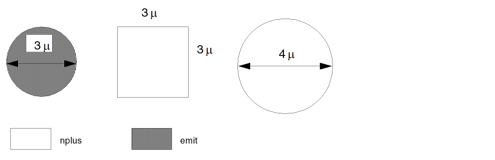
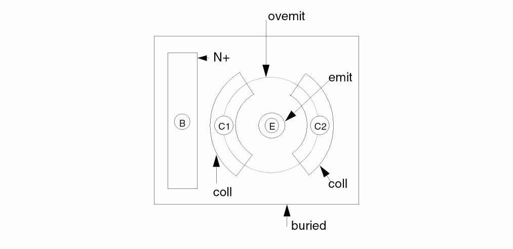
AREA nplus RANGE 7.04 7.08 emit
Finds the 3-micron diameter circle emitters in the nplus layer. You can use the emit layer for further operations.
ATTACH
ATTACHdevice-subtypeparameter-file{parset-name} {&}
Description
Joins source and drain parameters to the MOS or LDD devices. When you use this command with the NODE option of the LEXTRACT command, you can extract the source/drain parameters. Dracula reports the source/drain area in the SPICE output file as having a certain value.
In Dracula 4.81 and previous versions, using the ampersand (&) sign you could group ATTACH commands if the commands worked on the same device type. In those versions, the ATTACH command handled the extraction of common source or drain parameters of different subtype of devices belonging to the same device type using a syntax for example, as given below:
ATTACH MOS[A,B]
In this current Dracula (version 4.9), using the ampersand (&) sign, you can group ATTACH commands if the commands work on either the same device type, or shared common source or drain. So in this Dracula 4.9 version, along with the previous syntax for the same device type, the ATTACH command handles the extraction of common source or drain parameters of different device types grouped, using a syntax for example, as given below
ATTACH MOS[A] PDIFFN &
ATTACH MOS[B] PDIFFN &
ATTACH LDD[C] PDIFFN
Arguments
The device with subtype specified in the rules file. You can use a MOS or LDD device type. Multiple subtypes seperated by comma are also allowed in the same ATTACH command for source/drain parameters extraction of different subtype of devices which share common source/drain.
The file containing the source/drain parameters. You extract the source/drain parameters by using the LEXTRACT command with the NODE option.
The name of a parset (refer to the PARSET command) that specifies how the source and drain results are stored in the parameter file. The default is MOS.
Using the ampersand (&), you can group ATTACH commands if the commands work on the same device type.
Example 1
The following shows how you might use the ATTACH command in your run file:
*DESCRIPTION
...
PARSET TEST AREA PERI            ; PARSET FOR S/D
UNIT AREA,P PERIMETER,U
 ...
*END
...
*OPERATION
...
ELEMENT     MOS[N] NCHNL   METAL   DIFFN   OVPWELL ;N-CHANNEL
ELEMENT     MOS[P] PCHNL   METAL   DIFFP   NSUB    ;P-CHANNEL
...
LEXTRACT TEST DIFFN BY NODE PDIFFN
LEXTRACT TEST DIFFP BY NODE PDIFFP
ATTACH MOS[N] PDIFFN &
ATTACH MOS[P] PDIFFP
...
LPECHK
LPESELECT[S] MOS &
...
Example 2
The following shows a SPICE file with ATTACH command results:
Mxxx Nd Ng Ns Ns modelName L=4.5 μ W=20.0 μ AD=149.5P PD=59.0u
+ AS=139.9P PS=59.0u
Where AD, PD, AS, and PS are new keywords representing the areas and perimeters of the drain/source of the MOS transistors. Note that AS and PS are listed on a second line following the SPICE continuation sign (+) and that their values include units because the UNIT command was specified in the Description block.
Example 3
An example of using the ATTACH command to attach the AS/AD/PS/PD parameters to LDD devices:
*description block
; ...
PARSET   LDDS   AREA OVPR W L AS PS AD PD
PARSET   TEST   AREA PERI
*end
...
*operation block
...
; device gate drain source sub
; ------ ---- ------ ------ ----
ELEMENT LDD[XV] xvgate poly hvdiff stdiff psub
...
LEXTRACT TEST hvdiff BY NODE DRAIN
LEXTRACT TEST stdiff BY NODE SOURC
ATTACH LDD[XV] DRAIN &
ATTACH LDD[XV] SOURC
...
*end
Example 4
The following example shows devices of MOS type N and NH share common diffusion:
PARSET SD AREA PERI
......
ELEMENT MOS[N] NGATE POLY NSD PWELL
ELEMENT MOS[NH] NHGATE POLY NSD PWELL
........
LEXTRACT TEST NSD BY NODE PDIFFN
ATTACH MOS[N,NH] DIFFN
.....
ATTACH MOS[N] DIFFN &
ATTACH MOS[NH] DIFFN
ATTRIBUTE CAP
PARASITIC CAP {type}  layer-a  layer-b  layer-c
ATTRIBUTE CAP {type}  value-a  value-b
PARASITIC CAP {type}  layer-a  layer-a  layer-a
ATTRIBUTE CAP {type}  value-a1 value-b1
ATTRIBUTE CAP {type}  value-a2 value-b2
FRINGE CAP    {type} layer-a  layer-b
ATTRIBUTE CAP {type} value-a1 value-b1
ATTRIBUTE CAP {type} value-a2 value-b2
PARASITIC CAP {subType} device_layer terminal_layer1 terminal_layer2
ATTRIBUTE CAP {subType} areaCoeff perimCoeff depthRange
 sidewallCoeff
Description
Associates the geometry data of the PARASITIC CAP or FRINGE CAP functions with the corresponding process-dependent electrical properties. The ATTRIBUTE function does not accept units. The scale of the parasitic attribute must match the scale of the layout database. This function specifies four forms of parasitic capacitance.
- Case 1 is for area and perimeter capacitance.
- Case 2 is for same-layer fringe-field capacitance.
- Case 3 is for same-layer or different-layer fringe-field capacitance.
- Case 4 is for overlap capacitance with consideration of the fringe effect of the first terminal layer on the overlap capacitance.
Dracula supports piece-wise coefficients for fringe capacitors.
Arguments
The type code specified in the FRINGE CAP [type] device.
The capacitance per unit area between layer-a and layer-b. The value specified for value-a can be floating point (maximum of 7 digits) or a floating-point number followed by an integer exponent (maximum of 2 digits). When floating-point numbers are specified, the leading zeros are not counted in the 7-digit restriction. If the significant digits exceed the 7-digit limitation, the preprocessor rounds the value at the 7th digit. In scientific notation, the limit is 16 characters.
The capacitance per unit perimeter between layer-a and layer-b. The value can be a floating point number (maximum of 7 digits) or a floating-point number followed by an integer exponent (maximum of 2 digits). When floating-point numbers are specified, the leading zeros are not counted in the 7-digit restriction. If the significant digits exceed the 7-digit limitation, the preprocessor rounds the value at the 7th digit. In scientific notation, the limit is 16 characters.
The type code specified in the FRINGE CAP[type] device.
The maximum distance between two geometries of the same layer opposing each other where the fringe capacitance is analyzed.
The multiplier of the length of the edges under the maximum value a2.
The type code specified in the FRINGE CAP[type] device.
The maximum distance between two geometries of different layers opposing each other where the fringe capacitance is analyzed.
The multipliers of the length of the fringe edges under the value a1, a2 respectively.
Use this case to extract the primitive parameters TPR and CLL. You must specify depthRange and sidewallCoeff at the same time. Dracula evaluates the first terminal layer to calculate the possible fringe effect on the overlap capacitance. Therefore, the sequence of terminal layers is important.
Example 1
STAMP metpoly BY metal
PARASITIC CAP[X] metpoly metal poly
ATTRIBUTE CAP[X] 0.0005
The PARASITIC capacitor of type X forms between metal and poly conductor layers. The device layer is metpoly (metpoly = metal and poly).
The two connecting layers of capacitor terminals are metal and poly. Capacitance of type X is calculated using the following formula:
(area) × (0.0005)
Example 2
PARASITIC CAP[F] metal metal metal
ATTRIBUTE CAP[F] 6.0 0.0005
The PARASITIC capacitor of type F is for the fringe capacitance between metal lines. The device layer is metal, and both conductor layers are metal. The parasitic capacitance between metal lines is calculated for spacing distances up to 6 units, and the capacitance calculation is calculated by the following formula:
(projected metal length) x (0.0005) x (1/distance between metal)
Example 3
PARASITIC CAP[mp] metpol metal poly
ATTRIBUTE CAP[mp] 1E-18 1E-12
PARASITIC CAP[mp] metpol metal poly
ATTRIBUTE CAP[mp] .0005 .00012
PARASITIC CAP[mp] metpol metal poly
ATTRIBUTE CAP[mp] .0001234567E-9 .00007654321E-10
You can use two or more ATTRIBUTE functions to specify the piece-wise coefficients when handling the fringe capacitance. For example
PARASITIC CAP[EX] MET12 MET1 MET2
ATTRIBUTE CAP[EX] 0.5  1.2  0.2 0.032 ; PIECE-WISE COEFFICIENT
ATTRIBUTE CAP[EX] 0.5 1.2 0.6 0.019 ; PIECE-WISE COEFFICIENT
Example 4
In this case, two new reserved parameters, TPR and CLL, are added to the parameter set:
- TPR represents the perimeter where the device layer touches the projected edge of another geometry on the first terminal layer and has fringe effect with the first terminal layer.
- CLL is the sum of the fringe effect related to TPR. CLL is calculated as the current summation of all sidewallCoeff*TPR.
The default parameter set is as follows:
CAPO TPR CLL AREA PERI C
CAPO is the default name of the parameter set.
A different fringe coefficient is assigned to the parameter according to the depth between two geometries of the device layer and the first terminal layer, respectively.
The default equation for the capacitance calculation is
C = (areaCoeff* AREA)+ (perimCoeff*(PERI-TPR))+ CLL
You can also use the flexible LPE feature to define your own parameter set and equations for the parameter extraction. Your parameter set must include the TPR and CLL parameters. For example:
*DESCRIPTION
...
PARSET NEWE TPR CLL AREA PERI C ; parameter set for overlap
                                ; cap with fringe
*END
*OPERATION
PARASITIC   CAP[F]      M12 MET1 MET2
ATTRIBUTE   CAP[F]      0.5  1.2  0.2 0.019 ; PIECE-WISE COEFFICIENT
ATTRIBUTE CAP[F] 0.5 1.2 0.6 0.032 ; PIECE-WISE COEFFICIENT
LEXTRACT NEWE M12 BY CAP[F] PFILE & ; FLEXIBLE EQUATION
EQUATION C= 0.5*AREA +1.2*(PERI-TPR) + CLL
...
*END
For the following data, the value of TPR is TPR'+TPR'', but it is divided into sections when piece-wise fringe capacitance is considered. The value of the sidewallCoeff parameter depends on the separation between MET1 and M12.
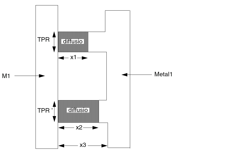
x1, x2, x3 = sep. betn MET1 and M12
If 0<x1<=.2, and .2<x2<=.6 and .6<
TPR = (TPR'+TPR'')
CLL = (0.032*TPR' + 0.019*TPR'')
C = 0.5*AREA +1.2*(PERI-TPR) + CLL
Example 5
In Example 4, when MET1 is cut-termed to extract parasitic resistance, you must specify the R option in the PARASITIC CAP command to ensure the correct extraction of TPR and CLL as shown in the following example:
CUT-TERM MET1 CONT M1RES M1TRM
STAMP M1TRM BY MET1
AND M1TRM MET2 M12T
AND M1RES MET2 M12R
PARASITIC[R] CAP[F1] M12T M1TRM MET2
ATTRIBUTE CAP[F1] 0.5 1.2 0.2 0.032
ATTRIBUTE CAP[F1] 0.5 1.2 0.6 0.019
PARASITIC[R] CAP[F2] M12R M1RES MET2
ATTRIBUTE CAP[F2] 0.5 1.2 0.2 0.032
ATTRIBUTE CAP[F2] 0.5 1.2 0.6 0.019
Example 6
You can specify 0 depth to the give a special coefficient for the co-linear fringe extraction. Currently the equation for the co-linear fringe is hard coded as C = K * WIDT.
FRINGE CAP[F]         M1  M2
ATTRIBUTE CAP[F]       0  2.5
ATTRIBUTE CAP[F]       1  4.5
ATTRIBUTE CAP[F]       2  1.5
ATTRIBUTE CAP[F]       3  0.5
The co-linear fringe will be calculated as C = 2.5 * WIDT.
Example 7
Both the zero and nonzero spacing fringe capacitance are calculated with the following equation.
*DESCRIPTION
...
ZERO-SPAC-F-EQU =YES
*END
*OPERATION
FRINGE CAP[A] ME1 ME2
ATTRIBUTE CAP[A] 0 1
ATTRIBUTE CAP[A] .5 1
LEXTRACT CAPF ME1 ME2 BY CAP[A] LCAPA &
EQUATION C = WIDT / SQRT((((3.205 + DEPT)**2.861/6.259)**2) + 57.5
*END
Example 8
Without this command, Dracula uses C=K*WIDT as the equation for zero spacing fringe capacitance and the following equation
C = WIDT / SQRT((((3.205 + DEPT)**2.861/6.259)**2) + 57.5)
for nonzero spacing fringe capacitance.
*OPERATION
FRINGE CAP[A] ME1 ME2
ATTRIBUTE CAP[A] 0 1
ATTRIBUTE CAP[A] .5 1
LEXTRACT CAPF ME1 ME2 BY CAP[A] LCAPA &
EQUATION C = WIDT / SQRT((((3.205 + DEPT)**2.861/6.259)**2) + 57.5
*END
ATTRIBUTE RES
ATTRIBUTE RES[type] sheet_res_value
{smashResValue maxResValue}
Description
Provides the process-dependent sheet resistance used to compute the resistance of the parasitic resistor devices defined by the associated PARASITIC RES command. The ATTRIBUTE RES command must follow a PARASITIC RES command having the same type parameter.
Checking Methods
Arguments
A two-character code that denotes the type of parasitic resistor device. The first character must be A-Z. The second character can be A-Z or 0-9, excluding 8. The second character is optional. Dracula uses this code to match this command with the associated PARASITIC RES command.
The sheet resistance value in units per square, where the units correspond to the resistance units specified in the UNIT command.
The resistance value used as a threshold. Series resistors with values below smashResValue are smashed.
The maximum value of a resistor that results from smashing serial parasitic resistors. This prevents creating a big resistor from subsequent smashing.
Example
In this example, LPE extractions of parasitic resistance values made from PRES are computed using the sheet resistance value .01 Kohms/square. Dracula smashes resistors with values below 10 and does not create any resistor with a value greater than 200.
*DESCRIPTION
UNIT = CAPACITANCE,PF AREA,U PERIMETER,M RESISTANCE,K
*OPERATION
PARASITIC RES[P] PRES PTRM
ATTRIBUTE RES[P] .01 10 200
BBOX
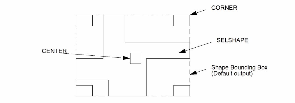
BBOX inLayer {CENTER {size}/SELSHAPE/CORNER {size}/RELATIVE ratio/WHOLELAY} {PRESERVE} {WARN} {NOT} {WIDTH relation wid1 {wid2}} {LENGTH relation len1 {len2}} {RATIO relation rat1 {rat2}} trapfile {OUTPUT c-name l-num {d-num}}
Description
Creates enclosing bounding boxes for shapes on the specified input layer, and outputs one of the following five possible outputs for shapes whose bounding box dimensions fall within the specified length and width ranges:
- Bounding boxes of the original shapes (the default output)
- The input shapes
- Center marker of the bounding box
- Corner markers of the bounding box
- One rectangle which represents the whole layer BBOX
The following figure shows the four possible outputs of the BBOX command:
Figure 13-1 The four possible outputs from the BBOX command
Arguments
|
Optional argument that outputs a marker at the center of the shape’s bounding box instead of a bounding box. Figure 13-2 illustrates the exact location of the center marker. |
|
|
Optional argument that outputs the original input layer shape to the specified trapezoid file instead of bounding boxes. This is useful to perform the shape filtering based on bounding box size. |
|
|
Optional argument that outputs markers at the corners of the shape’s bounding box instead of a bounding box. |
|
|
Optional marker size value that applies to the
If you do not specify a marker size value for the
CENTER argument, the default value of 6 DBU (i.e., 6*RESOLUTION) is used. A marker size value of 5 DBU is used if there is a 0.5 DBU difference between the center marker and the center of the bounding box. If you do not specify a marker size value for the CORNER argument, the default value of 5 DBU (i.e., 5*RESOLUTION) is used. |
|
|
Optional argument which works similar to |
|
|
Shows the relative size of markers in comparison to bounding box size. |
|
|
Optional argument that allows to generate one rectangle per layer which represents the whole layer bounding box. |
|
|
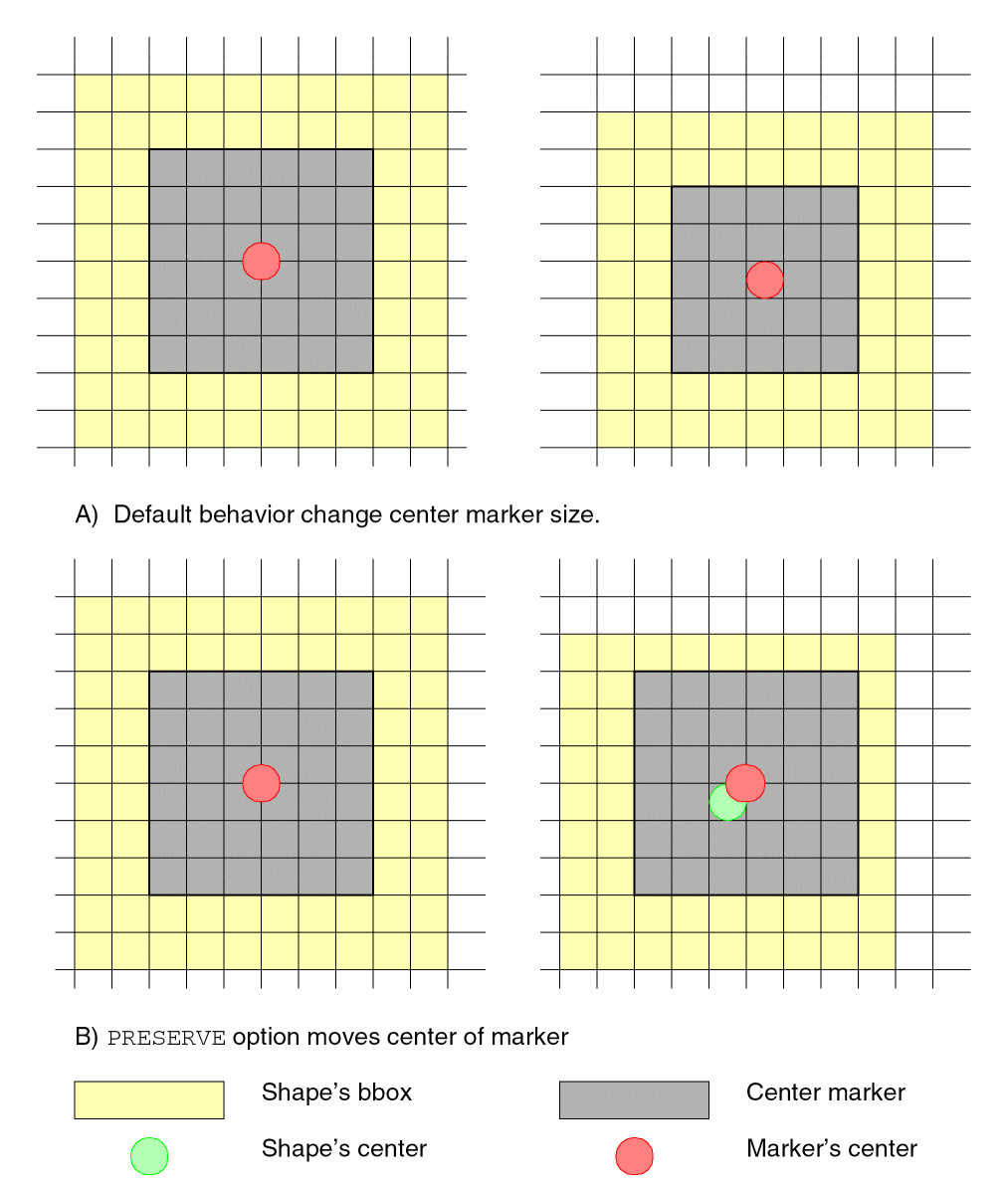
Optional argument that allows you to preserve the size of center markers regardless of whether the center of a shape is on-grid or not. In the case where the center point is off-grid, the center of the marker will be shifted to the nearest on-grid point. Figure 13-3 illustrates how this option works. |
|
|
Optional argument to output warning messages in case of the marker size value was modified because the shape’s center marker is off-grid. If the |
|
|
Optional argument that outputs only bounding boxes that do not satisfy the specified |
|
|
Optional arguments to specify the width and length constraints to the |
|
|
Optional argument to specify BBoxes selection by their |
|
|
Relation operators for applying the |
|
|
Specifies the |
|
|
Sends the results of the command to the output cell. |
Figure 13-2 Location of Center Markers
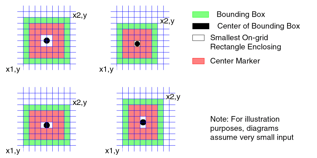
Figure 13-3 How PRESERVE keyword works
Example 1
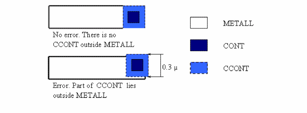
The following example checks that the contact center should be a maximum distance of 0.15um to the metal edges.
BBOX CONT CENTER 0.3 CCONT
NOT CCONT METALL BADCONT OUT ERR 1
Example 2
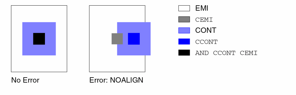
The following example checks that the contact must lie in the center of the emitter.
BBOX CONT CENTER CCONT
BBOX EMI CENTER CEMI
XOR CCONT CEMI NOALIGN OUT ERR 2
Example 3
The following examples uses METALL1 bounding box to define chip working area and defines all the rest area of chip as test area.
BBOX METALL1 WHOLELAY METBBOX
SIZE METBBOX by 1 CHIPBBOX
NOT BULK CHIPPBOX TESTAREA
Example 4
The following example checks that via layer of M1 to M2 connection covers at least most internal 50% of area M1 and M2 overlaps.
AND M1 M2 M1M2OVR
BBOX M1M2OVR RELATIVE 0.5 TMP
NOT VIA1_2 TMP BADVIA
Example 5
The following example selects all contacts with their length more than width*3.
BBOX CONT RATIO GT 3 LONGCNT
*BREAK
*BREAK name
*BREAK label shell_command {\|&}
Description
Specifies the break points for a RESTART operation, or executes a portion of a job. Use this command in the Operation block only. This command is preceded by an asterisk (*).
You cannot insert a *BREAK command between any of the following command groups: DEVTAG, EQUATION, LPECHK, LPESELECT, or LVSCHK. For example, you cannot insert a *BREAK command between two or more EQUATION commands. PDRACULA issues a warning message if you insert a *BREAK command between any of these commands.
Arguments
The name you specify. The name can be of 1-16 alphanumeric characters (A-Z and 0-9). The first character must be a letter.
You cannot use the following reserved names with *BREAK: BEGIN, EXPAND, SORT, MERGE, SYSOUT, DELETE (if KEEPDATA = NO or SMART), END, GENENV, REGION, LVSCHM, SCHMIN, and LVSNET. These reserved names are internal break points found in the PDRACULA Job Control Language (JCL). You can use these points to restart a job.
When running an LVS job, you can use the following reserved break points: LVSNET, SCHMIN, and LVSCHM.
Either a start or end point for the *BREAK command. Use this only when specifying shell commands.
The names of the shell commands to be executed at this break. You can specify multiple lines by using the ampersand (&) at the end of each line. You can use the backslash (\) to divide a single line into two lines if the length of the line is longer than the limitation.
Example 1
This example reruns a short check job. Remember, to restart a job, specify the KEEPDATA = YES command in your run file.
*OPERATION
.
*BREAK SHORTCHK
MULTILAB OUTPUT SHORTS10
*END
Example 2
This example specifies start and end points for the *BREAK command.
*OPERATION
.
*BREAK START1 if( $mode == ’FLATTEN’ || $mode == \
’COMPOSITE’|| $mode == ’HIER’) then &
echo "RUN_MODE = $mode"
NOT AAA BBB CCC
 .
 .
*BREAK END1 endif
Example 3
This example specifies an ‘if then’ statement embedded in the shell commands.
*BREAK START if( $run == ’now’) then &
echo "run_mode = $run" &
endif
CALCULATE
CALCULATE RATIOFILE parExpression
Description
Calculates the parameter ratio of each node among multiple layers. This command is an extension of the COMPUTE command, which only applies to limited layers with limited operation. To check the “antenna effect,” you must specify this command in addition to the LEXTRACT and CHKPAR commands.
Arguments
Output file used as the input file for the CHKPAR command. Contains the ratio of parameter values calculated from the equation specified in the command for each node. Use CHKPAR PAR to check the result.
The parameter expression can be one of the following:
Example 1
CALCULATE RATIO1=PNGATE / PGATE
CALCULATE RATIO1=SUM.PNGATE.AREA /SUM.PGATE.AREA
PNGATE and PGATE are the parameter files from the previous LEXTRACT commands. For each node in the PNGATE file, the area is calculated. The same calculation is done for the PGATE file. Then, the ratio is calculated per node. Nodes that do not exist in all parameter files are set to zero.
CALCULATE RES2 = (MIN.PNGATE + c1*MAX.PM1) / PGATE
CALCULATE RES2 = (MIN.PNGATE.AREA + c1*MAX.PM1.AREA) / PGATE.AREA
CALCULATE res3= (MAX.PNGATE.PERI+c1*SUM.PM1.AREA+c2*MAX.PM2.PERI)/
MAX.PGATE.AREA
Example 2
PARSET ANT AREA PERI
...
LEXTRACT ANT GATE BY NODE PGATE
LEXTRACT ANT NGATE BY NODE PNGATE
LEXTARCT ANT M1 BY NODE PM1
LEXTRACT ANT M2 By NODE PM2
CALCULATE RATIO1 =
PNGATE / PGATE
CALCULATE RATIO1 =
SUM.PNGATE.AREA /SUM.PGATE.AREA

CALCULATE res2 =
MIN(SUM.PNGATE,0.84*SUM.PM1) / PGATE
CALCULATE res2 =
MIN(SUM.PNGATE.AREA,0.84*SUM.PM1.AREA)/SUM.PGATE.AREA

CALCULATE res3 =
(MAX.PNGATE.PERI+0.2*SUM.PM1.AREA+0.7*MAX.PM2.PERI)/MAX .PGATE.AREA
CAT
CAT lay1 lay2 lay3 ... layN PseudoTrapFile
CAT[ M ] lay1 lay2 lay3 ... layN TrapFile
Description
Lets you quickly merge several layers while conveying nodal information, if present, in all of the input layers.
Arguments
Output layer created by the CAT command.
Output layer created by the CAT command.
Option that produces a merged trapezoidal file.
The CAT command without the [M] option produces a pseudo trapezoidal file that contains sorted but unmerged trapezoids. This file can be used as an input layer for CAT or OR commands only.
Example 1
This example shows the merging of 4 layers— M1, M2, M3, and M4— into layer RES.
CAT[M] M1 M2 M3 M4 RES
Example 2
This example shows the merging of 12 layers— M1, M2, M3, M4, M5, M6, M7, M8, M9, M10, M11, and M12— into layer RES.
CAT[M] M1 M2 M3 M4 M5 M6 M7 M8 M9 M10 M11 M12 RES
Example 3
This example shows the merging of 15 layers— M1, M2, M3, M4, M5, M6, M7, M8, M9, M10, M11, M12, M13, M14, and M15— into layer RES. Use two CAT commands; only the last should contain the [M] option.
CAT M1 M2 M3 M4 TMPL
CAT[M] TMPL M5 M6 M7 M8 M9 M10 M11 M12 M13 M14 M15 RES
Example 4
This example shows the merging of 40 layers— M1, M2, M3, M4, M5, M6, M7, M8, M9, M10, M11, M12, M13, M14, M15, M16, M17, M18, M19, M20, M21, M22, M23, M24, M25, M26, M27, M28, M29, M30, M31, M32, M33, M34, M35, M36, M37, M38, M39, and M40— into layer RES. Use four CAT commands; only the last should contain the [M] option.
CAT M1 M2 M3 M4 M5 M6 M7 TMPL1
CAT M8 M9 M10 M11 M12 M13 M14 M15 M16 M17 M18 M19 TMPL2
CAT M20 M21 M22 M23 M24 M25 M26 M27 M28 M29 M30 M31 TMPL3
CAT[M] TMPL1 TMPL2 TMPL3 M32 M33 M34 M35 M36 M37 M38 M39 M40 RES
CHKPAR
CHKPAR [option]infile {layer-a} relation value1{value2} [{outlayer} {OUTPUTc-name l-num{data-type}]
Description
Selects a group of nodes from the result of a COMPUTE command, and under certain conditions, outputs the layer. This is one of the commands you use for an antenna check. For more information about antenna checks, refer to Chapter 7, “Extracting Electrical Parameters (LPE),” or the LEXTRACT command description in this chapter.
CHKPAR outputs to the log file the node numbers and ratio values for the violated nodes so you can determine the severity of the violation. You set the number of nodes to output by specifying the LISTERROR command in the Description block. If you specify LISTERROR = YES, the first 100 nodes that satisfy the condition are output. This is the default setting for CHKPAR. If you specify LISTERROR = NO, the nodes are not output. You can also specify the number of nodes to output with the LISTERROR command.
Arguments
Checks the computed AREA ratio or the result from the CALCULATE command.
Checks the computed AREA value or ratio.
Checks the computed perimeter value or ratio.
Name of the output file from a COMPUTE command.
Name of the output layer. It must carry nodal information. If this is not specified, all connect layers will be examined.
One of the following operations:
Value for the relation operation.
Upper limit for the RA operation.
Name of the output layer file.
Name of the output cell containing geometric results from the operation. This cell name cannot be more than seven characters.
Layer number of the output cell.
Datatype associated with the l-num of the output cell.
Example
*DESCRIPTION
.
.
LISTERROR = YES ; lists the first 100 node violations in
;          ; the log file
.
.
*END
.
.
*OPERATION
.
.
LEXTRACT ANTE FIELD BY NODE ANTEN1
LEXTRACT ANTE GATE BY NODE ANTEN2
COMPUTE MIN ANTEN1 OUT1
COMPUTE MIN ANTEN1 ANTEN2 OUT2
CHKPAR A OUT1 POLY GT 1500 OUTPUT LONG 1
CHKPAR P OUT1 POLY GT 1500 OUTPUT LONG 2
CHKPAR A OUT2 POLY GT 25 OUTPUT WRONG 1
CHKPAR P OUT2 POLY GT 10 OUTPUT WRONG 2
.
.
*END
COEFFICIENT CAP
COEFFICIENT CAP[type] value-a value-b value-c value-d
Description
Associates the sidewall-up/down/colinear data coming from the NOT[E], AND[E], and PARASITC CAP commands with the process-dependent capacitance coefficients.
After using at least one of the NOT[E], AND[E] operations to extract capacitance sidewall information of deviceLayer, you can use COEFFICIENT CAP to gather this information for the cap. Without any NOT[E], AND[E] operation rules for the deviceLayer, it is illegal to write COEFFICIENT CAP for that device.
Arguments
The type specified in PARASITIC CAP[type] device.
Capacitance per unit sidewall up perimeter.
Capacitance per unit sidewall down perimeter.
Capacitance per unit colinear edge perimeter.
Example
AND[E] M1T METAL2 M12
...
PARASITIC CAP[SW] M12 M1T METAL2
COEFFICIENT CAP[SW] 0.3 0.4 0.23 0.44
COMPUTE
COMPUTE action par-file1 [par-file2 {par-file3}] outfile
Description
For each node, calculates the value and ratio of the geometric parameters that you extract with the LEXTRACT command. When there is only one parameter file, Dracula calculates the value. When there are two or three parameter files, Dracula calculates both the value and the ratio. The AREA and PERI parameters are currently supported.
For more information on using the COMPUTE command for antenna checks, see “Extracting Area Ratios using the COMPUTE Function” section in the “Writing Rules for Dracula” chapter of the Dracula User Guide.
Arguments
Is one of the following values:
Specifies the total area of all regions on the same node for each par-file, then calculates the ratio of the first result over the minimum of the second and third results on the same node.
Layer to compare. It must be an output file from the LEXTRACT command.
Layer to compare. It must be an output file from the LEXTRACT command.
Layer to compare. It must be an output file from the LEXTRACT command. This layer is required only if you specify mingate.
Name of the output file for the COMPUTE command. This is the input file for the CHKPAR command. Do not use more than seven characters in this file name.
Example 1
DESCRIPTION
PARSET ANTE AREA PERI
*END

LEXTRACT ANTE FIELD BY NODE ANTEN1
LEXTRACT ANTE GATE BY NODE ANTE2

COMPUTE MIN ANTEN1 OUT1
COMPUTE MIN ANTEN1 ANTEN2 OUT2

CHKPAR A OUT1 POLY GT 1500 OUTPUT LONG 1
CHKPAR P OUT1 POLY GT 1500 OUTPUT LONG 2

CHKPAR A OUT2 POLY GT 25 OUTPUT WRONG 1
CHKPAR P OUT2 POLY GT 10 OUTPUT WRONG 2
Example 2
LEXTRACT ANTE PLY2NG BY NODE ANTEN1Note:
LEXTRACT ANTE NG BY NODE ANTEN2
LEXTRACT ANTE PG BY NODE ANTEN3
COMPUTE MINGATE ANTEN1 ANTEN2 ANTEN3 ANTOUT CHKPAR A ANTOUT FPOLY2 GT 100.0 OUTPUT D513A 20
CHKPAR PAR OUT2 POLY GT 25 OUTPUT WRONG 1
CHKPAR A OUT2 POLY GT 25 OUTPUT WRONG 1
CONNECT
CONNECTlayer-a layer-bBYcont-layer
Description
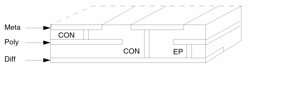
Defines interlayer connectivity; that is, connects two layers by a set of contacts. For more information about connectivity, refer to the CONNECT-LAYER section in Chapter 12.
Arguments
The previously defined layer that consists of the contacts that connect layer-a to layer-b. Cont-layer must have at least three characters, and the first three characters must be unique. The fourth character must be a letter, although the name can contain numeric characters (cont1 is allowed, but con1 is not). The preprocessor assigns the highest priority layer as the master layer. Cont-layer can connect only from the master layer to any other layer.
Example
CONNECT metal poly BY cont
CONNECT metal diff BY cont
CONNECT poly diff BY epi
CONNECT poly diff BY cont ; (not allowed)
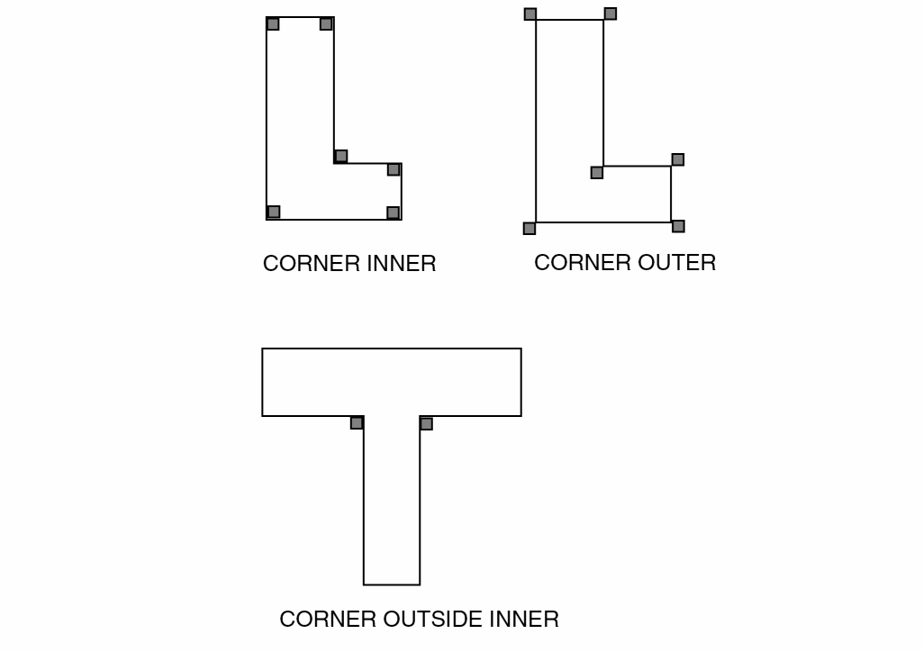
CORNER
CORNER{[option]}layer-a [relation-a] [relation-b] {{NOT} LT/GT/RANGE ang1 {ang2} } {CORNER-SIZE n} output-layer {OUTPUT c-name l-num {d-num}}
Description
Recognizes polygon corners and reports them to the specified output layer for special DRC checking.
Arguments
If you do not specify any options, this command works for Manhattan angles.
INSIDE or OUTSIDE. INSIDE creates a rectangle the size of CORNER-SIZE on the inside of shapes. OUTSIDE creates a rectangle the size of CORNER-SIZE at all corners on the outside of shapes.
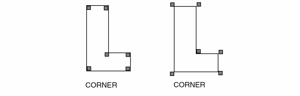
INNER or OUTER. INNER creates a rectangle the size of CORNER-SIZE on the inside edge of all corners. OUTER creates a rectangle the size of CORNER-SIZE on the outside edge of all shapes.
{NOT} [ LT | GT | RANGE ] ang1 {ang2}
This operation flags only corners whose angle matches the given constraint (see Examples 4 and 5 for details). If the keyword RANGE is specified, a second angle (ang2) must also be used.
Corner size in user units (n). If you do not specify this option, the default value is 2 times the resolution unit. If you specify a corner size of one resolution unit, round-off might occur at non-Manhattan corners. Dracula issues a warning if you specify a corner size of one resolution unit.
Sends the results of the operation to an output cell.
C-name is the name of the cell and can have six alphanumeric characters or fewer and no special characters. L-num is the layer number determined by your CAD system.
The datatype number associated with the layer number (l-num) of the output cell. Use d-num for GDSII only. Values can range from 0 to 63.
Example 1
The following example reports Manhattan angles and creates a rectangle of the inside edge of all shapes and corners. The output is sent to SUB001.
CORNER ME1 INSIDE INNER SUB001
Example 2
This example reports Manhattan angles and creates a rectangle of .03 microns at all corners on the outside of shapes. The output is sent to SUB002.
CORNER ME1 OUTSIDE INNER CORNER-SIZE .03 SUB002
Example 3
This example reports 90 degree angles and creates rectangles on the inside edge of all shapes and corners. The output is sent to SUB004.
CORNER[A] ME1 INSIDE INNER SUB004
Example 4
The following checks all acute angles within a tolerance of one degree:
CORNER MET LT 89 out acute 1 0
Example 5
The following gets all 45 and 315-degree corners (but not 135 and 225) and writes them to layer COR1 for further processing:
CORNER RA 44.5 45.5 COR1
COVERAGE
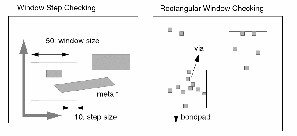
COVERAGE {NOT} input-layer [LT/LE/GT/GE/RA] per1 {per2} windowSize stepSize {CENTRIC} {OUTSQU square-file} {SQSZ size-of-squares}
{BOUND boundary-layer}{trapfile}
{OUTPUT c-name l-num }
COVERAGE {NOT} input-layer [LT/GT/RANGE] per1 {per2} [RECT rectangle-layer/BASLAY base-layer] {trapfile} {OUTPUT c-name l-num }
COVERAGE {NOT} input-layer [LT/GT/RANGE percentage windowSize stepSize MIN-RATIO minRatio BOUND boundary-layer {trapfile} {OUTPUT c-name l-num
{d-num}}
Description
Dracula reports an error if the area surrounding a specified point in the layout is not covered by a specified area percentage.
This command is intended for flat mode only. If you use it in a hierarchical mode, the input layers must be flattened.
In version 4.81 and later versions, Dracula supports region-based density check to implement the process rules in finding the via and bent gate density. In the 4.7 and previous versions of Dracula, you could not implement such rules as only window-based check was supported.
Given below is a T-shaped area over which is an O-shaped area and region-based density check allows you to do a density check of the O-shaped area.
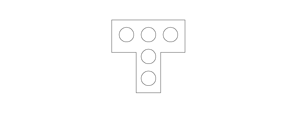
A region-based density sums up all the O shape area which is then divided by the T shape area, that is,
O shape density over T shape = ( sum of O shape areas within T shape ) /
                ( T shape area )
Checking Methods
Flat and hierarchical (internally flattened)
Arguments
Specifies the input layer name
The coverage rate is less than or equal to the percentage.
The coverage rate is greater than or equal to the percentage.
The coverage rate is between per1 and per2.
Specifies the window size in each step of the coverage check. The windowSize must be a multiple of stepSize.
Specifies the step size value to be used.
A new option added to Dracula 4.81 and subsequent versions. This option defines the central location of squares reported into the trapfile and/or output, relative to the violating window. If you don’t specify this option, the trapfile and/or output will contain the entire merged violating windows. The “Example 11 - Example for the CENTRIC Option” section provides more information.
This enhancement lets you have the possibility to obtain the results of the COVERAGE operation in Dracula verification in an equivalent form to that of Assura verification.
Specifies the layer created by the SIZE operation. The output-layer can have up to seven characters and must have no special characters. You can use A-Z and 0-9, but the first character must be a letter.
Writes the step squares in the violating window that has ratio within the percentage as a trapezoid file.
The size of squares in square-file.
If you don’t specify this parameter, the size of the squares is the same as the window step size.
Keyword used to specify the minimum area occupied ratio of the boundary layer in one check window to trigger the checking while doing density check.
Specify the minimum area occupied ratio of the boundary layer in one check-window to trigger the checking. If the area occupied ratio of boundary-layer in the check-window is less than the minRatio, the check-window will be ignored and Dracula will report the relative information to the log file; otherwise, Dracula will calculate the density based on the “overlap region” of check-window and the boundary-layer and output the violating check-window. See “Example 10 - Example for minRatio” in this section for more information.
Keyword used to specify boundary layer while doing density check.
Trapfile with rectangle(s) which define the boundary of the COVERAGE check. The boundary can be larger or smaller than the primary cell boundary. You can specify multiple rectangle in the trapfile. COVERAGE will do the check in each rectangle one by one.
Output layer with trapezoid file formats. It can be used as input layer by the subsequent commands.
Sends the results of the operation to an output cell.
Is the name of the cell and can have six alphanumeric characters or fewer and no special characters.
Is the layer number determined by your CAD system.
Region-based density checking within the constraints of a rectangular shape. For each rectangle in the rectangle-layer, Dracula computes this equation:
ratio = (area of shapes inside rectangle) / (area of rectangle)
Supports only the layer with rectangular shapes
For each region in the base layer, COVERAGE computes this equation:
density ratio = (area of shapes inside the region/(area of the region)
Base-layer supports the layers with any kind of shapes.
Output ratio not in the range.
Example 1
This example configures the chip as a grid with a step of 10 microns and reports an error if the surrounding 100x100 micron square area of a specific grid point is not covered by an area percentage of 60 percent.
COVERAGE POLY LT 0.6 100 10 POLYERR
Example 2
COVERAGE METAL LT 0.5 100 10 METALC1
Example 3
COVERAGE metal1 LT 0.3 100 10 merr1
X Y Ratio
------------------------
100 .23   924.34  0.2
102.5     123.52  0.15
Example 4
COVERAGE metal1 LT 0.3 50 10 OUTPUT merr 1
Example 5
COVERAGE via LT 0.05 RECT bondpad OUTPUT viabond 1
For each bond pad area, computes this equation:
ratio= (area of vias inside bondpad)/ (area of bondpad)
If the ratio is less than 0.05 the Dracula software reports it.
Example 6
COVERAGE metal LT 0.32 100 20 OUTSQU spa_met SQSZ 18 OUTPUT err 1
SIZE metal by 4 tt1
NOT spa_mnet tt1 fsqu OUTPUT fillsqu 1
The above example uses OUTSQU to fill the empty slots of the metal layer. The gap between each fill square is 2u(20u-18u). The filling squares are 4u away from the original metal.
Example 7
(Checking and generate rectangles for area filling)
SIZE BULK by 2.0 mybound
COVERAGE metal LT 0.2 50 10 BOUND mybound ERRWIN
GENRECT errwin XYLEN 2.0 3.0 XYGAP 1.0 1.2
(GENRECT generates rectangles that overlap the input layer and would also like to fill the area outside the cell.)
BULK is already oversized by 1 u from cell area. In the above example, the checking boundary is totally oversized from cell area by 3.0 u.Example 8
COVERAGE met2 LT 0.2 50 10 BOUND cframe output err 1
Example 9
Given below is an example of range-based density check.
COVERAGE O-trapfile LT 0.3 BASLAY T-trapfile itrapout OUTPUT merr 1
Example 10 - Example for minRatio
COVERAGE met1 LT 0.6 100 50MIN-RATIO30BOUNDmetbound OUTPUT meterr 0 0
Dracula first checks the area occupied ratio of this check-window:
area occupied ratio= ( 75x100 / 100x100 ) = 75 % >minRatio= 30 %
Thus, it continues to check the density for this check-window:
density = area of input layer inside the boundary-layer / area of overlap region
= ( 75x50 / 75x100 ) = 50 %
Dracula finally outputs the violating check-window into the output layer.
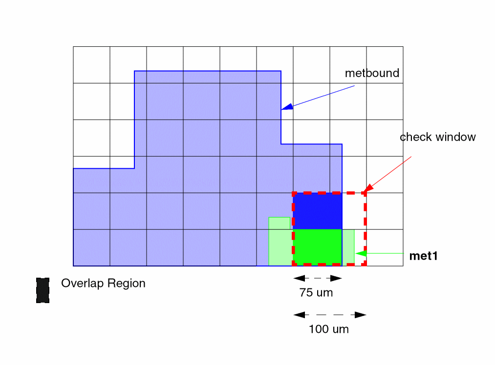
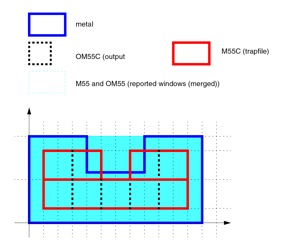
Example 11 - Example for the CENTRIC Option
SIZE BULK BY 4 OM
COVERAGE METAL GE 0.55 4 2 BOUND OM M55 OUTPUT OM55 0 0
COVERAGE METAL GE 0.55 4 2 CENTRIC BOUND OM M55C OUTPUT OM55C 0 0
CUT
CUT{[STRIP]} layer-a {layer-b} trapfile
Description
Cuts out geometries and uses them to generate a new layer for PRE. The CUT command does not cut polygons, so you must convert all polygons to trapezoids before using the CUT command.
You can use the resistor recognition layer as a terminal layer, but you cannot use layers derived from the resistor recognition layer as a terminal layer.
Checking Methods
Arguments
Produces a one-resolution-unit wide strip on opposite edges of any rectangular angle on layer-a. Dracula forms the strip on the inside of the trapezoid being cut. Use the STRIP option only on rectangular geometries.
The layer whose trapezoids are to be cut.
Use with the STRIP option. In the case of parasitic resistors, this layer typically corresponds to the resistor terminal layers generated so far. This layer guides the strip cuts in a direction perpendicular to the flow of current.
The trapezoid file created by the CUT command. The trapfile consists of trapezoids cut from layer-a that satisfy the condition.
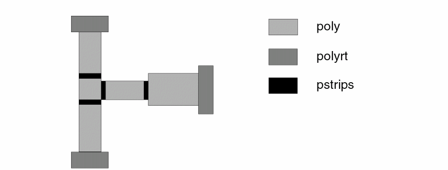
CUT-TERM
CUT-TERMcond-layer cont-layer res-layer term-layer{term-dev} {MAXNS=length} {MAXWIDTH=width} {ALIGN=YES/NO} {45CORNER=compenFactor}
CUT-TERM[P]cond-layer cont-layer res-layer term-layer{term-dev} {MAXNS=length} {MAXWIDTH=width} {ALIGN=YES/NO} {45CORNER=compenFactor} {WLRATIO=value}
Description
Generates a resistor body layer and a resistor terminal layer from a conduction layer and a contact layer. PRE uses the output resistor body and terminal layers to compute parasitic resistance and capacitance.
The CUT-TERM command cuts the following elements:
-
Contact terminals
Cuts contact regions from the resistor layer. -
Junction terminals
Cuts junction areas from the resistor layer. A junction is a 90-degree corner, a T-junction, or a cross-shaped junction. -
Long wires
Cuts long geometry strips into smaller segments. A long strip geometry is more accurately represented as a series of RC lumped circuits.
CUT-TERM replaces a series of commands previously required to achieve similar results. CUT-TERM is the preferred method for new rules files because it produces more accurate results. However, you can still use the old commands instead of CUT-TERM. For a sample listing of the commands CUT-TERM replaces, refer to the following “Example” section.
Checking Methods
Arguments
Name of the conduction input layer.
Name of the contact input layer.
Name of the resistor body output layer.
Name of the resistor terminal output layer.
All device terminal layers belonging to cond-layer.
Maximum length of a parasitic resistor device specified as a number of squares. If a resistor exceeds the number of squares you specify (MAXNS), the resistor is partitioned into multiple devices evenly.
Each resistor devices formed is smaller than the MAXNS value, and the values are distributed evenly on the resistor. The maximum difference between two sections is 1. For example, if the resistor body is 91, and you specify a MAXNS value of 20, the sections are 19, 18, 18, 18, 18.
Value used by the WIDTH command within the command sequence that CUT-TERM executes. The default width is 40. For an example of how CUT-TERM uses MAXWIDTH=value in the WIDTH command see Example 1 below.
If you specify ALIGN=YES, CUT-TERM forms the contact terminal at the alignment edge of the conduction layer and the contact layer. The edge of the terminal layer aligns with the contact as shown below.
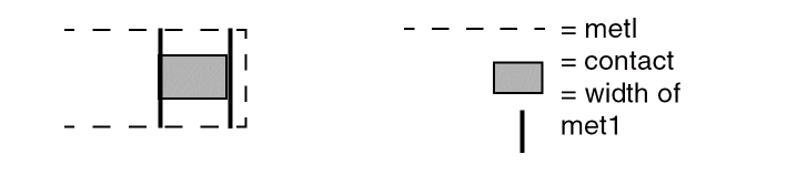
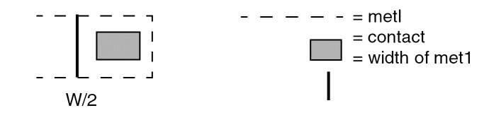
If you specify ALIGN=NO (or, if you do not specify the ALIGN argument), the terminal layer is formed by extending one-half the width of the conduction layer from the contact as shown below.
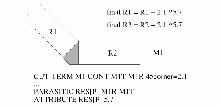
The number of square to be added as resistance compensation for a 45 degree terminal. The final compensation value will be equal to (sheetResistance*compenFactor). For example, the following layout, the extracted resistance will be,
This option is only available for use with the CUT-TERM[P] option, which enables creating resistor body and terminal layers when the ratio of the width over the length is less than or equal to the specified value (W/L <= WLRATIO). The default value for WLRATIO is 1.
Option [P]
The CUT-TERM[P] option supports improved accuracy of parasitic resistor layer cutting for special circumstances. This results in more accurate calculation of the resistor value.
1.) When there is a conducting layer with two contacts and they are placed near the longer side (see below).
When the width is greater than the length (W>L) only the terminal layer is created. Using the CUT-TERM[P] option enables creating both the resistor body layer and a resistor terminal layer in these cases.
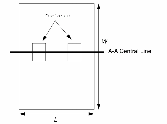
2.) In the following case, the width is greater than the length so only the terminal layer is created for the center piece of the conductive layer below.
Using the CUT-TERM[P] option enables creating the resistor body layer and terminal layer for each layer.
You should use the CUT-TERM[P] option only when there are no ’X’ or ’T’ connections of metal lines on the layers. In this case wide resistors will be just wide resistors.
Example 1
CUT-TERM R_IN C_IN R_OUT T_OUT T_DEV MAXNS=20 MAXWIDTH=50
This runs the following command sequence in flat mode. Angle brackets (<>) surround temporary file names. An asterisk (*) indicates internal modules used by CUT-TERM.
*PXCONT R_IN C_IN <TX>
 OR <TX> <TX> <T1>
 NOT R_IN <T1> <R1>
*PXJUNC R_IN <TX>
 OR <TX> <TX> <T2>
 NOT <R1> <T2> <R2>
 AND       R_IN T_DEV <TC>        ;Add AND and NOT only if
 NOT <R2> <TC> <R2>               ;you specify T_DEV.
 WIDTH[CR] <R2> LE 50 <R3>        ;50 is the MAXWIDTH value.
 NOT <R2> <R3> <T3>
 OR <T1> <T2> <T4>
 OR <T3> <T4> <T5>
 OR <T5> <TC> <T5>                ;Add only if you specify T_DEV.
 CUT STRIP <R3> <T5> <T6>
 OR <T5> <T6> <T7>
 NOT <R3> <T7> <R4>
 *PXLONG <R4> <T8> 20
 NOT <R4> <T8> <R5>
 OR <T7> <T8> <T9>
 OR <T9> <T0> <TA>
 SELECT <R5> TOUCH[2:2] <TA> R_OUT
 NOT <R5> R_OUT <TB>
 OR <TA> <TB> T_OUT
The following modules are internal to CUT-TERM. They are included in this listing to clarify how CUT-TERM works. Do not include them in your rules file.
- PXCONT cuts contact regions into a terminal layer.
- PXJUNC cuts corner, cross-shaped, and T-junctions into a terminal layer.
- PXLONG cuts a long strip into shorter segments.
Example 2
CUT-TERM[P] R_IN C_IN R_OUT T_OUT T_DEV MAXNS=20 MAXWIDTH=50 WLRATIO = 2.8
Example 3
CUT-TERM[P] R_IN C_IN R_OUT T_OUT T_DEV MAXNS=20 MAXWIDTH=50
Example 4
In this case PDRACULA writes WARNING messages and the WLRATIO is ignored.
CUT-TERM R_IN C_IN R_OUT T_OUT T_DEV MAXNS=20 MAXWIDTH=50 WLRATIO = 2.8
DENC
DENC[TOEWL] layer1 layer2 {LT/RANGE value {value}} {CORNER-CORNER LT/RANGE value1 {value2}} {CORNER-EDGE LT/RANGE value3 {value4}} {CORNER-OICORN LT/RA value5} {CERRGE value6} {OPPGT value} {DEPTHGT value8} {CORRLEN value} {OUTCORR correction-output} {OUTPUT errfile}
Description
Deep submicron ENC command. It can do metal line end error correction output, and double side enclosure check. It works for flat mode only. For more details about the ENC command, see the "ENC" command section in this chapter.
Arguments
First input layer name containing the enclosed polygons.
Second input layer name containing the enclosing polygons.
Touch option. It is filtered by all filters.
Checks partially outside shapes. It doesn’t report shapes fully outside. It is not filtered by any filter.
Checks external, fully outside shapes. It is not filtered by any filter. Only accepts rectangles in layer1.
Similar to ENC[W]. Report the error only if the error edge on the metal is the shorter edge (metal line end). [W] option is not filtered by CERRGE. The [W] option only handles simple shapes as follows. When you use both CERRGE and the [W] option you can check most of the via/metal enclosure cases.
While the [W] option checks only simple shapes, this option was designed to check more complex conditions. The [L] option reports errors only if the error is on a metal line end.
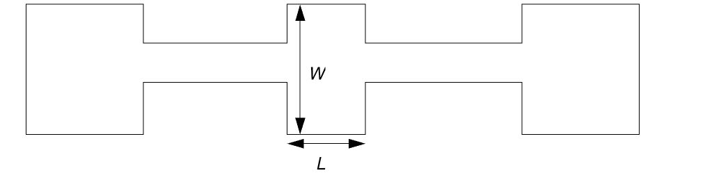
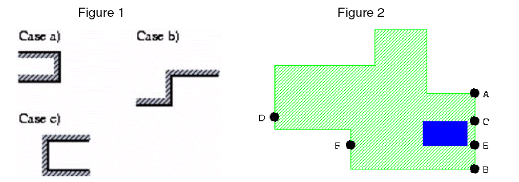
The following is a description, how the end of the metal line is identified by this option:
1.) If both angles at the ends of an edge are less than 180 degrees. In Figure 1 below, Case a is the end of a metal line (the thick black line indicates the edge of shape, thin line on the gray background indicates the direction to the inside of the shape). Case b and Case c are not.
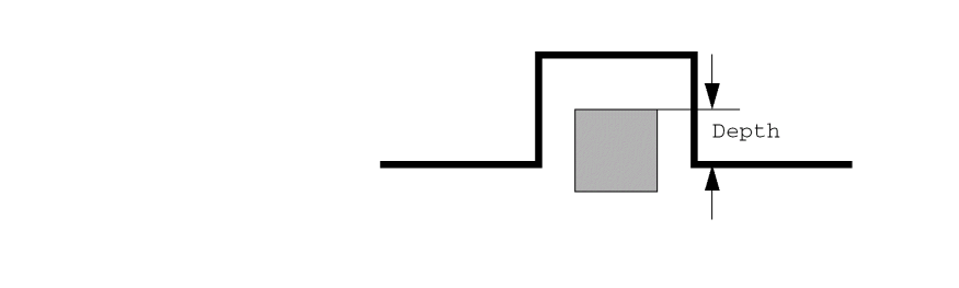
2.) The length of the edge on a metal line should be less than its length in an orthogonal direction. In Figure 2 below.the green shaded area is a metal shape, and the blue rectangle is a via. For a violation between the upper left corner of the via and point C, the length of AB is compared with the length of CD. For a violation between the lower left corner of the via and point E, the length of AB is compared with the length of EF.
Report the errors if there are at least double CORNER-EDGE errors at a corner.

If you use LT/RANGE first, CORNER-CORNER,CORNER-EDGE and CORNER-OICOR will be initialized to the specified value, then you can override them.
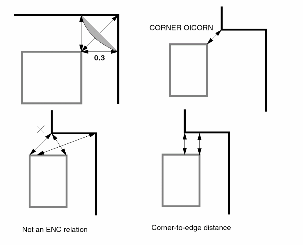
Reports the errors on the corner-to-edge distance
Reports the errors on the corner-to-corner distance. Default value is the same as CORNER-EDGE
Reports the errors on the corner-to-outside inner corner distance. Default value is the same as CORNER-EDGE. This argument only works for manhattan shapes
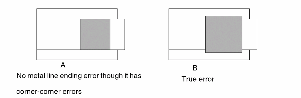
Reports errors only if the CORNER-CORNER error count of the shape is greater than or equal to the specified value (This argument only works for rectangles). In the following figure, case A will be filtered out automatically, though it has CORNER-CORNER errors.
If there is an error, reports the error only if the enclosure of the opposite side is greater than the OPPGT value. The OPPGT must be greater than the CORNER-EDGE value. It is not filtered by CERRGE.

If the via is inside the T shape, you can use the depth filter. There must be at least 2 CORNER-CORNER , 4 CORNER-EDGE, and 2 OICORN-EDGE situations. (Only works for rectangles. You must use the CERRGE option).
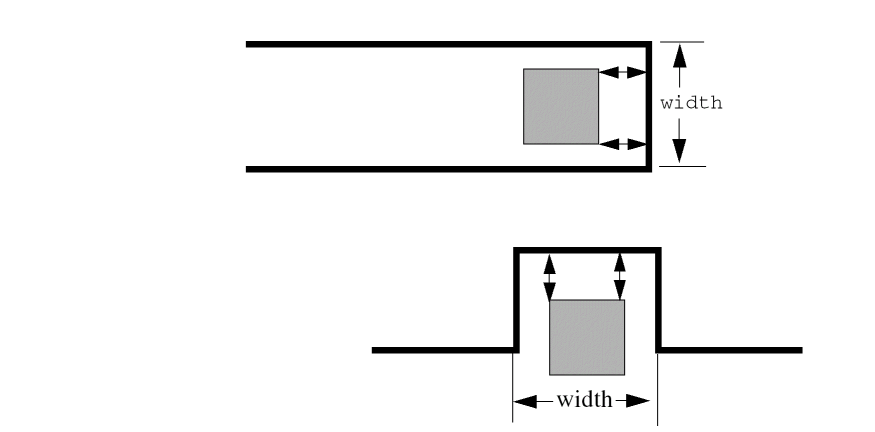
Reproduce this error only if the width is less than the specified value.
Outputs the metal line end error correction
Single and triple-corner error correction length. Default value is CORNER-CORNER/sqrt(2).
Send the results to an error cell
Example 1
DENC VIA METAL LT 0.3 OUTPUT vmerr 1
Example 2
DENC VIA METAL CORNER-EDGE LT 0.3 CORNER-CORNER LT 0.4 OUTPUT vmerr 1
Example 3
Using CERRGE to ensure there is enough metal around via
For example, X, not a real value
DENC[TOE] via metal LT 0.1 OUTPUT vmerr 1
DENC[TL] via metal LT 0.2 CORNER-CORNER LT 0.22 CERRGE 1 OUTPUT vmerr 2 sqrt(0.1**2 + 0.2**2) = 0.22
For example, Y, not a real value.
DENC[TOEL] VIA METAL LT 0.2 CERRGE 1 OUTPUT vmerr 2
DEVTAG
DEVTAGelement[type]layer-b layer-c(for tagging from a defined ELEMENT BJT device)
DEVTAG[L]  layer-a  layer-b  layer-c
(for tagging from an intermediate layer)
DEVTAG[S] BJT[type] layer-d layer-e
DEVTAG[LS] layer-c layer-f layer-g
Description
Tags multiple layers that are parts of a device with device numbers assigned by the device layer. You must define the device in the ELEMENT command before using this command. The DEVTAG command links device numbers of the layers that form multiple emitter or collector bipolar devices in the layout database.
The DEVTAG command tags device number information onto the tagged layer (layer-b) from the tagging layer (device layer or layer-a) when polygons in the tagging layer overlap or touch polygons in the tagged layer. The DEVTAG command outputs tagged polygons to output layer-c.
Multiple tagging is allowed in bipolar devices where you can link a polygon to several devices. When the tagged layer (layer-b) is not directly overlapped to the device layer, an intermediate layer (such as a SIZE layer) can tag the device number information. You do not have to tag the device layer in the ELEMENT command.
While extracting parameters from a multiple-terminal device, make sure the function or use of all generated layers from which you are extracting parameters represents the exact device (for example, MOS: gate, source-drain, and body; BJT: collector, base, emitter, and so forth). DEVTAG identifies the devices by the layer names you specify in the ELEMENT command. Thus, either the tagged layer you are extracting (layer-b) or the intermediate layers in the tagging sequence must correspond to the functional layers in the ELEMENT command.
DEVTAG[S] is used when extracting lateral PNP devices that have multi-collectors with one emitter area. Use this command to distribute the emitter area evenly to all the BJT transistors that share the same emitter in the SPICE output.
When you use the [LS] option with the DEVTAG command, it means that you are
- Tagging from an intermediate layer (layer-c), generated from the previous DEVTAG command to the tagged layer (layer-f) and putting the tagged result to the output layer (layer-g)
- Distributing the parameter values of the tagged result layer (layer-g) evenly to all the devices that share the same terminal area
The LS option is mainly used for multi-collectors with one emitter area and the emitter area is not directly overlapped to the device layer. See the section, “Example of Lateral Pnp with Possible Multiple Collector” for more information.
Arguments
Type of bipolar device used in the ELEMENT BJT[type] command. This ELEMENT[type] is the tagging device for tagging directly from the bipolar device (ELEMENT BJT). For example, BJT[NV] for a vertical npn and BJT[LP] for a lateral pnp.
Tagging (intermediate) layer. This layer must have been previously tagged with a DEVTAG (tagged from a defined ELEMENT BJT device). You must specify the L option.
Tagged layer. Contains groups of polygons, usually of the multiple collectors or emitters of a bipolar device. The specified layer carries the same device number as the tagging layer that touches or overlaps layer-b.
Output layer (intermediate layer) containing trapezoids with tagged device number information. Specify this layer for LPE only. This layer is generated from a previous tagged DEVTAG command.
Emitter layer of BJT element that you need to distribute.
Tagging intermediate layer (see layer-a for more information).
Tagged layer (see layer-b for more information).
Tagged result layer (see layer-c for more information).
Examples
In this example, the device numbers for BJT[lp] are tagged to oemit, then from oemit to emit and output to emitr. The emit1 is an intermediate layer. Through the DEVTAG command sequence, emitr can be traced back to oemit, which is the emitter layer on the ELEMENT BJT command. For more information, see Chapter 7, “Extracting Electrical Parameters (LPE).”
ELEMENT BJT[lp] coll coll base oemit
DEVTAG BJT[lp] oemit emitl
DEVTAG[L] emitl emit emitr
The following is an example of the type of lateral PNP devices. Since the collectors are used as device recognition layers, there are 4 BJT transistors defined.
PARSET BJT1 AREA PERI EA EP
ELEMENT BJT[LP] COLLPN COLLPN BASELPN EMITLPN
DEVTAG[S] BJT[LP] EMITLPN BMIT1
LEXTRACT BJT1 BMIT1 BY BJT[LP] BJTLP
C1,C2,C3,C4: COLLPN
B: BASELPN
E: EMITLPN (Area is 100u)
Example of Lateral Pnp with Possible Multiple Collector
The following is an example for extracting the distributed area & perimeter values of the shared emitter for multiple-collectors BJT device where the emitter area is not directly overlapped to the device layer. The device numbers for BJT[LP] are tagged to ovemit, then from ovemit to emit1 and output to temit.
Description
PARSET BJT1 AREA PERI EA EP CA CP
MODEL = BJT[LP], mpnp
SCHEMATIC = LVSLOGIC
....
*END
....
*OPERATION
...
ELEMENT BJT[LP] coll coll buried ovemit
...
DEVTAG BJT[LP] ovemit emit1
DEVTAG[LS] emit1 emit temit
LEXTRACT BJT1 temit BY BJT[LP] BJTLP &
LEXTRACT BJT1 coll BY BJT[LP]
LPECHK
LPESELECT[S] BJT OUTPUT spice
The SPICE netlist will look like this:
Q3 count1 in3 vcc mpnp $ CA=400 CP=80 EA=200 EP=40
Q4 count2 in3 vcc mpnp $ CA=400 CP=80 EA=200 EP=40
You can see the difference of EA and EP values between the original example (with DEVTAG[L]) and the new example (with DEVTAG[LS])
The original one’s SPICE output looks like this:
Q3 count1 in3 vcc mpnp $ CA=400 CP=80 EA=400 EP=80
Q4 count2 in3 vcc mpnp $ CA=400 CP=80 EA=400 EP=80
drcAntenna
drcAntenna information given in the 4.7 version of the Dracula Reference. Instead, use the information given below.Syntax
drcAntenna(gate( (gateLayer1 polyLayer){(gateLayer2 polyLayer)....})antenna(antLayer1{antLayer2...})diff(diffLayer1 {diffLayer2....})parset(parsetNameparameter1{parameter2...})check((antLayer1(calcparFile1 parExpr1){(calcparFile2 parExpr2)...} (chkparoptionparFile1 refLayerrel_opval1{val2} {outLayer} {(outputc-name l-num{data-type})}) {(chkparoption parFile2 ...) ...} ) {(antLayer2parFile3 parExpr3)...} ) )
Description
Simplifies the way you write antenna check rules.
The antenna checking summary is written into a printfile.sum file. The printfile is defined in the DESCRIPTION block by PRINTFILE.
drcAntenna assumes that all metal layers connected to the diffusion layer are considered as safe and that the top metal layer connected to the I/O pads will be ignored due to the protection circuit.
drcAntenna supports the cumulated charging methods. The gates not connected to the diffusion layer, but having the same nodal information will be calculated separately because the charging effect might be underestimated if calculated together.
Users do not need to distinguish the type of gates because it makes no difference during antenna checking.
drcAntenna supports poly and contact checks in the 4.8 version. See Example 4 and Example 5 in the following pages for details.
Arguments
The initial value for chkpar. The keyword introducing the layers to be measured for the gate area of the check. It has the following form:
gate( (gateLayer1 polyLayer) {(gateLayer2 polyLayer)...})
where gateLayer1 is derived from polyLayer, and gateLayer2 is derived from polyLayer, and so on. Although it is not required, it is better to specify a single gateLayer because if more than one gateLayer is specified, the layers are automatically merged into one internal gateLayer.
Keyword introducing the routing layers to be measured for the antenna area of the check. It has the following form:
antenna(antLayer1{antLayer2...}),
where antLayer1, antLayer2, and so on are routing layers.
Keyword introducing the diffusion source/drain layers. If any shape in the routing layers is connected to the given diffusion layers, the nets of the shapes are assumed to be connected to diodes and excluded from calculating the antenna area. This argument has the following form:
diff(diffLayer1 {diffLayer2 ...})
Although it is not required, it is better to use a single diffLayer layer, because if more than one diffLayer layer are specified, the layers are automatically merged into one internal diffLayer.
CONNECT or SCONNECT commands in the OPERATION block.This keyword introducing the parameter set to be used for Dracula to record data. It has the following form:
parset( parsetNameparm1{parm2...} )
Keyword that defines the antenna check to be performed after a particular layer is processed. It has the following form:
check( (antLayer1(calcparFile1 parExpr1)
{(calcparFile2 parExpr2).... )}
(chkparoptionparFile1 refLayerrel_opval1{val2} {outLayer1}
(outputc-name l-num{data-type})} ...)
(chkparoptionparFile2 refLayerrel_opval1 {val2}{outLayer2}
{(outputc-name l-num{data-type})} ...)} )
(antLayer2(calcparFile3 parExpr3)
{(calcparFile4 parExpr4).... }
(chkparoptionparFile3 refLayerrel_opval1 {val2}
{outLayer3}
{(outputc-name l-num{data-type})} ... )
(chkparoptionparFile4 refLayerrel_opval1{val2}
{outLayer4}
{(outputc-name l-num{data-type})} ...)} )
)
The calc command specifies what kinds of parameter to be derived from the nodes among multiple layers. The parExpr in the calc command could be expressed in terms of the previous parameters derived from a particular antLayer, which means a cumulated model will be used for calculating that parameter.
The chkpar command specifies the conditions to be checked on the parameters calculated from the calc command. You can supply an optional output field to direct the violated shapes from the refLayer to a particular error cell. You can specify one of the following options in the check command.
drcAntenna command, for every antenna layer that you have specified in the drcAntenna syntax, you must also use them in the check sub-function. PDRACULA will not check for completeness of the layers specified in the check sub-function. drcAntenna( gate( GATE POLY ) antenna( M1 M2 M3 M4 ) diff( PSD ) parset( ANTP AREA ) check( ( M4 ( calc PARM4=M4.AREA/GATE.AREA )
( chkpar par PARM4 GATE gt 3 ERR4 output ERR4 1))
Although PDRACULA will not report any syntax error when it compiles, your Dracula job will not complete and will get aborted because only the M4 antenna layer was specified in the check sub-function. The M1, M2, and M3 layers were not included.
Check the computed AREA ratio as stored in the parFile.
Check the computed AREA value or ratio as stored in the parFile.
Check the computed perimeter value or ratio as stored in the parFile.
The antenna parameters are calculated right after the antLayer is calculated. These calculations are followed by a chkpar on the parFile subject to the specified condition.
Diode Area Checking with drcAntenna
If there is layer name DIODE in the following lines, you can calculate diode ratios at any check level:
DIFF (DIODE)
ANTENNA (antLayer1 {antLayer2 ...} DIODE)
In this case you can write an expression in the rule such as (calc parFile1 parExpr1). For example:
(calc parFile2_DIODE parExpr2_DIODE)
Where, parExpr2_DIODE is an expression dependent on DIODE layer parameter (such as DIODE.AREA or DIODE.PERI), for example:
(CALC RD1A = DIODE.AREA)
(CALC RD1P = DIODE. PERI)
(CALC RM1A = ME1.AREA/GATE.AREA)
To check antenna ratios for connected and unconnected to diode layers with ratio of corresponding diode value you must write:
(chkpar option parFile1 refLayer rel_op1 val1 with parFile2_DIODE rel_op2 val2 {(output c-name l-num {data-type})})
Where, rel_op2 can be LT; LE or for val2=0 rel_op2 is EQ. For example:
(CHKPAR RM1A GATE GT 400 with RD1A LT 0.036 ERMD1A OUTPUT EMD1A 45 )
This rule means that the layer ERMD1A contains gate layer shapes which are connected to metal1 with an area ratio greater than 400 and this metal1 is either connected to diode with an area less than 0.036 or not connected to any diode (diode area equals nil).
The DIODE must be the latest layer name for ANTENNA and it must be used a single diffLayer (DIODE) in this case (see the Arguments for this command). If there is no layer name of DIODE, then ANTENNA runs without the diode check using the prior rule syntaxes without the “with” option:
ANTENNA (antLayer1 {antLayer2 ...})
Examples
For antenna checking, form the correct connectivity.
Attached is a four-metal technology file which contains all the information required for an antenna check. First, you calculate PARME1, partial antenna ratio (PAR) for ME1 after the placement of ME1 layer. At that time, ME2, ME3 and ME4 are not deposited. Next, you find PARME2, PAR for ME2, and PARME3, PAR for ME3, respectively. Finally, after all layers are deposited, you sum up the antenna ratio from PARME1, PARME2 and PARME3, which is the sum of the PARs of all nodes connected on top of nodes from the refLayer, GATE. You use the default(sum) mode for choosing the gate area in antenna ratio calculation. You don’t need to extract ME4, because there is an I/O pad with the protection circuit.
Example 1
*DESCRIPTION
 ...
*END
*INPUT-LAYER
 DIFF = DIFF
 POLY = POLY
 CONT = CONTACT
 ME1  = MET1
 ME2  = MET2
 ME3  = MET3
 ME4  = MET4
 VA1  = VI1
 VA2  = VI2
 VA3  = VI3
;CONNECT LAYERS SEQUENCE
 CONNECT-LAYER = SDL POLY ME1 ME2 ME3 ME4
*END
*OPERATION
;LAYERS DERIVATION
;
 ANDNOT   DIFF   POLY    GATE    SDL
;
;********* CONNECT STATEMENTS  ********
;
 CONNECT  ME4    ME3     BY      VA3
 CONNECT  ME3    ME2     BY      VA2
 CONNECT  ME2    ME1     BY      VA1
 CONNECT  ME1    POLY    BY      CONT
...
;
;ANTENNA PARAMETERS EXTRACTION
;
drcAntenna(
   gate( GATE POLY )
   antenna( ME1 ME2 ME3 )
   diff( SDL )
   parset( ANTP AREA )
   check(( ME1 (calc PARME1= ME1.AREA / GATE.AREA)
               (chkpar par PARME1 GATE GT 100 errme1 output ERR 1))
         ( ME2 (calc PARME2= ME2.AREA / GATE.AREA)
               (chkpar par PARME2 GATE GT 100 errme2 output ERR 2))
         ( ME3 (calc PARME3= ME3.AREA / GATE.AREA)
               (calc CARME=PARM1+PARM2+PARM3)
               (chkpar par PARME3 GATE GT 100 errme2 output ERR 3)
               (chkpar par CARME  GATE GT 100 errmet output ERR 4))
        )
   )
*END
Example 2
This example uses the traditional method to do antenna checking.
*DESCRIPTION
...
*END
*INPUT-LAYER
 NDIFF = NDIFF
 PDIFF = PDIFF
 POLY  = POLY
 CONT  = CONTACT
 ME1   = MET1
 ME2   = MET2
 ME3   = MET3
 VA1   = VIA1
 VA2   = VIA2
;CONNECT LAYERS SEQUENCE
 CONNECT-LAYER = SDL NSD PSD POLY ME1 ME2 ME3
*END
*OPERATION
;LAYERS DERIVATION
 ANDNOT   NDIFF   POLY    NGATE   NSD
 ANDNOT   PDIFF   POLY    PGATE   PSD
 OR       NSD     PSD     SDL
 OR       PGATE   NGATE   GATE
;
;********* CONNECT STATEMENTS  ********
;
 CONNECT  ME3    ME2      BY      VA2
 CONNECT  ME2    ME1      BY      VA1
 CONNECT  ME1    POLY     BY      CONT
 CONNECT  ME1    PSD      BY      CONT
 CONNECT  ME1    NSD      BY      CONT
 CONNECT  ME1    SDL      BY      CONT
 ...
;
;ANTENNA PARAMETERS EXTRACTION
;
drcAntenna(
   gate( GATE POLY )
   antenna( ME1 ME2 ME3 )
   diff( SDL )
   parset( ANTP AREA )
   check(( ME1 (calc PARME1= ME1.AREA/GATE.AREA)
               (chkpar par PARME1 GATE GT 100 errme1 output ERR 1))
         ( ME2 (calc PARME2=(ME1.AREA+ME2.AREA)/GATE.AREA)
               (chkpar par PARME2 GATE GT 100 errme2 output ERR 2))
         ( ME3 (calc PARME3=(ME1.AREA+ME2.AREA+ME3.AREA)/GATE.AREA)
               (chkpar par PARME3 GATE GT 100 errme2 output ERR 3))
        )
   )
;
*END
Example 3
*DESCRIPTION
...
*END
*INPUT-LAYER
 NPLUS = NPLUS
 PPLUS = PPLUS
 POLY  = POLY
 CONT  = CONTACT
 MT1   = MET1
 MT2   = MET2
 MT3   = MET3
 VA1   = VIA1
 VA2   = VIA2
;CONNECT LAYERS SEQUENCE
 CONNECT-LAYER = SDL NSD PSD POLY MT1 MT2 MT3
*END
*OPERATION
;LAYERS DERIVATION
 ANDNOT   NPLUS   POLY   NGATE   NSD
 ANDNOT   PPLUS   POLY   PGATE   PSD
 OR       NSD     PSD    SDL
 OR       PGATE   NGATE  GATE
;
;********* CONNECT STATEMENTS  ********
;
 CONNECT  MT3     MT2    BY     VA2
 CONNECT  MT2     MT1    BY     VA1
 CONNECT  MT1     POLY   BY     CONT
 CONNECT  MT1     PSD    BY     CONT
 CONNECT  MT1     NSD    BY     CONT
 CONNECT  MT1     SDL    BY     CONT
;
;ANTENNA PARAMETERS EXTRACTION
;
drcAntenna(
     gate( GATE POLY )
     antenna( MT1 MT2 MT3 )
     diff( SDL )
     parset( ANTP AREA )
     check(( MT1 (calc PARM1 = MT1.AREA/MIN.GATE.AREA )
             (chkpar par PARM1 GATE  GT 100 EX1)
             (chkpar par PARM1 MT1   GT 100 EX2))
           ( MT2 (calc PARM2 = (MT1.AREA+MT2.AREA)/MIN.GATE.AREA)
             (chkpar par PARM2 GATE  GT 100 EX3)
             (chkpar par PARM2 MT2   GT 100 EX4))
           ( MT3 (calc PARM3 = (MT1.AREA+MT2.AREA+MT3.AREA)/MIN.GATE.AREA)
              (chkpar par PARM3 GATE GT 100 EX5)
              (chkpar par PARM3 MT3  GT 100 EX6))
          )
   )
;
    OR  EX1  EX3  ERR1
    OR  ERR1 EX5  ERRGATE

*END
Example 4
drcAntenna allows users to do the poly layer antenna check.
drcAntenna(
    gate(GATE POLY)
    antenna(POLY MET1 MET2)
    diff(DIFF)
    parset(ANTP AREA PERI)
    check(
       (POLY (calc    PARM0 = POLY.AREA/GATE.AREA)
             (chkpar  PARM0 RA 0  500 OUTPUT ER0 01))
       (MET1 (calc    PARM1 = MET1.AREA/GATE.AREA)
    (chkpar  PARM1 RA 0  500 OUTPUT ER1 01))
       (MET2 (calc PARM2 = MET2.AREA/GATE.AREA)
             (calc SUM = PARM0+PARM1+PARM2)
    (chkpar  PARM2 RA 0  500 OUTPUT ER2 01)
             (chkpar SUM RA 0 500 OUTPUT ER3 01))
))
The reflayer is not specified in chkpar, for example,
chlpar PARM1 RA 0 500 OUTPUT ER1 01 will be considered as:
chlpar PARM1 GATE RA 0 500 OUTPUT ER1 01 &
chlpar PARM1 POLY RA 0 500 OUTPUT ER1 02 &
chlpar PARM1 MET1 RA 0 500 OUTPUT ER1 03 &
Example 5
drcAntenna allows you to do a contact layer antenna check, but it should not be specified in the antenna layer. Here is an example for it.
drcAntenna(
    gate(GATE POLY)
    antenna(MET1 MET2)
    diff(DIFF)
    parset(ANTP AREA PERI)
    check((MET1 (calc    PARM1 = MET1.AREA/GATE.AREA)
             (chkpar  PARM1 RA 0  500 OUTPUT ER1 01)
    (calc    PARM2 = CONT.AREA/GATE.AREA)
             (chkpar  PARM2 RA 0  500 OUTPUT ER2 01))
    (MET2 (calc    PARM3 = MET2.AREA/GATE.AREA)
             (chkpar  PARM3 RA 0  500 OUTPUT ER3 01)
    (calc    PARM4 = VAI.AREA/GATE.AREA)
             (chkpar  PARM4 RA 0  500 OUTPUT ER4 01)
             (calc CARM1 = PARM1+PARM2+PARM3+PARM4)
             (chkpar CARM1 RA 0 500 output ER5 01))
     )
Example 6
Diode Area Checking with drcAntenna
*DESCRIPTION
MAG-BEF-GRID=YES
INDISK=antenna_0409_3.gds
PRIMARY=ANTENNA1
OUTDISK=test1.out
PRINTFILE=test1
MODE=EXEC NOW
SYSTEM=GDS2
SCALE=0.001 MICRON
RESOLUTION=0.001 MICRON
LISTERROR=YES
KEEPDATA=YES
FLAG-NON45=YES
FLAG-OFFGRID=YES 0.001
FLAG-ACUTEANGLE=YES
FLAG-SELFINTERS=YES
CNAMES-CSEN=YES
*END
*INPUT-LAYER
SUBSTRATE=PSUB 0
NWEL=3
DIFF=1
PO1=41
NPLUS=12
PPLUS=11
SAB=36
CONT=39
ME1=46
VI1=47
ME2=48
VI2=49
ME3=50
VI3=51
ME4=52
VI4=53
ME5=54
VI5=55
ME6=56
PAD=66
CONNECT-LAYER = DIODE PSD NSD PO1 ME1 ME2 ME3 ME4 ME5 ME6
*END
*OPERATION
SEL DIFF OVERLAP NWEL DIFNW
NOT DIFF DIFNW DIFPS

NOT DIFPS PPLUS NDIF
AND DIFNW PPLUS PDIF

AND PO1  DIFF GATE
NOT PDIF PO1 PSD
NOT NDIF PO1 NSD
OR  PSD  NSD DIODE

CONNECT ME6 ME5 BY VI5
CONNECT ME5 ME4 BY VI4
CONNECT ME4 ME3 BY VI3
CONNECT ME3 ME2 BY VI2
CONNECT ME2 ME1 BY VI1
CONNECT ME1 PO1 BY CONT
CONNECT ME1 PSD BY CONT
CONNECT ME1 NSD BY CONT
CONNECT ME1 DIODE BY CONT
drcAntenna(
GATE( GATE PO1 )
DIFF( DIODE )
ANTENNA( PO1 ME1 ME2 ME3 ME4 ME5 ME6 DIODE )
PARSET( ANT0 AREA PERI )
CHECK(
( PO1 ( CALC RP1A = PO1.AREA/GATE.AREA )
( CALC RDP1A = DIODE.AREA )
( CHKPAR RP1A GATE GT 100 with RDP1A LT 0.005 OUTPUT EP1A 45 ))
( ME1 ( CALC RM1A = ME1.AREA/GATE.AREA )
( CALC RM1CA = RP1A+RM1A )
( CALC RDM1A = DIODE.AREA )
       ( CHKPAR RM1A GATE GT 400 with RDM1A LT 0.005 ERM1A OUTPUT EM1A 45 )
       ( CHKPAR RM1CA GATE GT 400 with RDM1A LT 0.005 ERM1CA OUTPUT EM1CA 45 ))
( ME2 ( CALC RM2A = ME2.AREA/GATE.AREA )
( CALC RM2CA = RP1A+RM1A+RM2A )
( CALC RDM2A = DIODE.AREA )
       ( CHKPAR RM2A GATE GT 400 with RDM2A LT 0.005 ERM2A OUTPUT EM2A 45 )
       ( CHKPAR RM2CA GATE GT 400 with RDM2A LT 0.005 ERM2CA OUTPUT EM2CA 45 ))
( ME3 ( CALC RM3A = ME3.AREA/GATE.AREA )
( CALC RM3CA = RP1A+RM1A+RM2A+RM3A )
( CALC RDM3A = DIODE.AREA )
       ( CHKPAR RM3A GATE GT 400 with RDM3A LT 0.005 ERM3A OUTPUT EM3A 45 )
       ( CHKPAR RM3CA GATE GT 400 with RDM3A LT 0.000 ERM3CA OUTPUT EM3CA 45 ))
( ME4 ( CALC RM4A = ME4.AREA/GATE.AREA )
( CALC RM4CA = RP1A+RM1A+RM2A+RM3A+RM4A )
( CALC RDM4A = DIODE.AREA )
       ( CHKPAR RM4A GATE GT 400 with RDM4A LT 0.005 ERM4A OUTPUT EM4A 45 )
       ( CHKPAR RM4CA GATE GT 400 with RDM4A LT 0.005 ERM4CA OUTPUT EM4CA 45 ))
( ME5 ( CALC RM5A = ME5.AREA/GATE.AREA )
( CALC RM5CA = RP1A+RM1A+RM2A+RM3A+RM4A+RM5A )
( CALC RDM5A = DIODE.AREA )
       ( CHKPAR RM5A GATE GT 400 with RDM5A LT 0.005 ERM5A OUTPUT EM5A 45 )
       ( CHKPAR RM5CA GATE GT 400 with RDM5A LT 0.005 ERM5CA OUTPUT EM5CA 45 ))
( ME6 ( CALC RM6A = ME6.AREA/GATE.AREA )
( CALC RM6CA = RP1A+RM1A+RM2A+RM3A+RM4A+RM5A+RM6A )
( CALC RDM6A = DIODE.AREA )
    ( CHKPAR RM6A GATE GT 400 with RDM6A LT 0.005 ERM6A OUTPUT EM6A 45 )
    ( CHKPAR RM6CA GATE GT 400 with RDM6A LT 0.005 ERM6CA OUTPUT EM6CA 45 ))
))
*END
ECONNECT
ECONNECTelem{[type]}layerCONN/DISClabel{trapfile} OUTPUTc-name l-num{d-num} {&}
Description
Outputs elements that are connected (or disconnected) from a labeled node through a specified layer.
Arguments
Type of element being checked. You must define this element using the ELEMENT command.
MOS = MOS devices PAD = PAD windows LDD = LDD devices
Two-letter (A-Z) code that denotes the type of MOS device. Used to differentiate N-channel from P-channel in CMOS or to differentiate MOS devices with different implants.
Layer through which connections are being checked. A layer name of ALL checks all elem and type conductor layers defined in the ELEMENT command.
CONN means a connection to the labeled node is a violation.
DISC means a disconnection from the labeled node is a violation.
Text label of the node considered for the check. The label must have text assigned in the layout database and conform to the text rules.
Name of the output file to contain composite trapezoids. Before you perform any subsequent operation on a trapfile, you need to “OR” it with itself or with the substrate. This merges the multiple layers.
Sends the results of the operation to an output cell.
C-name is the name of the output cell and can have six alphanumeric characters or fewer and no special characters. L-num is the cell layer number determined by your CAD system. If your c-name is rule03 and l-num is 5, the output cell name is rule0305.
The datatype number associated with the layer number (l-num) of the output cell. Use d-num for GDSII only. Values can range from 0 to 63.
The ampersand indicates a conjunctive rule. This command can be joined to other ECONNECT and NDCOUNT commands.
Elements that satisfy the ECONNECT command are collected in an output cell. This data in the output cell is the device layer of the element. For silicon-gate MOS, this is the channel region layer.
Examples
The following example checks all MOS P-type elements connected to VSS (the labeled node) through the predefined srcdrn layer. The elements that satisfy the condition are output as cell name cell110 on layer 10.
ECONNECT MOS[P] srcdrn CONN vss OUTPUT cell1 10
The following example collects all MOS elements connected to VCC through srcdrn. The result is passed on to a second check. The elements that satisfy this condition are connected to VSS through srcdrn. Thus, output cell211 on layer 11 has all transistors connected to power and ground simultaneously through the source/drain layers.
ECONNECT MOS srcdrn CONN vcc &
ECONNECT MOS srcdrn CONN vss OUTPUT cell2 11
The following example collects all BJT[N] elements connected to VCC through the coll (collector). The result is passed on to a second check. The elements that satisfy this condition are connected to GND through emit (emitter). Thus, the output cell dever115 on layer 15 has all transistors connected to power and ground simultaneously.
ECONNECT BJT[N] coll CONN vcc &
ECONNECT BJT[N] emit CONN gnd OUTPUT dever1 15
EDGECHK
EDGECHK layer {ANGLE[90/-90]} LENGTH GT value1 {trapfile} {OUTPUT ERR layerno {datatype}}
Description
This command checks the length of 45 non-manhattan edge in GATE.
Arguments
Manhattan edge (parallel with X-Y axis)
Allowed operations are LT,RA,GT
By default, the output edge is inside the shape. If you use [O], the edge is outside the shape.
Example
EDGECHK gate ANGLE[-90] LENGTH GT 1.0 OUTPUT ERR 01
EDTEXT
EDTEXT = text-coordinate-file
Description
Specifies to use text from a text coordinate file in addition to text in the design. The text coordinate file is a free-format, 80-column text file. Each line specifies one text label, its x,y coordinates, and, optionally, its attached layer name. The x,y coordinates contain significant digits equivalent to the resolution.
Significant digits is the number of digits behind the decimal point. For example, if you set the resolution to .01, the x,y coordinate should have two digits after the decimal point (such as, .33). If the resolution is .001, the x,y coordinate should have three digits after the decimal point (for example, .333).
Text labels not located at two significant digits are rounded up and possibly discarded if they conflict with other text labels at the same coordinate.
The text coordinate file can contain spaces, empty lines, tab characters, or comments (;). The comment must be on its own line. You can put the comment starter (;) in the first column of a line, or you can precede it with blank spaces. You cannot put a comment at the end of a line of text in an EDTEXT file. Dracula ignores all text after the comment starter. The following is an example of a valid file:
ABC:I   X=   10  Y= -200
VCC     X=  120  Y=   40  Attach=Metal
VSS     X= -120  Y=  -40
IN      X=  -10  Y=  -10
OUT     X=  0.5  Y=   40
If you specify a layer name for attaching the text, the text is attached to that layer only. If you do not specify a layer name, the text is attached to one of the layers according to the TEXTSEQUENCE or CONNECT-LAYERS commands.
When both the CAD graphics system database and the text coordinate file have different texts at the same location, the CAD system text is discarded. You can override or delete the graphics system text. To delete the graphics system text, specify an illegal text (for example, 99) in the EDTEXT file with the same coordinates as the graphics system text.
Place the EDTEXT command above the CONNECT command in the Operation block.
Example
*OPERATION
.
EDTEXT = ram.txt
.
.
CONNECT metal poly BY cont
.
.
*END
ELCOUNT
ELCOUNTelem{[type]}layer condition n1{trapfile} OUTPUTc-name l-num{d-num} {&}
Description
Counts the number of elements connected through specific layers in a node. The command outputs the nodes with specified element counts to an output cell.
Arguments
Type of element being checked. You must define this element using the ELEMENT command.
MOS = MOS devices BJT = Bipolar devices PAD = PAD windows LDD = LDD devices
Two-letter (A-Z) code that denotes the type of device. This can differentiate N-channel from P-channel in CMOS or differentiate MOS devices with different implants.
Layer through which the connections are being checked. A layer name of ALL checks all elem and type conductor layers defined in the ELEMENT command.
The tests according to one of the following conditions:
where the number (n1) can be an integer between 0 and 63.
Name of the output file to contain composite trapezoids. Before you perform any subsequent operation on a trapfile, you need to “OR” it with itself or with the substrate. This merges the multiple layers.
Sends the results of the operation to an output cell. The output cell you specify cannot be used as the output of another command.
C-name is the name of the output cell and can have six alphanumeric characters or fewer and no special characters. L-num is the cell layer number determined by your CAD system. If your c-name is rule03 and l-num is 5, the output cell name is rule0305.
Datatype number associated with the layer number (l-num) of the output cell. Use d-num for GDSII only. Values can range from 0 to 63.
Indicates a conjunctive rule. This command can be joined to other ELCOUNT and PROBE commands.
Examples
This example detects all floating nodes that have no connection with the element through the srcdrn layer. The output cell name is float60.
ELCOUNT MOS srcdrn EQ 0 OUTPUT float 60
This example detects nodes that are connected to only one MOS element. The output cell name is single60.
ELCOUNT MOS all EQ 1 OUTPUT single 60
In the following example, the first command collects nodes that are connected to more than 60 elements through the srcdrn layer. The second command checks the nodes further to see if they are connected to predefined pads. The output cell name is bignod40.
ELCOUNT MOS srcdrn GT 60 &
ELCOUNT PAD metal EQ 0 OUTPUT bignod 40
The following example detects nodes that are connected to only one bipolar element. The output cell name is onedev20.
ELCOUNT BJT all EQ 1 OUTPUT onedev 20
ELEMENT BJT
ELEMENT BJT{[type]} layer-a layer-b layer-c layer-d {layer-s}
Description
Arguments
Two-character code that denotes the type of BJT device. The first character must be any letter from A-Z. The second character is optional and can be any letter from A-Z or any number from 0-9 (except for 8). You can use this code to differentiate BJT devices. For example, vertical npn devices are type NV and lateral pnp devices are type PL.
Device layer, one region per device. This layer defines the device region that touches or overlaps the bipolar conductor layers. For an npn device, this is usually defined by the emitter. For a lateral pnp device, this is usually defined by the collector.
Terminal conductor layer for the collector terminal. This layer must carry node information.
Terminal conductor layer for the base terminal. This layer must carry node information.
Terminal conductor layer for the emitter terminal. This layer must carry node information.
Substrate terminal layer. If you define this substrate layer, LVS checks for discrepancies or inconsistencies found in the layout or schematic. Discrepancies are reported in the LVS report file. You must also add a CDL definition for substrate.
Note:- ELEMENT BJT should not have terminal layer names with the 3 first letters BJT.
-
In general, the device layer used for a vertical npn device must be the emitter region because an npn can have multiple emitters. Also, the emitter region overlaps all three terminals of this device. For the lateral pnp, the device layer must be the collector region because a pnp can have multiple collectors. The collector layer does not touch or overlap the emitter layer for its terminal connection. To overcome this, the emitter layer is oversized to overlap the collector device layer and then stamped with node information.
Examples
In the following example, the enpn is the emitter region and device layer. Layers buried, base, and nplus are the BJT terminal conductors and they must carry node information.
ELEMENT BJT[NV] enpn buried base nplus
In this example, cpnp1 is the collector region and device layer.
ELEMENT BJT[PL] cpnp1 base buried oepnpl
This example shows the ELEMENT command with a substrate layer defined. The name specified here is WELL, but you can specify any name.
ELEMENT BJT[A] BJTW COLL BASE EMIT WELL
For additional discussion and illustrations of bipolar devices, refer to Chapter 7, “Extracting Electrical Parameters (LPE).”
ELEMENT BOX
ELEMENTdevicelayer-a layer-b{layer-c} {layer-d} {layer-e}
Description
Defines devices with a variable number of terminals. This command lets you define special devices (that is, element types other than BJT, CAP, DIO, LDD, MOS, PAD, or RES).
Arguments
Three-character name that denotes a user-defined device. The name can have only characters A-Z. However, the first character cannot be B, C, D, L, M, P, or R. This name must match the name of an empty .SUBCKT in the netlist corresponding to the ELEMENT BOX.
Device layer, one region per device, that touches or overlaps the device conductor layers.
Position No. 1 terminal conductor layer with zero to multiple nodes. This is the conductor layer for the position No. 1 terminal and must carry node information.
Position No. 2 terminal conductor layer with zero to multiple nodes. This is the conductor layer for the position No. 2 terminal and must carry node information.
Position No. 3 terminal conductor layer with zero to multiple nodes. This is the conductor layer for the position No. 3 terminal and must carry node information.
Position No. 4 terminal conductor layer with zero to multiple nodes. This is the conductor layer for the position No. 4 terminal and must carry node information.
Note:Example
This example is for a p+ diffusion resistor element with a buried layer underneath the resistor.
ELEMENT ISP pdifres cont buried
ELEMENT CAP
ELEMENT CAP {[type]} layer-a layer-b layer-c {layer-s}
Description
Defines a capacitor device. This command does not define an LPE parasitic element. See also the PARAMETER CAP section in this chapter.
Arguments
Two-character code that denotes the type of CAP device. The first character must be a letter from A-Z. A second character is optional and can be any letter from A-Z or a number from 0-9 (except 8). This code differentiates capacitor devices.
Device layer, one region per device, that defines the capacitor region that touches or overlaps the capacitor conductor layers.
Terminal conductor layer for one side of the capacitor. This layer must carry node information.
Terminal conductor layer for the other side of the capacitor. This layer must carry node information.
Substrate terminal layer. If you define this substrate layer, LVS checks for discrepancies or inconsistencies found in the layout or schematic. Discrepancies are reported in the LVS report file. You must also add a CDL definition for substrate.
Note:Example 1
*INPUT-LAYER
.
.
CONNECT-LAYER=pwell nsd psd pl1 pl2 metal
*END
*OPERATION
AND pl1 pl2 p12cap    ; poly1 to poly 2 capacitor
CONNECT pl1 pl2 BY cont2
CONNECT metal pl2 BY cont1
CONNECT metal pl1 BY cont1
.
.
ELEMENT CAP[PP] p12cap pl2 pl1
ELEMENT CAP[A] metpwel metal pwell
You can check ELEMENT CAP polarity in LVS or LPE when you specify the P option in LVSCHK or LPECHK. When you specify the P option, you cannot swap layer-b and layer-c.
You can also check the ELEMENT CAP type in LVS or LPE when you specify LVSCHK or LPECHK. The schematic CDL netlist must specify the type for the capacitors to check. For more information, refer to Chapter 5, "Compiling Network Descriptions (LOGLVS)."
Example 2
*OPERATION
.
.
ELEMENT CAP[PP] p12cap pl2 pl1
ELEMENT CAP[A] metpwel metal pwell
.
.
LVSCHK[P]
*END
C1 sig1 sig2 3pf $ [PP] or $.MODEL=PP
C2 sig3 sig4 1 pf $ [A] or $.MODEL=A
ELEMENT DIO
ELEMENT DIO {[type]} layer-a layer-b layer-c {layer-s}
Description
Defines the P-N junction diode. This command does not define an LPE element.
Arguments
Two-character code that denotes the type of DIO device. The first character must be a letter from A-Z. The second character is optional and can be any letter from A-Z or any number from 0-9 (except 8). This code differentiates diode devices. For example, P-diode to N-substrate devices are [P] type, and N-diode to P-well devices are [N] type.
Device layer, one region per device. This layer defines the diode region that touches or overlaps the anode and cathode conductor layers.
Anode conductor layer for the anode terminal, usually the p+ diffusion or the P-well. This layer must carry node information.
Cathode conductor layer for the cathode terminal, usually the n+ diffusion or the N-substrate. This layer must carry node information.
Substrate terminal layer. If you define this substrate layer, LVS checks for discrepancies or inconsistencies found in the layout or schematic. It reports discrepancies in the LVS report file. You must also add a CDL definition for substrate.
Note:Example
*INPUT-LAYER
.
CONNECT-LAYER=nsub pwell nsd psd poly metal
*END
*OPERATION
.
AND psd diode pdio    ; identify the P+ pdio
CONNECT metal nsd BY cont
CONNECT metal psd BY cont
CONNECT nsd nsub BY ntnsub
.
ELEMENT DIO[P] pdio psd nsub
;For a p+ diode element to the n-substrate.
ELEMENT IN?
ELEMENT device layer-a layer-b layer-c {layer-s}
The above is the ELEMENT IN? syntax in the “Operation Block of Commands” of your rule file when the PARSET command’s syntax in the “Description Block of Commands” of your rule file is as follows:
PARSET = pname param1 param2 param3,...paramn
The ? in the ELEMENT IN? command stands for any alphabet, but the first 2 characters of the device name definitely need to start with IN.
Description
Allows you to use BOX devices to simulate inductors and extract some important parameters for the inductors, such as the number of turns, diameter of inner circle, etc. and output them to the SPICE netlist file for supporting inductors in layout designs.
The first step is to use PARSET command to specify what parameters will be extracted. There are four geometric primitives regarding inductors provided: ID, IN, IW, and IS and one reserved parameter, LL. See the PARSET command in “Description Block Commands” chapter of this manual for more information on these four primitives and reserved parameter. See the “Supporting Inductors in Layout Designs Using the PARSET and ELEMENT IN? Commands” section in the “Extracting Electrical Parameters (LPE)” chapter of this manual for information on the different types of inductors.
Arguments
User-defined device name with three characters. The first two characters should be IN.
Device layer, one region per device.
Terminal layer for one side of the inductor.
Terminal layer for the other side of the inductor.
Example
PARSET = TEST ID IN IW IS LL
ELEMENT IND INDSYM ME4 ME5
LEXTRACT TEST INDSYM BY IND INDPAR1 &
EQUATION LL=ID+IN+IW+IS
LPESELECT[NY] IND output SPICE
ELEMENT LDD
ELEMENT LDD {[type]} layer-a layer-b layer-c layer-d
{layer-e}
Description
Defines a MOS element whose source and drain cannot be swapped.
Arguments
Two-character code used to denote the type of LDD (lightly doped drain MOS) device. The first character must be a letter from A-Z. The second is optional and can be any letter from A-Z or any number from 0-9 (except 8). This code differentiates MOS devices with different implants. For example, CMOS pull-up devices are P type and pull-down devices are N type. NMOS devices are E, D, and N types. See the following note about the special LDD[X-] type.
Device layer, one region per device. This layer defines the device region that touches or overlaps the device conductor layers. For silicon-gate MOS, this is the channel region layer usually defined by the overlapped area of polysilicon and diffusion. For a gallium arsenic transistor, this is the channel region layer usually defined by the overlapped area of schottky metal and lightly doped diffusion. For metal-gate MOS, this is the gate region usually defined by the thin oxide mask.
Gate conductor layer. For silicon-gate MOS, this is the polysilicon layer. For metal-gate MOS, this is the metal layer; for gallium arsenic, this is the schottky metal layer. This layer must carry node information.
Lightly doped drain conductor layer. For silicon-gate MOS, this is the self-aligned lightly doped diffusion layer, usually defined by the lightly doped diffusion layer excluding the channel regions. For metal-gate MOS, this is the lightly doped diffusion layer. This layer must carry node information.
Source conductor layer. For silicon-gate MOS, this is the self-aligned diffusion layer, usually defined by the diffusion layer excluding the channel regions. For metal-gate MOS, this is the diffusion layer. This layer must carry node information.
Substrate conductor layer. This substrate layer is for optional use in running LVS or LPE checking substrate connection mismatch. For MOS: usually N-well, P-well, N-substrate, or P-substrate. If you specify this layer, it must carry node information.
Note:- ELEMENT LDD should not have terminal layer names with the 3 first letters LDD.
-
A special LDD[X-] type stops the generation of pseudo gates when you run an LVS check. To disallow devices from forming pseudo gates, specify an ELEMENT LDD command where the first character type is an X and the second character type is either a letter from A-Z or a number from 0-9 (except 8). This allows LVS to locally stop the formation of pseudo gates in the layout and allows the LVS checking of mixed analog and digital circuits.
The LVSCHK command governs the reduction of devices to inverters and other LVS options the same way as for ELEMENT MOS.
To perform LVS, you must define LDD devices on the schematic netlist. There is, however, no special element called LDD in SPICE or other standard simulation packages. Using Circuit Description Language (CDL), you can code LDD devices as MOS devices with the designator LDD[type] specified as a comment:
Mxxxxx nd ng ns {nb} mname {L=val1} {W=val2} $LDD[type]
Example
ELEMENT LDD[N] GNDX POLY1 NDDIF1 NDIF1 PWELL1
ELEMENT MOS
ELEMENT MOS {[type]} layer-a layer-b layer-c {layer-d}
Description
Defines metal or silicon-gate MOS devices.
Arguments
Two-character code to denote the type of MOS device. The first character must be a letter from A-Z. The second is optional and can be any letter from A-Z or any number from 0-9 (except 8). This code differentiates MOS devices with different implants. For example, CMOS pull-up devices are [P] type and pull-down devices are [N] type. NMOS devices are [E], [D], and [N] types. See the note below on the special ELEMENT MOS[X-] type.
Device layer, one region per device. For silicon-gate MOS, this is the channel region layer usually defined by the overlapped area of polysilicon and diffusion. For a gallium arsenic transistor, this is the channel region layer usually defined by the overlapped area of schottky metal and lightly doped diffusion. For metal-gate MOS, this is the gate region usually defined by the thin oxide mask.
Gate conductor layer. For silicon-gate MOS, this is the polysilicon layer. For metal-gate MOS, this is the metal layer. For gallium arsenic, this is the schottky metal layer. This layer must carry node information.
Source/drain conductor layer. For silicon-gate MOS, this is the self- aligned diffusion layer, usually defined by the diffusion layer excluding the channel regions. For metal-gate MOS, this is the diffusion layer. This layer must carry node information.
Substrate conductor layer. This substrate layer is optional when you run LVS or LPE checking substrate connection mismatch. For MOS: usually N-well, P-well, N-substrate, or P-substrate. If you specify this layer, it must carry node information.
Note:- ELEMENT MOS should not have terminal layer names with the 3 first letters MOS.
-
A special MOS[X-] type stops the generation of pseudo gates when you run an LVS check. To disallow devices from forming pseudo gates, specify an ELEMENT MOS command where the first character type is an X and the second character type is either a letter from A-Z or a number from 0-9 (except 8). This allows LVS to locally stop the formation of pseudo gates in the layout and allows the LVS checking of mixed analog and digital circuits.
Examples
In this example, the MOS[X] transistor forms pseudo gates for LVS. The MOS[XN] transistor is not allowed to form pseudo gates and remain as a transistor in an LVS run.
ELEMENT MOS[N]    ngate    poly   nsd   pwell
ELEMENT MOS[D]    depchnl  poly   srcdrn
ELEMENT MOS[N]    nchnl    metal  diff
ELEMENT MOS       chnl     poly   srcdrn
ELEMENT MOS[P]    oxide    metal  diff  nsub
ELEMENT MOS[X]    xgate    poly   nsd   pwell
ELEMENT MOS[XN]   xngate   poly   nsd   pwell
ELEMENT PAD
ELEMENT PAD layer-a layer-b
Description
Defines the pads of a chip, eliminating false ERC errors related to the pads when you use the ELCOUNT and PATHCHK commands.
Arguments
Layer defining the protective oxide opening over the pad area.
Conductor layer from pad to circuit. This layer must carry node information.
Note:Examples
ELEMENT PAD   vapox    metal
ELEMENT PAD   padwin   metal
ELEMENT PAD   vapox    metal2
ELEMENT RES
ELEMENT RES {[type]} layer-a layer-b {layer-s}
Description
Defines a resistor device (poly, diffusion, thin-film, and so forth). This command does not define an LPE element.
You can check ELEMENT RES type in LVS or LPE when you specify LVSCHK or LPECHK. The schematic CDL netlist must specify the type for the resistors to check. Refer to Chapter 5, "Compiling Network Descriptions (LOGLVS)."
Arguments
Two-character code that denotes the type of RES device. The first character must be A-Z. The second is optional and can be A-Z or 0-9 (excluding the number 8). This code differentiates among resistor devices. For example, P-diffusion devices are [PD] type and poly devices are [PO] type.
Device layer, one region per device. This layer defines the resistor region that touches or overlaps the resistor conductor layers.
Terminal conductor layer usually defined by a conductor layer excluding the resistor region (layer-a). This layer must carry node information.
Substrate terminal layer. If you define this substrate layer, LVS checks for discrepancies or inconsistencies found in the layout or schematic. LVS reports discrepancies in the LVS report file. You must also add a CDL definition for substrate.
Note:Example 1
AND ipoly res pores    ; digitized resistor mask
NOT ipoly pores poly
ELEMENT RES[PO] pores poly
Example 2
For a p+ diffusion resistor element:
SELECT pdiff LABEL[R] R? pdifres
STAMP cont BY metal
ELEMENT RES[PD] pdifres cont
Example 3
ELEMENT RES[PO] pores poly
ELEMENT RES[PD] pdifres cont
.
.
LVSCHK
*END
R1 sig1 sig2 3k $[PO] or $.MODEL=PO
R2 sig3 sig4 1k $[PD] or $.MODEL=PD
LVS checks the resistor subtype because the CDL netlist specifies the option subtypes either with the brackets [ ] or with the .MODEL command.
ENC
ENC {[ ]} layer-a {&layer-a1}[ ] layer-b {&layer-b1} LT/LE/EQ/RANGE/SELLT/SELLE/SELGT/SELGE/SELEQ/SELNE/SELRA n1 {n2} {CORNER-CORNER n2} {CORNER-EDGE n3} {trapfile} {OUTPUT c-name l-num {d-num}} {&}
Description
Determines the degree that layer-b polygons partially or fully enclose layer-a polygons. This command measures between the outer edges of the polygons being enclosed and the inner edges of the enclosing polygons.
Shell environment variables
-
setenv SPAC_LISTERR_DIGIT [ 2 | 3 ]
Use this environment variable to set number of digits after the decimal point for EXT/ENC/WIDTH/INT log report.
Checking Method
Flat, cell, hierarchical, and composite.
Arguments
First input layer name containing the enclosed polygons.
Second input layer name containing the enclosing polygons.
Renames (conjunctive rename) the layer containing the error flags. The original layer name is then restored to the original layer. Do not put a space between the layer-a and &layer-a1 names; for example, poly&rpoly.
Same as &layer-a1 except that it refers to layer-b.
Measures between the outside edge segments of the enclosed polygons (in layer-a) and the inside edge segments of the enclosing polygons (in layer-b). Compares the measurements against the limits you specify and flags violations.
You must supply only one of these measurements:
The trapezoid file name. Use this option only with the R or R' option or with SELLT, SELLE, SELGT, SELGE, or SELRA operations.
Sends the results to an output cell.
C-name is the name of the output cell and can have six alphanumeric characters or fewer and no special characters. L-num is the cell layer number determined by your CAD system.
If your c-name is rule03 and l-num is 5, the output cell name is rule0305.
The datatype number associated with the layer number (l-num) of the output cell. Use d-num for GDSII only. Values can range from 0 to 63.
The ampersand sign indicates a conjunctive rule.
Command Options
Options that are applicable to hierarchical Dracula are indicated with an ![]() icon in the margin. The plus (+) in an option adds error flags. The minus (-) in an option removes error flags.
icon in the margin. The plus (+) in an option adds error flags. The minus (-) in an option removes error flags.
Flags the actual part of a violation on a segment instead of the entire segment. This option can be applied only with LT or LE modifiers. Neither RA, GT, nor GE modifiers can contain the B option.
(-) Flags the edge-pair when the edges are parallel.
(-) Inverse of C option. Flags non-parallel edges.
(+) Flags polygons from layer-a that are totally outside polygons from layer-b. Performs an enclosure test in parallel with other functions performed by the ENC command.
Outputs error flags in trapezoid format that execute information for edge-sizing SIZE[E] operations.
Outputs error flags in trapezoid format. You must specify only trapfile name. It is similar to R option but does not turn on the P option.
(-) Does not flag violations on the enclosed and the enclosing polygons if they are part of the same node. Use the CONNECT command to connect nodes before using this option. This option checks nodes on the composite plane and cell plane.
(-) Inverse of N option. Flags violations on the enclosed and the enclosing polygons if they are part of the same node. Use the CONNECT command to establish nodal connectivity before using this option. This option checks nodes on the composite plane and cell plane.
(+) Flags layer-a polygons and layer-b polygons that cut/overlap each other. The violation flag covers the edge segments of layer-b that intersect layer-a. Within a conjunctive rule, only layer-b (the enclosing layer) receives error flags.
(-) Flags segments of edges that project onto each other. Two edges project if erpendicular lines from a referenced edge intersect the other edge. The referenced edge is the edge most closely aligned to the x or y axis. The intersection portions define the error segments generated.
(-) Inverse of the P option. Flags edges that do not project onto each other.
Lets you extend the error marker values in the upper boundary for an upper value of enclosure. You can use this option only in the ENC command along with the [T] option and conjunctive length checking.
By default, Dracula does not do the extension. But, if you need the extension, you need to use this Q option.
Outputs in trapezoid format the trapezoids enclosing the projection of violation flag pairs. A projected reference edge is the violation edge aligned closest to the x or y axis that projects orthogonally from that reference edge. Specify the output layer only. Do not specify the OUTPUT error cell. This option turns on the P option.
Outputs error flags in trapezoid format so you can reuse error data. You can process the layer created by the error flags with logical operations. The flags are one resolution unit wide as specified in the Description block, and extend to the outside edge of the layers. Do not specify an OUTPUT error cell when you use this option. Do not use this option with the R option.
(+) Flags violations on the enclosed and enclosing polygons if edges of an enclosing polygon are within a “square boundary” and outside the other polygon. When you use this option, you can also specify the CORNER-CORNER and CORNER-EDGE options. The default values for n2 and n3 are n1. If you do not specify the CORNER-CORNER option, n2 is set equal to n1. If you do not specify CORNER-EDGE option, n3 is set equal to n1. Use the following syntax for these options:
ENC[S] layer1 layer2 LT n1 {CORNER-CORNER n2} {CORNER-EDGE n3}
Only 90 degree angles are treated as "CORNER."
(+) Flags outside segments of enclosed polygons (layer-a) that touch inside segments of enclosing polygons (layer-b).
For the ENC[T] functionality, the Q option bas been added to the code. Historically, Dracula incorrectly marked error markers in the case of the following sequence of checks:
ENC[T] .... &
LENGTH
The Q option in the ENC command lets you extend the error marker values in the upper boundary for an upper value of enclosure. Now, by default Dracula does not do the extension. But, if you still need this extension, you can use the [Q] option which puts back this extension.
(-) Does not flag violations on the enclosed and the enclosing polygons if they are part of the same node. Use the CONNECT command to connect nodes before using this option. Checks data on the cell plane, on the composite plane, and between the cell and composite planes.
(-) Inverse of U option. Flags violations on the enclosed and the enclosing polygons if they are part of the same node. Use the CONNECT command to connect nodes before using this option. Checks data on the cell plane, on the composite plane, and between the cell and composite planes.
(+) Checks the outside edge of layer-a to the inside edges of all surrounding geometries of layer-b.
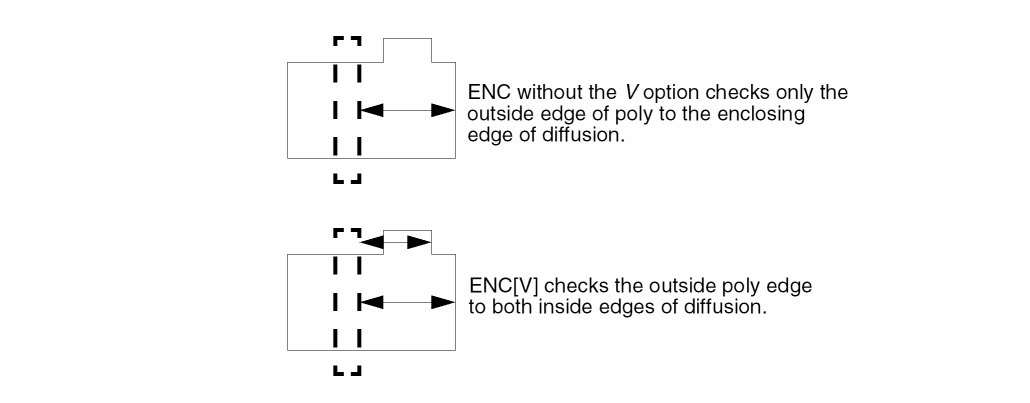
Filters out errors that are not at the end of the metal line. The [W] option turns on the [P] option automatically.
Checks the delta value in the x direction between two edges. The edges must project onto each other. Does not check non-Manhattan data.
Checks the delta value in the y direction between two edges. The edges must project onto each other. Does not check non-Manhattan data.
Layer Options
Checks the original layer, not the layer generated by the previous operation in the conjunctive rule. Use this option only with a conjunctive rule and on a layer with error flags.
Example 1
ENC layer1 layer2 LT 1 &
ENC layer1 layer3 LT 1 &
ENC layer1[0] layer3 LT 2 OUTPUT err1 2 3
Example 2
ENC[T] poly diff LT 4 OUTPUT drc03 51
ENC[T] diff poly LT 2 OUTPUT drc03 52
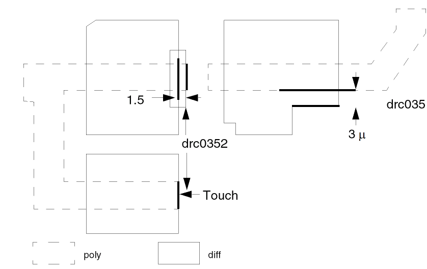
Example 3
This example checks for depletion (depl) completely enclosing or touching the transistor gate (xtor) in the direction of diffusion only.
AND     poly diff xtor
ENC[T]  xtor poly LT .001 &
ENC[TO] xtor depl LT 3 OUTPUT drc03 54
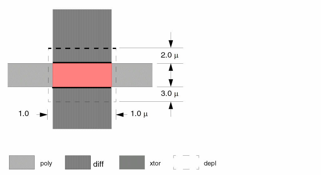
Example 4
This example checks for poly overlapping or touching diffusion (gate extension).
ENC[T] diff poly LT 2 OUTPUT drc03 52
Example 5
This example checks for poly that completely overlaps metal contact (mc) and for touch. Note in the example that if you include the E option, the metal contact outside is also flagged.
ENC[TO] mc poly LT 3 OUTPUT drc03 53
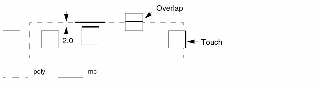
Example 6
ENC[T] xtor&xtorl poly LT .001 &
ENC[TO] &xtorl depl LT 3 OUTPUT drc03 54
Checks for depletion (depl) completely enclosing or enclosing and touching the transistor gate (xtor) in the direction of diffusion only.
The xtor layer is renamed &xtorl in the conjunctive rename operation, and now &xtorl contains the error flags from the joined operations. You can now use &xtorl in a further conjunctive operation:
ENC[TO] &xtorl enh LT 3 OUTPUT drc03 55
Checks for enhancement (enh) completely enclosing or enclosing and touching the transistor gate (xtor) in the direction of diffusion only. The conjunctive rename operation is optional but saves CPU resources.
Example 7
The following example outputs ptie (p+ diffusion in pwell) polygons enclosed by pwell less than 10 microns. The ptie polygons that touch the pwell inside-edge are also output. The output layer is badptie and is in trapezoid format.
ENC[T] ptie pwell SELLT 10 badptie
Example 8
The following example checks for diffusion (diff) enclosing metal contact (mc) on nonparallel edges. For example, rectangular contacts inside a diffusion area with its corners removed, having 45-degree edges.
ENC[C'] mc diff LT 2.5 OUTPUT drc03 57
Example 9
ENC[RO] deepn buried LT .001 dbcont
The dbcont are trapezoids with one resolution width specified in the Description block.
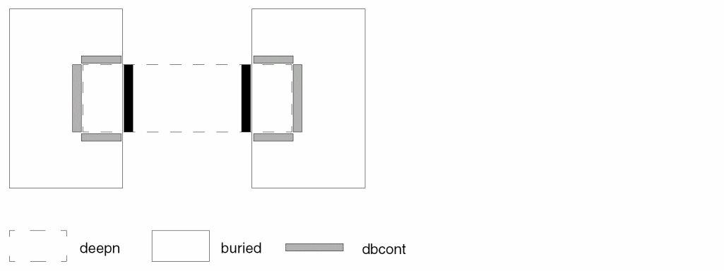
Example 10
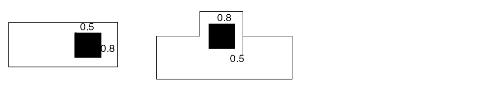
ENC via metal lt 0.5 output err 1
ENC[W] via metal lt 0.8 output err 2
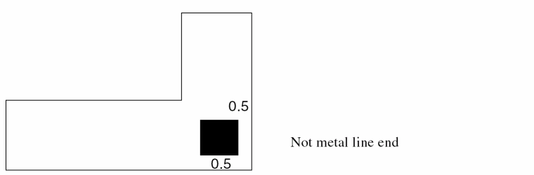
ENCBASEDOVLP
ENCBASEDOVLPlayer-alayer-b{trapfile} {OUTPUTc-namel-num}
FIXED-WIDTH width
TABLE = {
X1 Y1 W1
X2 Y2 W2
.....................
Xn Yn Wn
}
Description
Performs an overlap check based upon enclosure in the Dracula tool. Typically the command rules used to ensure a minimum intersection area of two layers are described in a table format and are lengthy, complicated, and numerous. In order to get complete coverage of the intent of the rules, it is common for a single rule to be expanded into tens or even hundreds of commands.
ENCBASEDOVLP efficiently performs a check of the rules in a table format, eliminates the need to write numerous complicated rules to achieve better performance from the check, and provides an accurate hierarchical check of overlap based upon enclosure.
The following definitions apply to overlap based upon enclosure checks:
-
Enclosed shape
A rectangular or polygonal shape that is of fixed width. -
Enclosing shape
The shape that encloses an enclosed shape. -
ENC-BASED-OVLP check
A minimum area intersection check in which a Y value measured from a specific intersection determines the minimums for X and W, where:- Y is the minimum enclosure distance of the enclosing shape over the enclosed shape in the direction perpendicular to the center line of the enclosed shape.
- X is the minimum overlap of the enclosing shape over the enclosed shape in the direction parallel to the center line of the enclosed shape.
- W is the minimum width of the enclosing shape measured in the direction parallel to the center line of the enclosed shape where they intersect.
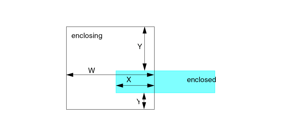
The following principles apply to the enclosing and enclosed shapes.
- The enclosed shapes are rectilinear shapes of fixed width.
- The enclosing shapes consist of edges that are either rectilinear or angled edges of 45 degree only.
- The X,Y, and W values required for this check are shown in the following table:
| RULE | X | Y | W |
|---|---|---|---|
where the X and W values are ascending and Y values are descending and all values are greater than or equal to 0.
The following is a geometric evaluation of the overlap area of the enclosing and enclosed shapes.
In the figure below, the overlap area of the enclosing and enclosed shapes has two sets of XYW values, {X1, Y1, W1} and {X2, Y2, W2}. If both sets of XYW values survive the test, the enclosed shape is good. If not, the ENCBASEDOVLP check reports a bad shape.
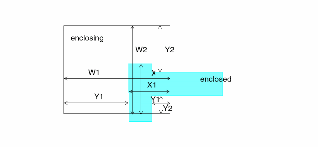
The following steps explain the algorithm for each set of XYW values.
-
Measure the minimum value
Y1of a given enclosed rectangular tile. For example, ifY1values are {0.19,0.08}, the minimumY1is0.08. -
In Table 13-1 given above, find the largest
Yvalue and proceed down the table through the descendingYvalues. Find the rule with theYvalue that most closely matches this minimum measuredY1 value. For example, ifY1 is0.88, rule800dis the closest match sinceY >= 0.80is the closest valid value. -
Measure
X1andW1. IfX1andW1meet the requirements of the rule, this is a good enclosed shape and the evaluation proceeds to the next shape.
Continuing with the previous example in which rule 800d is the closest match, the values ofXmust be>= 1.95andWmust be>= 2.75. If the values ofXandWare good, the shape is good and evaluation of the next shape begins.
If the first three steps fail to find a good overlap, return to step one and continue with the next set ofYmeasurements. If there are no moreYmeasurements, the shape is bad because a good overlap was not found.
The following is an output representation.
The intersection area of the enclosed shape and enclosing shape is the error representation. If the overlap check fails, the gray area shown in the figure below is written to the output layer as the error identification.
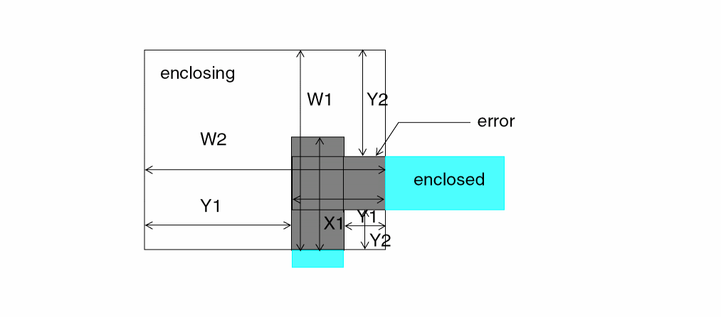
Arguments
Modifier used to direct the ENCBASEDOVLP check of the enclosing layer over the enclosed layer.
Layer that encloses the enclosed layer.
Layer that contains the enclosed shapes.
Trapezoid file name. Use this option only with the R or R' option or with SELLT, SELLE, SELGT, SELGE, or SELRA operations.
Sends the results to an output cell and writes the results of the DRC check to the outLayer layer name you specify.
c-name is the name of the output cell and can have six alphanumeric characters or fewer and no special characters and l-num is the cell layer number determined by your CAD system.
If your c-name is rule03 and l-num is 5, the output cell name is rule0305.
Specifies the fixed width of the enclosed shapes.
Specifies the minimum overlap of the enclosing shape over the enclosed shape in the directional parallel to the center line of the enclosed shape.
Specifies the minimum enclosure distance of the enclosing shape over the enclosed shape in the direction perpendicular to the center line of the enclosed shape.
Specifies the minimum width of the enclosing shape measured in the direction parallel to the center line of the enclosed shape where they intersect.
Examples
Syntax Example
The following example performs the ENCBASEDOVLP check on the enclosed shapes with a fixed width 0.5. The shapes are enclosed by the enclosing shapes according to the table below.
ENCBASEDOVLP MCB RX G190TR OUTPUT G190 62 FIXED-WIDTH 0.5
TABLE = {
0.85 0.35 0.60
0.85 0.20 0.65
0.90 0.15 0.75
1.05 0.10 0.90
1.20 0.05 1.20
1.30 0.00 1.30
}
|
Geometric Example
The following figure shows negative enclosure.
If the enclosed shape overlaps the enclosing shape such that a negative Y enclosure is measured, the ENCBASEDOVLP check follows the standard evaluation algorithm. The minimum Y is negative and the rule (from Table 13-2 above) with the Y value that most closely matches this minimum measured Y value is selected. Since the measured Y is negative, the last rule in the table is always selected.
A valid Rneg value must be placed at the last rule in the table and with the Y value exactly equal to the minus value of the fixed width of the enclosed shape. For example, if the width is 0.5, then the corresponding Rneg must be written as (x -0.5 w) and placed at the last row of the table. If the Y value of the last rule is not -0.5, then it is not thought as a valid Rneg value.
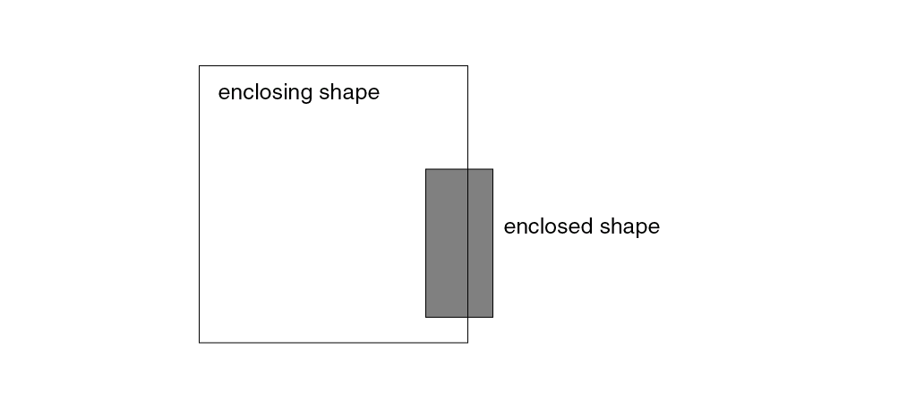
The following figure shows angled measurements.
If any measurement encounters an angled edge, the overlap is bad and an error shape is generated.
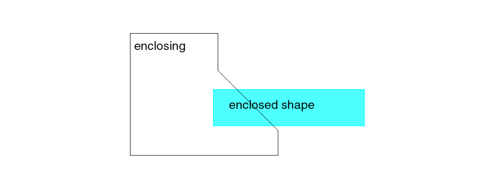
ENCRECT
ENCRECT LAYERlayer{NOT} RECTsize1size2{ANGLE450|1} {RESULTtrapfile} {OUTPUTcellnamelayernum datatype}
Description
This command determines which polygons on the specified layer enclose (or NOT enclose) rectangle with sides specified as size1 and size2.
Arguments
Keyword LAYER followed by the input layer name.
Sets checking for layer ploygons which do not enclose a rectangle of specified size.
Specifies a rectangle with sides of size1 and size2. The values are used as both horizontal and vertical sides.
0 | 1 Checks which layer polygons enclose (or do not enclose) the specified rectangle, with orthagonal sides only (‘0’), or also at 45 degree angles (‘1’). The default value of ANGLE45 is ‘0’ and does not check for non-orthagonal shapes. Specify “ANGLE45 1” to also check for rectangles at 45-degrees.
Specifies the output filename that contains the coordinates of polygons that enclose (or do not enclose) the specified rectangle.
Sends the results to an output cell of the specified cellname.
cellname is the name of the output cell and can have six or fewer alphanumeric characters and no special characters. layernum is the cell layer number.
The cellname and layernum are always concatenated. If your cellname is rule03 and layernum is 5, the output cell name is rule0305.
The datatype number associated with the layer number (layernum) of the output cell. Use datatype for GDSII only. Values can range from 0 to 63.
Example
ENCRECT LAYER metal RECT 100 200 RESULT layer1
ENCRECT LAYER metal NOT RECT 150 150 ANGLE45 1 OUTPUT res 1 1
EQUATION
EQUATION Kparameter=FORTRAN-expression{&}
Description
Specifies the equations that compute device parameters from extracted layout geometric primitive parameters or other computed parameters. Use this command in conjunction with the LEXTRACT command. Specify the parameter to compute and all EQUATION parameters in the PARSET command in the Description block. If you conjunct equations, EQUATION evaluates them sequentially. All referenced parameters in equations must be computed in previous equations.
Arguments
Specifies the fringe coefficient, and can apply to the same or different layer fringe extraction and overlap capacitance extraction with fringe consideration. You can use only DEPT and WIDT parameters as arguments. You must specify this equation first.
The following expressions are accepted:
|
LOG, EXP, MAX, MIN, SIN, COS, TAN, ASIN, ACOS, ATAN, SINH, COSH, TANH, SQRT, LOG |
Conjunction of several equations.
Note:-
A new function, INT now allows you to get the integer value from the EQUATION command. For example, this INT function allows you to output an integer value only of all resistors for contact in order to calculate the CONTACT numbers.
See “Example 3 - Using the INT Function” in this section for more information. -
The maximum length of an equation is 80 characters.
To include equations longer than 80 characters, use a continuation as shown in the following example. - In version 4.81 and subsequent versions, the ABS function is a new function that has been added to the list of functions used in the parameter expressions that this EQUATION command enables.
-
A new function, INT now allows you to get the integer value from the EQUATION command. For example, this INT function allows you to output an integer value only of all resistors for contact in order to calculate the CONTACT numbers.
Examples
EQUATION ca=0.00005*area+1.OE-4*(peri-ovpr)+1.4E-4*ovpr+
0.00005*area+1.OE-12*(2*peri-ovpr)+2.0
EQUATION ca=ca+4.5*(peri-ovpr)
Example 1
*DESCRIPTION
PARSET cap1 area peri ovpr c
.
.
*END
*OPERATION
AND met1 met2 m12
NOT met2 met1 mt
PARASITIC CAP[A] m12 met1 met2
LEXTRACT cap1 m12 met2 by cap[A] capout &
EQUATION c=0.00005*area+1.0E-4*(peri-ovpr)+1.4E-4*ovpr
Example 2
PARSET TCAP CLL TPR AREA PERI C
...
PARASITIC CAP[N1] M12 M1 M2
ATTRIBUTE 2.32 1.2 1.4 1.0
...
LEXTRACT TCAP M12 BY CAP[N1] L435BDT    &
EQUATION K= 2.875E-5+EXP(DEPT)+DEPT**2 &
EQUATION C= 2.32*AREA+ (PERI-TPR)+ CLL
For a discussion of flexible LPE parameter set extraction, refer to Chapter 7, “Extracting Electrical Parameters (LPE).”
Example 3 - Using the INT Function
EQUATION CNUM=INT((W-(2*M+CW))/(CW+CS)+1)
W is the width of resistor body.
M is the margin of the resistor head and contact.
CS is the space of the contacts.
Example 4 - Using the ABS Function
*.GLOBAL
*.BIPOLAR
*.RESVAL
*.SCALE
*.EQUATION
.PARAM
.SUBCKT test MINUS PLUS
Rrmfg1r0 PLUS MINUS
+(12.0+1.1*abs(2.34)) $[R1] $W=2u
.ENDS test
EXPLODE
EXPLODE{[A]} input-layer output-layer label
Description
Explodes Hcell shapes on the input-layer to the composite plane as
output-layer. Hcell input-layer shapes on nodes that connect to nodes in the composite plane are assigned the composite plane node ID in the output-layer. Other Hcell shapes on the input-layer (for example, those on nodes internal to the Hcell) are also exploded to the composite plane, but are assigned the node ID of label in the output-layer.
Arguments
Merges the exploded data with the composite data of input-layer to become the output-layer.
If you do not specify this option, Dracula explodes the cell instance data to the composite plane without merging the input composite data.
Sends the results to an output cell.
Name of the composite plane node in which to link to for shapes that form internal Hcell nodes.
Example 1
EXPLODE[A]   MET1  GMET1  VSS
AND          ME2   GMET1  CAP_M2M1  ;composite ME2 to all MET1
Example 2
EXPLODE      MET1  XMET1  VSS
AND          ME2   MET1   M2M1      ;comp ME2 to comp MET1
AND          ME2   XMET1  M2CM1     ;comp ME2 to cell MET1
EXT
EXT{[ ]} layer-a{&layer-a1}[ ] {layer-b{&layer-b1}}
LT/LE/EQ/RANGE/SELLT/SELLE/SELGT/SELGE/SELEQ/SELNE/SELRA n1 {n2}
{trapfile} {OUTPUT c-name l-num {d-num}} {&}
EXT[S{ }] layer-a{&layer-a1}[ ] {layer-b{&layer-b1}}
LT/LE/RANGE/SELLT/SELLE/SELGT/SELGE/SELRA n1 {n2} {CORNER-CORNER n2} {CORNER-EDGE n3}
{trapfile} {OUTPUT c-name l-num {d-num}} {&}
EXT[I] layer-a LT/LE n out-layer
Description
Checks the external separation between the outside edges of polygons. If you specify two layers, the Dracula product checks the outside edges of both layers against each other. If you specify one layer, the Dracula product checks the outside edges of that layer against each other.
Shell environment variables
-
setenv SPAC_LESS_SHIELD 1
Use this variable to disable violation checking of shielding, which can take significant time. Using this environment variable may significantly decrease runtime, but can also result in decreased accuracy in designs where there are many violations. -
setenv SPAC_LISTERR_DIGIT [ 2 | 3 ]
Use this environment variable to set number of digits after the decimal point for EXT/ENC/WIDTH/INT log report.
Checking Method
Flat, cell, hierarchical, and composite.
Arguments
Is the name of the first input layer.
Is the name of the second input layer.
Renames (conjunctive rename) the layer containing the error flags. The original layer name is then restored to the original layer. Do not put a space between the layer-a and &layer-a1 names, for example, poly&rpoly.
Renames in the same way as &layer-a1 except that it refers to layer-b.
Measures between the outside edge segments of polygons in layer-a and the outside edges of layer-b. Or, measures between the outside edges of layer-a if you only specify layer-a. Compares the measurements against the limits you specify and flags violations.
You must supply only one of these measurements:
Is the trapezoid file name. Use this option only with the R or R' option or with the SELLT, SELLE, SELGT, SELGE, or SELRA operations.
Sends the results to an output cell.
C-name: Is the name of the output cell and can have six alphanumeric characters or fewer and no special characters.
L-num: Is the cell layer number determined by your CAD system. If your c-name is rule03 and l-num is 5, the output cell name is rule0305.
Is the datatype number associated with the layer number (l-num) of the output cell. Use d-num for GDSII only. Values can range from 0 to 63.
Command Options
Options that are applicable to hierarchical Dracula are indicated with an ![]() icon in the margin. The plus (+) in an option adds error flags. The minus (-) in an option removes error flags.
icon in the margin. The plus (+) in an option adds error flags. The minus (-) in an option removes error flags.
Flags the actual part of a violation on a segment instead of the entire segment. This option can be applied only with LT or LE modifiers. Neither RA, GT, nor GE modifiers can contain the B option.
(-) Flags the edge-pair when the edges are parallel.
(-) Is the inverse of C option. Flags non-parallel edges.
(+) Flags a polygon that is totally enclosed by a polygon from another layer. See Example 14 Using the O, E, and G Options” in this section for more information.
Outputs error flags in trapezoid format that execute information for edge-sizing SIZE[E] operations.
Outputs error flags in trapezoid format. You must specify only trapfile name. It is similar to R option but does not turn on the P option.
(+) The G option is equivalent to using the O option along with the E option. This G option flags polygons that are fully enclosed by another layer as well as the cut off part of polygons enclosed by another layer. Error flags cover segments within layer-a and layer-b that outline the overlapping area of the two polygons. See “Example 14 Using the O, E, and G Options” in this section for more information.
(+) Flags the outside edges of notched layer-a polygons that fail the spacing check. A notch is a set of non-adjacent facing edges, or adjacent facing edges that create an external angle of less than 90 degrees. Use this option only with a single input layer.
Fills up the notches of a single layer automatically.
(-) Does not flag violations on polygons that are part of the same node. Use the CONNECT command to connect nodes before using this option. This option checks composite plane and cell plane nodal information, as well as nodal information between the composite plane and cell plane.
(-) Is the inverse of N option. Flags violations on polygons that are part of the same node, but not the same polygon. Use the CONNECT command to connect nodes before using this option. Checks composite plane and cell plane nodal information, as well as nodal information between the composite plane and cell plane.
(+) Flags layer-a and layer-b polygons that cut/overlap each other. Error flags cover segments within layer-a and layer-b that outline the overlapping area of the two polygons. The segments flagged are the segments of the trapezoids of these two polygons that cut the edges of the polygons. Does not flag a polygon that fully encloses a polygon of the other layer. See “Example 14 Using the O, E, and G Options” in this section for more information.
(-) Flags segments of edges that project onto each other. Two edges project if perpendicular lines from a referenced edge intersect the other edge. The referenced edge is the edge most closely aligned to the x or y axis.
(-) Is the inverse of the P option. Flags edges that do not project onto each other.
Outputs in trapezoid format the trapezoids enclosing the projection of violation flag pairs. A projected reference edge is the violation edge aligned closest to the x or y axis that projects orthogonally from that reference edge. You must specify the output layer only. Do not specify the OUTPUT error cell. Turns on the P option.
Outputs error flags in trapezoid format so you can reuse error data. You can process the created layer (from the error flags) with logical operations. The flags are one RESOLUTION unit wide (as specified in the Description block) and extend to the outside edge of the layers. Do not specify an OUTPUT error cell when you use this option. You cannot use this option with the R option.
(+) Flags violations on two polygons if edges of one polygon are within a “square boundary” and outside of the other polygon. When you use this option, you can also specify the CORNER-CORNER and CORNER-EDGE options. The default values for n2 and n3 are n1. If you do not specify the CORNER-CORNER option, n2 is set equal to n1. If you do not specify CORNER-EDGE option, n3 is set equal to n1. Use the following syntax for these options:
EXT[S] layer1 layer2 LT n1 {CORNER-CORNER n2} {CORNER-EDGE n3}
Only 90 degree angles are treated as "CORNER."
(+) Flags outside segments of layer-a polygons that touch outside segments of layer-b polygons. Reports edges and corners that touch.
Flags outside segments of layer-a polygons that touch outside segments of layer-b polygons at one point. Reports corners that touch.
(-) Does not flag violations on polygons that are part of the same node. Use the CONNECT command to connect nodes before using this option. This option checks only data on the composite plane.
(-) Is the inverse of U option. Flags violations on polygons that are part of the same node. Use the CONNECT command to establish nodal connectivity before using this option. This option checks only the data on the composite plane.
(+) Causes polygons to become visible through any inside surface shielding polygons. Inside surfaces of layer-a and layer-b are ignored.
EXT[V] = normal EXT + two layer inside shielding off (inside is visible) + single layer shielding off (visible through the layer itself)
(+) Causes polygons to become visible through any inside surface shielding polygons except the polygon itself.
EXT[V]’ = normal EXT + two layer inside shielding off (inside is visible)
EXT[V] A B LT 2 OUTPUT drc03 50
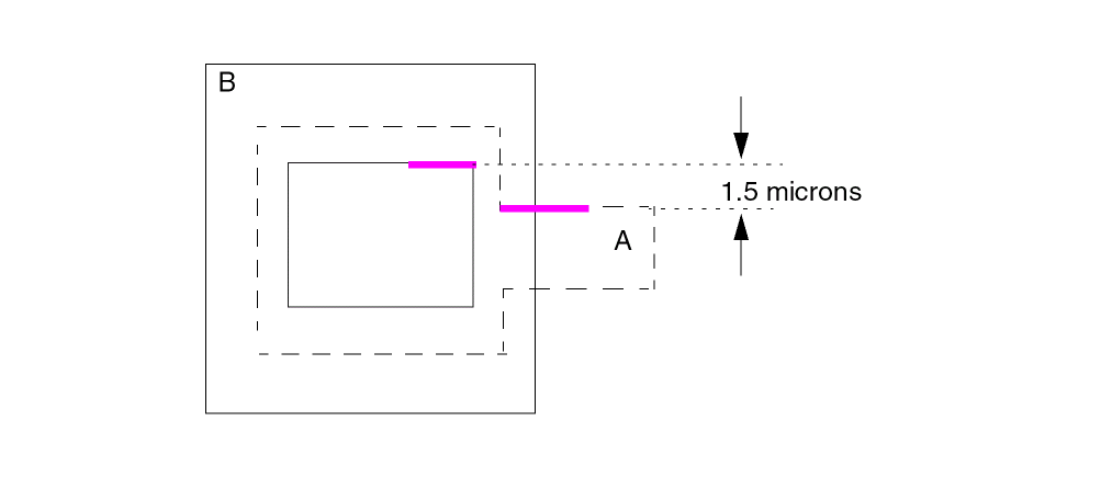
V, then the errors appear as shown in the above figure where the magenta-colored lines represent the errors. If the option is V’, then no errors appear.Checks the spacing value in the x direction between two edges. The edges must project onto each other. Does not check non-Manhattan data.
Checks the spacing value in the y direction between two edges. The edges must project onto each other. Does not check non-Manhattan data.
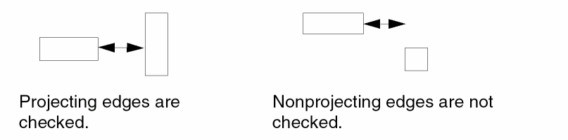
Outputs a fictitious region formed from the alignment point. This option must be used with the R option. When the error segment output by the R option is aligned in the X or Y axis, the region created has a zero projected area, and thus is left out of the final results. The region formed by the Z option extends both up and down by 1 dbu if the error segment is aligned along the X axis. The region extends to the left and right if the error segment is aligned along the Y axis.
Layer Options
Checks the original layer, not the layer generated by the operation in the conjunctive rule. Use this option only with a conjunctive rule and on a layer with error flags.
Example 1
EXT layer1 layer2 LT 1 &
EXT layer1 layer3 LT 1 &
EXT layer1[O] layer3 LT 2 OUTPUT err1 23
Example 2
CONNECT poly srcdrn BY cont
    EXT poly srcdrn LT 1 OUTPUT drc05 73
The error in the figure is a false error. It is not reported as a violation if the node option is flagged (that is, EXT [N] . . .).
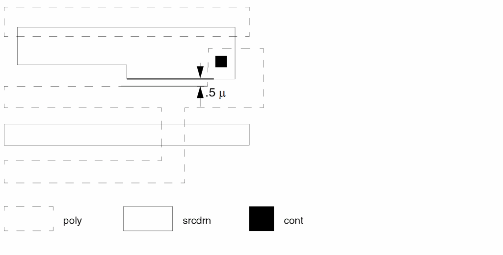
Example 3
EXT[R] poly metal LT 3 pmet
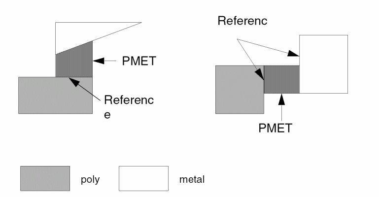
Example 4
This example checks for external spacing of metal, but metal carrying the same electrical node is not an error.
EXT[N] metal LT 5 OUTPUT drc05 70
Example 5
This example checks for gate external spacing to epi in the direction of diffusion only. Touching is also an error.
ENC[T] gate poly LT .001 &
EXT[T] gate epi LT 3 OUTPUT drc03 54
Example 6
ENC[T] gate&gatew poly LT .001 &
EXT[T] &gatew epi LT 3 OUTPUT drc05 55
This example also checks for gate external spacing to epi in the direction of diffusion only. Touch is also an error.
The layer gate is renamed to &gatew in the conjunctive rename operation, and now &gatew contains the error flags from the joined operations. You can now use &gatew in a further conjunctive operation.
EXT[T] &gatew mc LT 2 OUTPUT drc05 56
Checks for gate external spacing to metal contact (mc) in the direction of diffusion only. Touch is also an error.
The use of the conjunctive rename is optional but saves CPU resources.
Example 7
This example checks for metal to poly spacing and also for poly crossing metal at an acute angle. The reflection area must be clear by at least 2 microns. Flags the intersecting edges of two layers that form acute angles.
EXT metal poly LT 2 OUTPUT drc05 69
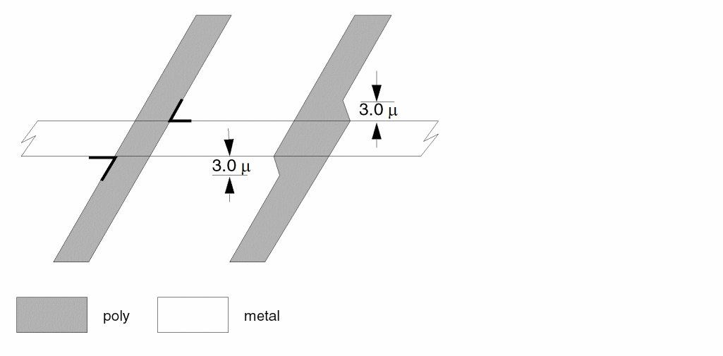
If you do not want the acute angles flagged, change the command to the following:
EXT metal poly RANGE 0 2 OUTPUT drc05 69
Example 8
This example checks for metal to poly spacing and does not flag poly crossing metal at an acute angle as in Example 5.
EXT metal poly RANGE 0 2 OUTPUT drc05 70
Example 9
This example checks for poly shapes spaced 3 microns from each other and for poly notches that are less than 3 microns.
EXT[H] poly LT 3 OUTPUT drc05 71
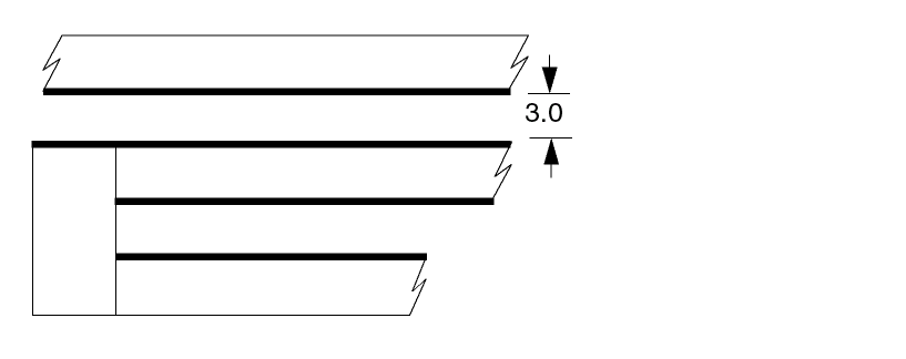
Example 10
This example outputs all psd (p+ source/drain) polygons that do not have any edges spaced less than or equal to 20 microns to pwell. The output layer is psd20 and is in trapezoid format.
EXT psd pwell SELGT 20 psd20
Example 11
This example outputs all ptie (p+ substrate tie-downs) polygons spaced greater than 40 microns from each other. The output layer, ptie40, is in trapezoid format.
EXT ptie SELGT 40 ptie40
Example 12
The following example checks for metal contact (mc) corner-to-corner spacing only. Corners that project onto adjacent corners are not checked.
EXT[P'] mc LT 2.5 OUTPUT drc05 72
EXT MET1 RA 1.61 2.11 OUTPUT DRC40
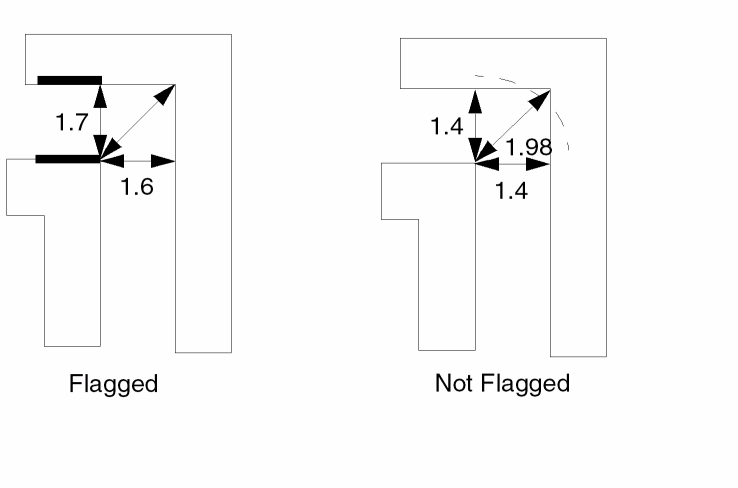
Example 13
The following example outputs errors between met1 shapes spaced less than 2 microns, including shapes with a corner-edge spacing box or a corner-corner spacing box of less than 2 microns.
EXT[S] met1 LT 2.0 OUTPUT DRC40
The following illustrates shapes that are in violation.
Example 14 Using the O, E, and G Options
The following example contains 4 figures.
- Figure 1 shows the EXT command by itself.
-
Figure 2 shows the EXT command with the O option, which does not flag polygons that are fully enclosed by another layer.
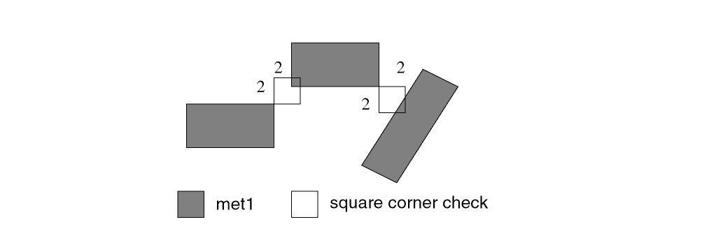
- Figure 3 shows the EXT command with the E option, which flags polygons that are fully enclosed by a polygon from another layer.
- Figure 4 shows the EXT command with the G option, which flags polygons that are fully enclosed by a polygon from another layer as well as the cut off part of polygons enclosed by another layer.
Example 14 - Figure 1
EXT A B LT 0.05 OUTPUT ERR 1 1
Example 14 - Figure 2
EXT[O] A B LT 0.05 OUTPUT ERR 1 1
Example 14 - Figure 3
EXT[E] A B LT 0.05 OUTPUT ERR 1 1
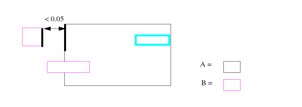
Example 14 - Figure 4
EXT[G] A B LT 0.05 OUTPUT ERR 1 1
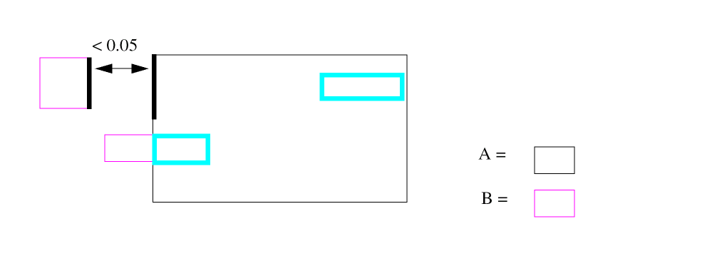
extractParasitic
extractParasitic(
   (   layers( layerList )
      cap( layer1 layer2 coefficientList {model(modelType)}
          {lateral(layerN piecewiseList)})
      |fringe( layer1 layer2 piecewiseList {mode1(modelType)}
         {equation("userEquation1")
         {equation("userEquation2") ...}}
         {parset(pName)})
      {cap|fringe(...)...}
   )
   (   ( resistor(resLayer sheetResValue {model(modelType)}
           {cont(contactLayerList)}
           {device(deviceLayerList)}
      {multiSheetRes piecewiseList}
      {model(modelType)}
           {maxlength(length)}
       {maxwidth(width)}
       {smash(smashResValue maxResValue)}
       {corner45(compenFactor)}
      {align}
      ) {resistor(...)...}

      ( contact(contactLayer layer1 layer2 contactCoefficient)
                        {model(modelType)})
      |   gateRes(subtype factor) {gateRes(...) ..}
   )
)
Description
Extracts parasitic resistance and capacitance (RC) from specified layers. For examples and a description of the types of parasitic RC you can extract, see the section about “Using One Function to Extract RC Parasitics” in the Dracula User Guide.
This command also can support parasitic diode command if you insert *dracrule and *endrule.
In version 4.7.0399 and later versions, an additional enhancement is that users can specify the model type for each capacitance or resistance command in extractParasitic(). PDRACULA will automatically generate the model commands with the correct subtypes.
The Spice files will include model type for resistors and capacitors.
*DESCRIPTION
MODEL = RES[subType1]modelType1RES[subType2]modelType2...
MODEL = CAP[subType3]modelType3RES[subType4]modelType4...
*END
*OPERATION
................
Arguments
Layers to be used for capacitor terminal layers. The layer list is a list of layer names or sublists. The maximum number of defined layers is 32. The format for this argument is as follows.
layers ( layer1 layer2 ( layer3 layer4...) ... )
The order of the list defines the geometric level of the layers. The first entry is considered the lowest level in the layout and the last entry is the highest level. The list is composed of at least two elements. The element can be a layer name or a layer sublist.
A layer sub-list consists of non-overlapping layers on the same geometric level in the layout. A layer sub-list must contain at least two layers.
Any layer in the list must be a connected layer or derived from a connected layer.
Layers involved in an extraction operation. For capacitance operations, they must be two different layers defined in the layer list.
Coefficients to use in the capacitance calculation. There are two forms.
areaCoeff perimeterCoeff
areaCoeff coCoeff upCoeff downCoeff
The user-specified model type for each capacitor or resistor or contact extraction command. The model option can be placed anywhere after the coefficient list, but before the lateral command for plate capacitor and after piecewise list or resistance coefficient for resistor or contact. PDRACULA will automatically generate model commands with correct subtypes.
The value to use for overlap area capacitance calculations.
The value to use for perimeter capacitance calculations.
The value to use for colinear edge capacitance calculations.
The value to use for sidewall-up capacitance calculations.
The value to use for sidewall-down capacitance calculations.
Specifies the fringe effect for an overlap capacitor.
Terminal layer for considering the possible fringe effect on the overlap capacitance.
User defined equation for fringe capacitance calculation. The syntax for equation is the same as the syntax for EQUATION command.
User defined parset name. The default parset name used in LEXTRACT when equation command is used in extractParasitic is CAPF. If the equations contain parameters other than C, WIDTH,DEPT and K, user-defined parset name is required. When parset is specified, PDRACULA uses pName in the expanded rule file instead of the default one.
For capacitance, this is a list of coefficient pairs defining the piece-wise fringe capacitance. The list has the following form:
(separationRange fringeCoeff)
When the separation of two layers is below the separationRange, the corresponding fringeCoeff is applied as the unit length capacitance value.
For resistance, this is the list of width, sheet resistance value pairs for multiSheetRes option. This list has the following form:
((width1 sheetResValue1) (width2 sheetResValue2)... (widthn sheetResValuen))
Assume W1 and W2 is the width on the two side of a resistor body, (see Chapter 9, Extracting Parasitic Resistance (PRE)) and width=max(W1,W2),
0 < width <= width1, use sheetResValue1 as sheet resistance
width1 < width <= width2, use sheetResValue2 as sheet resistance
width(n-1) < width <= widthn, use sheetResValuen as sheet resistance
Weffective=(W1+W2)/2 L=AREA/Weffective
R = sheetResValuen * L/Weffective
In the following example, if multiSheetRes is used, width for resistor R1 is w1 and width for resistor R2 is w2. The effective width of R1 is w1 and of R2 is (w1+w2)/2.
Name of the parasitic resistor layer. This layer must be defined in a CONNECT-LAYER command.
Sheet resistance value in units per square, where the units correspond to the resistance units specified in the UNIT command.
One or more contact layers to use in the contact resistance capacitance calculation. If you do not specify a contact layer, the function searches the contacts of all resLayers used in CONNECT commands.
One or more device terminal layers belonging to resLayer. If you do not specify a device layer, the function will search all gate layers used in ELEMENT MOS and ELEMENT LDD commands.
Maximum length of a parasitic resistor device in a number of squares. If a resistor device exceeds this maximum, the resistor is partitioned into multiple devices evenly.
Each resistor device that is formed is smaller than the maximum value, and the values are distributed evenly on the resistor. The maximum difference between two sections is one. For example, if the resistor body is 91, and you specify a maximum length of 20, the sections are 19, 18, 18, 18, and 18.
Value used by the WIDTH command within the command sequence CUT-TERM runs. For an example of how CUT-TERM uses the WIDTH command and maximum width value, refer to the “Example” in the CUT-TERM section. Default is 40.
Resistance value used as a threshold. Series resistors with values below smashResValue are smashed.
Maximum value of a resistor that results from smashing serial parasitic resistors. This prevents the Dracula software from creating a big resistor from subsequent smashing.
Argument used for compensating resistance in 45-degree terminals.
The terminal cut aligns with the context edge if you specify this argument for resistor.
Layer to use in the contact resistance calculation.
The connection layers of the contact.
Value to use for contact resistance calculations. The default equation is
R =contactCoefficient/contactArea
MOS element and subtype in which you want to extract gate resistance.
Gate resistance factor, which is used as
R = factor * (w / L)
For PRE cases, the Dracula rule embedded inside *dracrule and *endrule is put behind re-extraction elements in the expand rule file. You can use this function to do parasitic diode extraction composite with the extractParasitic() command.
Example 1
extractParasitic(
( layers( BULK (NWELL PWELL)(PSD NSD POLY) MET MT2)
fringe(MET1 MET1 (1.0 0.02)(1.5 0.015)) ; 1-layer fringe
fringe(MET1 MET2 (1.0 0.03)(1.5 0.01)) ; 2-layer fringe
cap (BULK POLY 0.35 0.12); poly, substrate overlapped cap
cap (BULK MET1 0.4 0.15) ; met1, substrate overlapped cap
cap (POLY MET1 0.2 0.3 ; 2D3B model for overlapped cap
   lateral(POLY (1.0 0.03)(1.5 0.02)))
cap (POLY MET2 0.3 0.02 0.1 0.15)) ; sidewall cap
( resistor(MET1 0.1 cont(CONTACT VIA))
resistor(MET2  0.3 cont(VIA) maxlength(30))
resistor(POLY 0.7 cont(CONTACT) device(NGATE PGATE))
contact(VIA MET1 MET2 0.1)))
Example 2
extractParasitic(
*dracrule
; Define Parasitic Junction Diodes
NOT    SUB     NWZ    PSUB
AND    PDIFC   NWZ    PDIO  ; p+ diode trm to nwell less p+ ties
AND    NDIFC   PSUB   NDIO  ; n+ diode res to psub less n+ ties
AND    RDIFC   PSUB   RDIO  ; n+ diode res to psub less n+ ties
;
PARASITIC  DIO{PT} PDIO     PDIO    NWZ     ; pdiff/n-
PARASITIC  DIO{NT} NDIO     PSUB    NDIO    ; ndiff/p-
PARASITIC  DIO{RT} RDIO     PSUB    RDIO    ; ndiff/p-
;
*endrule
(
   layers(SUB NWZ  (NDIF PDIF) PCZ MCZ  M1BIAS M2BIAS )
   fringe(PCZ    PCZ    (0.32 3.972670e-06) (0.86 2.434180e-06))
   fringe(MCZ    MCZ    (0.26 2.751891e-05) (0.80 2.514589e-05))
   fringe(M1BIAS M1BIAS (0.35 2.154846e-05) (0.98 1.084768e-05))
   fringe(M2BIAS M2BIAS (0.40 2.712161e-05) (1.21 1.412467e-05))
   .
   .
   cap(SUB NWZ       1 0.9 0.8 0.7)
   cap(SUB NDIF      1 0.9 0.8 0.7)
   cap(SUB PDIF      1 0.9 0.8 0.7)
   cap(SUB PCZ       1 0.9 0.8 0.7)
   cap(SUB MCZ       1 0.9 0.8 0.7)
   .
   .
   .
)
(
   resistor(PCZ 7.0E-3 cont(MCDIF MCPC) device(PDEVICE NDEVICE
      RGATER LWGATE XWGATE ZGATE NWCON) smash(0.0E-3 5.0E-3))
   resistor(MCZ 0.24E-3 cont(MCDIF MCPC CNTALL) smash(0.0E-3 0.5E-3))
   resistor(M1BIAS 0.061E-3 cont(CNTALL V1ALL) smash(0.0E-3 0.05E-3))
   resistor(M2BIAS 0.061E-3 cont(V1ALL V2ALL) smash(0.0E-3 0.05E-3))
   .
   .
   contact(MCDIF MCZ NDIF 1     )
   contact(MCDIF MCZ PDIF 1     )
   .
   .
))
   .
   .
   .
;***************************************************************
; Parasitic diode extraction formula
;***************************************************************
LEXTRACT        MDIF    PDIO    PDEVN BY DIO[PT] PTDIF &
EQUATION        P1=PERI-OVPR &
EQUATION        A1=AREA
;
LEXTRACT        MDIF    NDIO    NDEVN BY DIO{NT} NTDIF &
EQUATION        P1=PERI-OVPR &
EQUATION        A1=AREA
;
LEXTRACT        MOSF    RDIFC   RDEVN BY NODE RMDIF &
EQUATION        PERI=PERI-OVPR

   .
   .
   .
Example 3
extractParasitic(
( layers( BULK (NWELL PWELL)(PSD NSD POLY) MET MT2)
fringe(MET1 MET1 (1.0 0.02)(1.5 0.015)
equation(“C=(19.761/(DEPT+4.2))*WIDT*0.001”)) ; 1-layer fringe
fringe(MET1 MET2 (1.0 0.03)(1.5 0.01)) ; 2-layer fringe
cap (BULK POLY 0.35 0.12); poly, substrate overlapped cap
cap (BULK MET1 0.4 0.15) ; met1, substrate overlapped cap
cap (POLY MET1 0.2 0.3 ; 2D3B model for overlapped cap
   lateral(POLY (1.0 0.03)(1.5 0.02)))
cap (POLY MET2 0.3 0.02 0.1 0.15)) ; sidewall cap
( resistor(MET1 0.1 cont(CONTACT VIA)
   multiSheetRes((0.05 0.15) (0.1 0.1)) model(RR1))
resistor(MET2 0.3 cont(VIA) model(RR2) maxlength(30))
resistor(POLY 0.7 cont(CONTACT) device(NGATE PGATE) model(RR3))
contact(VIA MET1 MET2 0.1)))
FLATTEN
FLATTEN layer-a trapfile
Description
Flattens Hcell data and places it in a flattened layer. In flat Dracula, the FLATTEN command copies one layer to another.
Checking Method
Hierarchical, composite, and flat.
Arguments
Name of the input layer or a generated layer in hierarchical Dracula.
Name of the trapezoid file. The trapfile name can have up to seven alphanumeric characters and no special characters. The first character must be a letter.
In flat Dracula, trapfile consists of trapezoid data that is an exact copy of data from layer-a.
In hierarchical Dracula, use this command for operations that cannot be done on hierarchical layers, such as HDRC SELECT LABEL, which requires nodal information. You can also run HDRC checking commands with large dimensional checks (for example, 10 microns) without penalizing performance or disk space for the other HDRC checking commands.
Note: Layer-a must be a hierarchical (unflattened) layer. If you use the command in a check-mode other than hierarchical mode, Dracula copies only layer-a to trapfile. Therefore, if you change check-mode from hierarchical to flat, you do not have to edit the rules file.
Example 1
FLATTEN cont cont1
In flat Dracula, layer cont1 consists of the data from cont. You can now use cont1 in any Operation block command. In hierarchical Dracula, cont is a hierarchical layer and cont1 is the flattened layer.
Example 2
FLATTEN PSUB PSUB1
NOT PSUB1 PSUB PSUBX      ;; PSUBX contains exploded cell data
LINK PSUBX TO GND         ;; link cell data to ground
AND MET2 PSUBX M2SUBX     ;; MET2 to cell PSUB overlap
AND MET2 PSUB M2SUB       ;; MET2 to composite PSUB overlap
FLOATCHK
FLOATCHKcontact-layer{trapfile} OUTPUTc-name l-num{d-num}
Description
Finds floating contact geometries on the contact layer you specify. A floating contact is any contact, or part of a contact, not covered by both connect layers defined in the CONNECT command.
Arguments
Name of the contact layer. The contact-layer must be a contact used in a CONNECT command.
Name you designate as the output file to contain composite trapezoids.
Sends the results of the operation to an output cell.
C-name is the name of the output cell and can have six alphanumeric characters or fewer and no special characters. L-num is the cell layer number determined by your CAD system.
If your c-name is rule03 and l-num is 5, the output cell name is rule0305.
Datatype number associated with the layer number (l-num) of the output cell. Use d-num for GDSII only. Values can range from 0 to 63.
Example
FLOATCHK CONT OUTPUT CONT1 23
FLOATCHK PCONT OUTPUT PCONT2 23
FLOATCHK NSUB OUTPUT NSUB3 23
FRINGE CAP
FRINGE [options] CAP [type]layer-a layer-b
Description
Defines the fringe capacitance of the same or different layers. Use an ATTRIBUTE CAP command after the FRINGE CAP command. ATTRIBUTE CAP associates the geometry data with the process-dependent electrical properties. ATTRIBUTE CAP does not accept units. The scale of the FRINGE CAP attribute must match the scale of the layout database.
Fringe capacitors apply to stray capacitances between two nodes on the same or different conductor layers. This command does not extract capacitances if both terminals are at the same node.
For overlapping fringe capacitance extraction, only the overlapping edges of the two input layers are considered.
The default mode of the FRINGE CAP command uses shielding. For example, in the following graphic, shape1 of MET1 shields part of POLY from shape2. When calculating fringe capacitance, the shielded part is not neglected.
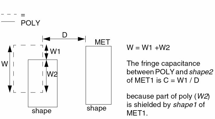
FRINGE CAP with PRE
Use the FRINGE CAP command with PRE. Resistor device layers for PARASITIC RES are allowed as terminal layers for FRINGE CAP. In general, these resistor device layers have no nodal information.
If the first terminal layer in a FRINGE CAP command is a PARASITIC RES device layer, the FRINGE CAP device layer does not need nodal information.
Arguments
Can be from among the following:
Type of fringe CAP device. The first character must be a letter from A to Z. The second character is optional and can be any letter from A to Z or any number from 0 to 9 (except 8). This code differentiates between fringe capacitor devices.
Terminal conductor layer. This layer is the conductor layer for one side of the capacitor and must carry node information.
Terminal conductor layer. This layer is the conductor layer for the other side of the capacitor (can be the same or different from layer-a) and must carry node information.
Example 1
FRINGE[R] CAP[A] M1RES M1TRM
ATTRIBUTE CAP[A] 5 0.000027
Example 2
AND L3 L5 L3L5
FRINGE[S] CAP[L] L3L5 L3
ATTRIBUTE 1.0 0.002
ATTRIBUTE 1.5 0.0003
Example 3
In the following example, layer PAOM1 is derived from MET1. POAM1 is also a subset of MET1. To prevent calculating capacitance from false edges of POAM1 (edges of shapes from POAM1 that do not overlap with shapes of MET1, for example, edges within shapes of MET1), you use the [S] option.
AND POLY MET1 POAM1
FRINGE[S] CAP POAM1 MET1
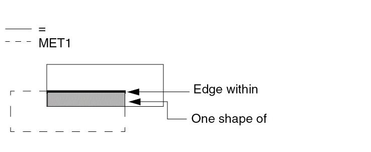
Example 4
In the following example Dracula supports zero distance FRINGE CAP.
FRING CAP[A] MET1 MET2
ATTRIBUTE CAP[A] 0 0.000005 ; DEPTH = 0
ATTRUBUTE CAP[A] 0.6 0.000005 ; 0 < DEPTH <= 0.6
ATTRUBUTE CAP[A] 1.2 0.000003 ; 0.6 < DEPTH <= 1.2
ATTRUBUTE CAP[A] 1.8 0.000002 ; 1.2 < DEPTH <= 1.8
C = K x (WIDTH / DEPTH) when DEPTH !=0
C = K x WIDTH when DEPTH =0
GENRECT
GENRECT input-layer XYLEN xl yl XYGAP xg yg {XYADJ xa ya} trapfile
Description
Generate rectangle shapes that overlap input layer, flat mode only. In version 4.81 and later versions, Dracula provides a new option for generating a staggered pattern rectangle array for area fill, as shown in the following figure.
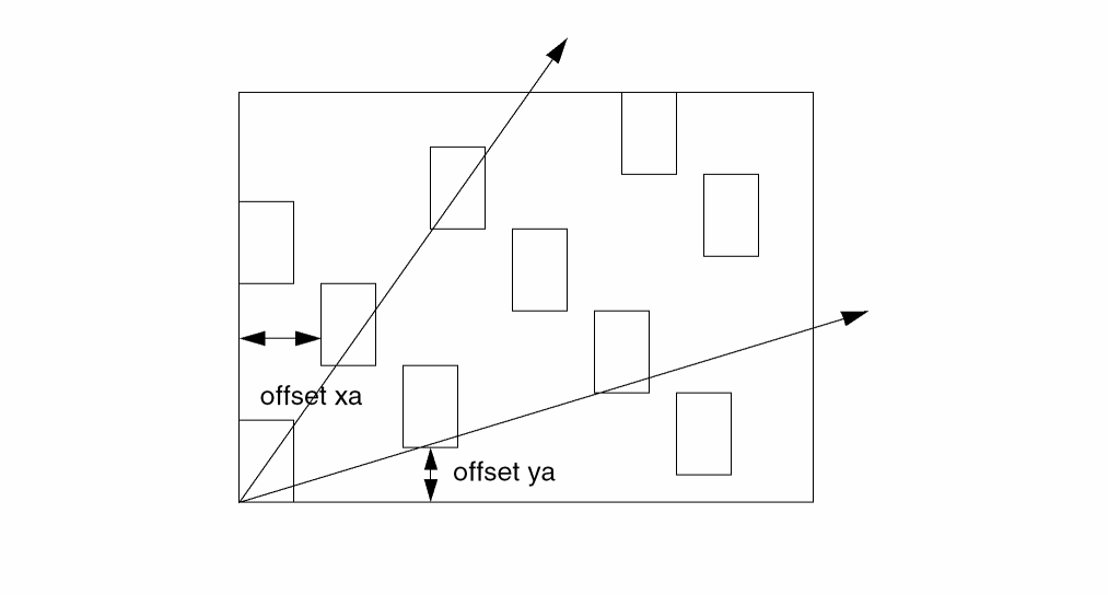
Arguments
Generate each rectangle with XY-axes offset
Example
GENRECT errwin XYLEN 2.0 3.0 XYGAP 1.0 2.0 XYADJ 1.0 1.0 fill
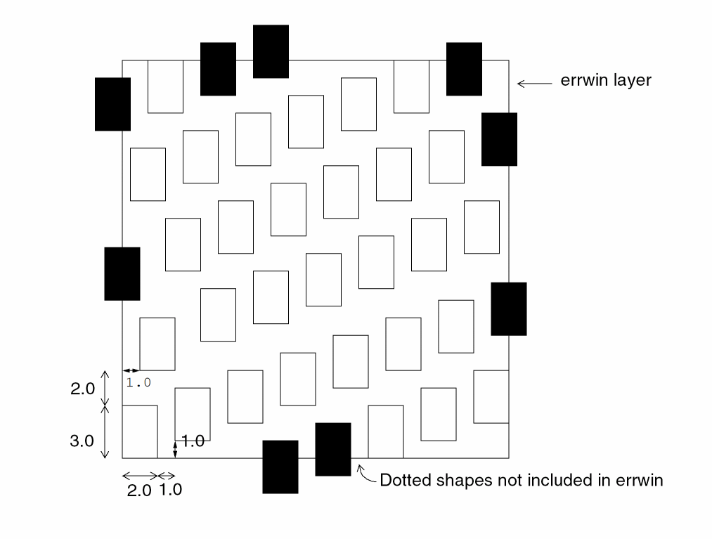
GLOBAL-SCONNECT
GLOBAL-SCONNECT = YES/NO
Description
Specifies a global majority rule for SCONNECT. Dracula uses the local majority to determine the node within the local lower region, and it uses the global majority to determine the node within all lower regions. If, after considering these majorities, Dracula cannot decide the winning node, it chooses the node with the smallest node number.
Arguments
Activates global majority rule for SCONNECT conflict resolution.
Specifies random choice for SCONNECT conflict resolution. Default.
Example
In the following example, Region1 is stamped Node2.
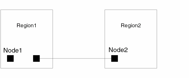
GPATHCHK
GPATHCHK  {[options]}  LEVEL  n  {trapfile} OUTPUT  c-name
l-name  {d-num}
Description
Checks for nodes that should have a path to both power and ground through one or more terminals of transistors, diodes, or resistors. This command assigns an error code to nodes without a proper path to either power or ground.
Before using GPATHCHK, you must use the GPATHDEF command to define the connectivity flow for your devices. For details, refer to the
Arguments
Can be from among the following:
Specifies the name of a trapezoid data file to be generated.
Sends the results of the operation to an output cell.
C-name is the name of the output cell and can have six alphanumeric characters or fewer and no special characters. L-num is the cell layer number determined by your CAD system. If your c-name is rule03 and l-num is 5, the output cell name is rule0305.
Datatype number associated with the layer number (l-num) of the output cell. Use d-num for GDSII only. Values can range from 0 to 63.
GPATHDEF
GPATHDEFelem{[type]}nodetype-1FROMlayer-aTOlayer-b{WHENlayer-c nodetype-2}
Description
Defines the device power and ground connectivity flow path. Each GPATHDEF command specifies an element type and a rule for the directional flow through the device. After you define the flow rules, use the GPATHCHK command to check the paths.
There are several standard rules that you do not need to specify. For example, MOS and RES elements pass power and ground signals in both directions. If necessary, you can redefine the rules for the MOS or RES elements.
The GPATHDEF command must specify the full device type with subtype if you specify an ELEMENT command. You cannot have generic rules for device types because the layers are different for each device type.
Arguments
Specify one of the following element types:
MOS for a MOS device
BJT for a bipolar device
DIO for diodes
The two-letter (A-Z) code that denotes the device type. This code can differentiate N-channel from P-channel in CMOS or differentiate MOS devices with different implants.
The type of node that flows through the device in this direction. Specify POWER or GROUND.
The conducting layer for the terminal into which nodetype-1 flows.
The conducting layer for the terminal from which nodetype-1 flows.
If you specify this option, the flow occurs only when the conditions you specify for layer-c or nodetype-2 are true. Otherwise, the flow always occurs.
The conducting layer for the terminal that controls the flow through the device.
The type of node that enables the flow through this device. Specify POWER or GROUND.
Examples
GPATHDEF BJT POWER FROM COL TO EMIT WHEN BASE POWER
GPATHDEF BJT GROUND FROM EMIT TO COL WHEN BASE POWER
GPATHDEF BJT GROUND FROM EMIT TO BASE
GPATHDEF BJT POWER FROM EMIT TO EMIT
GPATHDEF BJT POWER FROM EMIT TO EMIT
The following example describes the diode rules:
GPATHDEF DIO POWER FROM ANODE TO CATHODE
GPATHDEF DIO GROUND FROM CATHODE TO ANODE
The following example defines the default MOS and RES rules:
GPATHDEF MOS POWER FROM SRCDRN TO SRCDRN
GPATHDEF MOS GROUND FROM SRCDRN TO SRCDRN
GPATHDEF RES POWER FROM RTERM TO RTERM
GPATHDEF RES GROUND FROM RTERM TO RTERM
GROW
GROWinput-layer dx dy{dx2 dy2}trapfile{OUTPUTc-name l-num{d-num}}
Description
Oversizes a single side of a layer. The dx and dy values determine the direction and amount of growth. You can specify two different directions within a single command.
For more information about sizing geometries, refer to the SHRINK.
Arguments
The amount you want to size the layer. This value is a real number in microns or mils. This is the unit set by the SCALE command.
Specifies a second size amount. All values must be positive.
The name of the trapezoid file.
The name of the output cell to which you can optionally output the sized data.
The layer number of the output cell.
The datatype number associated with the layer number (l-num) of the output cell.
Examples
*DESCRIPTION
SCALE = 0.001 MIC
RESOLUTION = 0.001 MIC
*END
*OPERATION
...
GROW lay1 -0.5 -0.0 lay2 ;Grow left edge 0.5 microns
...
GROW lay5 0.25 0.25 lay6            ;SIZE MEBES data in
RELOCATE lay6 BY -0.125 -0.125 lay7 ;layf by 0.125,which
*END
HEDTEXT
HEDTEXT = file-name
Description
Specifies the Hcell text file name. This command is similar to the EDTEXT command, except it is used for texting hierarchical cells. Use this command to attach Hcell pin texts to Hcell pins.
Each statement in the file must have the following items:
- The text name
-
The x and y coordinates
These coordinates are relative to Hcell coordinates. The x and y are not case sensitive. - The name of the Hcell
Optionally, you can use ATTACH parameter to indicate the layer to which to attach the text. If you do not specify ATTACH, the text is attached according to the CONNECT-LAYER reference.
The file accepts a tab as a delimiter. You can use a semicolon (;) to start a comment. The comment must be on its own line. You can put the comment starter (;) in the first column of a line, or you can precede it with blank spaces. You cannot put a comment at the end of a line of text in an HEDTEXT file. The Dracula program ignores all text after the comment starter. You can also use a blank space in place of an equal sign (=).
Checking Method
Example
hedtext abc.htx
VDD    x=56    y=89   inv
VSS    x=6     y=40   ATTACH=met    inv
IN     x=41    y=90   ATTACH=poly   inv
OUT    x=89    y=44                 inv
VDD    x=123   y=96   ATTACH=met    nand
HIERARCHEN
HIERARCHEN flayer-name hlayer-name
Description
Converts a flattened layer to a hierarchical layer.
Checking Method
Arguments
The name of a flattened layer generated by a prior FLATTEN command.
The hierarchical version of flayer-name. This layer has the same Hcells as before the FLATTEN command was issued.
If you use this command in a mode other than hierarchical, Dracula makes a copy of only layer flayer-name to layer hlayer-name. Therefore, if you change check mode from hierarchical to flat, you do not have to edit the rules file.
Example
HIERARCHEN fmetal hmetal
HOLE
HOLE {[options]} layer-a {x_boundary y_boundary} trapfile
Description
The HOLE command extracts holes for the specified layer and forms a new layer for later related DRC checking. This command always selects the holes region by region. Thus the region number assigned by the Dracula tool affects the results of the HOLE command.
Arguments
Treats two polygons with only their corners touching as the same region and selects the correct holes.
Generates innermost holes that contain no internal holes, but may contain layer-a shapes.
Generates innermost empty holes that contain neither internal hole nor other layer-a shapes. The output is subset of [I] option.
Generates outermost holes that can contain both the internal holes and layer-a shapes, but can not be inside of other hole.
Generates a subset of [O] option, which has no layer-a shapes inside the hole and is not inside of other hole.
Specified layer to extract holes.
Optionally specified filter box boundary.
Output layer that contains holes of layer-a
Example 1
HOLE metal 10 10 smet
Layer smet contains shapes that extract holes of the input layer metal as seen in the following figure.
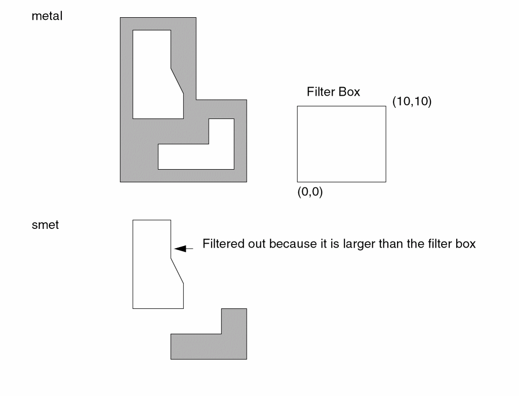
Example 2
By default, the Dracula tool treats two polygons touched by only the corner points as different regions. In the following figure, the corner-touched polygons are treated as different regions (region #1 and region #2).
HOLE metal 10 20 smet
Using the above rule and layout, layer smet is empty.
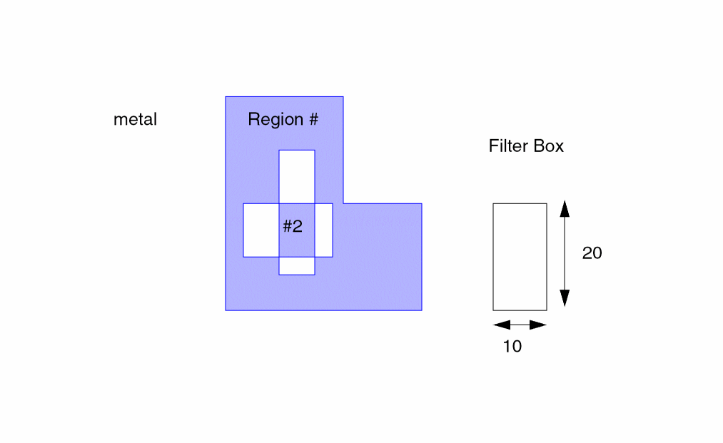
A new option in the Dracula 4.9 release, the option C for HOLE treats two polygons touched by only the corner points as the same region as illustrated in the following figure.
HOLE[C] treats two polygons touched by only corner points as the same region and so can extract correctly the holes inside layer metal.
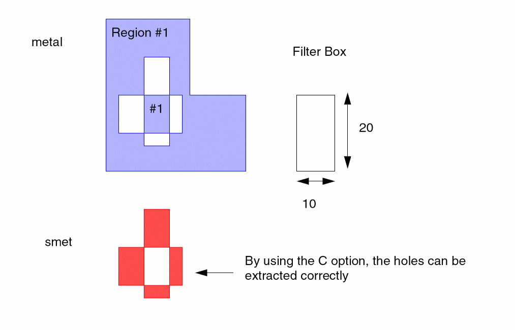
Example 3
The following example illustrates how do I, I’, O and O’ options work:
HOLE[I] INLAY IMOST
HOLE[I’] INLAY IMOSTE
HOLE[O] INLAY OMOST
HOLE[O’] INLAY OMOSTE
Figure below shows INLAY and 4 different results of the command above.
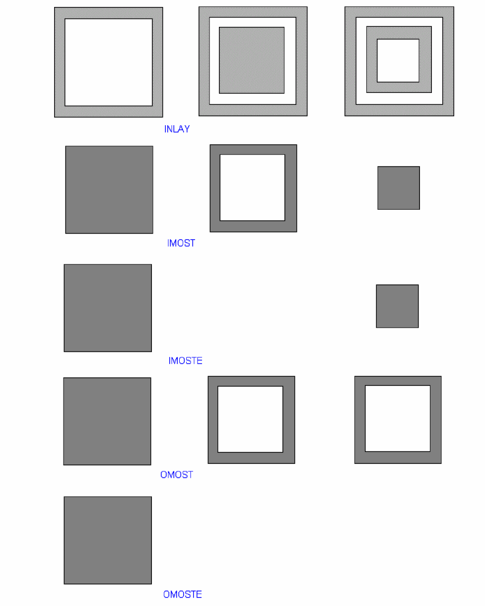
INT
INT{[ ]} layer-a{&layer-a1}[ ]  layer-b{&layer-b1}
LT/LE/EQ/RANGE/SELLT/SELLE/SELGT/SELGE/SELEQ/SELNE/SELRA n1 {n2} {trapfile} {OUTPUT c-name l-num {d-num}} {&}
Description
Determines the depth to which polygons of two layers overlap. This command measures between the inside edges of polygons.
Shell environment variables
-
setenv SPAC_LISTERR_DIGIT [ 2 | 3 ]
Use this environment variable to set number of digits after the decimal point for EXT/ENC/WIDTH/INT log report.
Checking Method
Flat, cell, hierarchical, and composite.
Arguments
The name of the first input layer.
The name of the second input layer.
Renames (conjunctive rename) the layer containing the error flags. The original layer name is then restored to the original layer. Do not put a space between the layer-a and &layer-a1 names, for example, poly&rpoly.
Same as &layer-a1 except that it refers to layer-b.
Measures between the polygons of layer-a that overlap polygons of layer-b. (Note: Overlapping is a commutative relation; that is, if A overlaps B, then B overlaps A.) Measures from inside segments of layer-a to inside segments of layer-b for segments that do not coincide.
Flags violations after comparing the measurements against the limits you specify, such as:
The name of the trapezoid file.
Sends the results to an output cell. The output cell contains clean polygons in polygon format, resulting in reduced trapezoid construction lines and a more compact cell.
R
R’
SELLT
SELLE
SELLGT
SELLGE
SELLRA
SELEQ
SELNE
C-name is the name of the output cell and can have six alphanumeric characters or fewer and no special characters. L-num is the cell layer number determined by your CAD system. If your c-name is rule03 and l-num is 5, the output cell name is rule0305.
The datatype number associated with the layer number (l-num) of the output cell. Use d-num for GDSII only; values can range from 0 to 63.
Ampersand sign indicates a conjunctive rule.
Command Options
Options applicable to hierarchical Dracula are indicated with an ![]() icon in the margin. A plus (+) in an option adds error flags. A minus (-) in an option removes error flags.
icon in the margin. A plus (+) in an option adds error flags. A minus (-) in an option removes error flags.
Flags the actual part of a violation on a segment instead of the entire segment. This option can be applied only with LT or LE modifiers. Neither RA, GT, nor GE modifiers can contain the B option.
(-) Flags the edge pair when the edges are parallel.
(-) Inverse of C option. Flags nonparallel edges.
Outputs error flags in trapezoid format that execute information for edge-sizing SIZE[E] operations.
Outputs error flags in trapezoid format. You must specify only trapfile name. It is similar to R option but does not turn on the P option.
(-) Does not flag violations on polygons that are part of the same node. Use the ONNECT command to connect nodes before using this option. This option checks composite plane and cell plane nodal information, as well as nodal information between the composite plane and cell plane.
(-) Inverse of N option. Flags violations on polygons that are part of the same node. Use the CONNECT command to connect nodes before using this option. Checks composite plane and cell plane nodal information, as well as nodal information between the composite plane and cell plane.
(-) Flags segments of edges that project onto each other. Two edges project if perpendicular lines from a referenced edge intersect the other edge. The referenced edge is the edge most closely aligned to the x or y axis.
(-) Inverse of P option. Flags edges that do not project onto each other.
Outputs in trapezoid format the trapezoids enclosing the projection of violation flag pairs. You must specify the only output layer. Turns on the P option.
Outputs error flags in trapezoid format so you can reuse error data. You can process the created layer (from the error flags) with logical operations. The flags are one resolution unit wide (as specified in the Description block). You cannot specify an output error cell.
(+) Flags violations on the two polygons if the edges of one polygon are within a “square boundary” and inside the other polygon. When you use this option, you can also specify the CORNER-CORNER and CORNER-EDGE options. The default values for n2 and n3 are n1. If you do not specify the CORNER-CORNER option, n2 is set equal to n1. If you do not specify CORNER-EDGE option, n3 is set equal to n1.
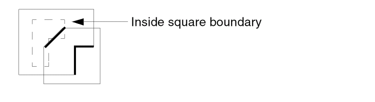
Use the following syntax for these options:
INT[S] layer1 layer2 LT n1 {CORNER-CORNER n2} {CORNER-EDGE n3}
Only 90 degree angles are treated as "CORNER".
(+) Flags inside segments of polygons of two layers that coincide.
(-) Does not flag violations on polygons that are part of the same node. Use the CONNECT command to establish nodal connectivity before using this option. This option checks only the data on the composite plane.
(-) Inverse of the U option. Flags violations on polygons that are part of the same node. Use the CONNECT command to connect nodes before using this option. Checks only data on the composite plane.
(+) Checks the inside edges of layer-a to the inside edges of all surrounding geometries of layer-b.
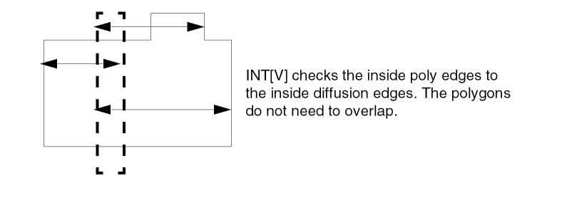
Checks the delta value in the x direction between two edges. The edges must project onto each other. Does not check non-Manhattan data.
Checks the delta value in the y direction between two edges. The edges must project onto each other. Does not check non-Manhattan data.
Layer Options
Checks the original layer, not the layer generated by the previous operation in the conjunctive rule. Use this option only with a conjunctive rule and on a layer with error flags.
Example 1
ENC layer1 layer2 LT 1 outl1 &
EXT layer1 layer3 LT 1 outl2 &
INT layer1[O] layer3 LT 2 OUTPUT err1 23
Example 2
INT srcdrn epi LT 4 OUTPUT drc04 31
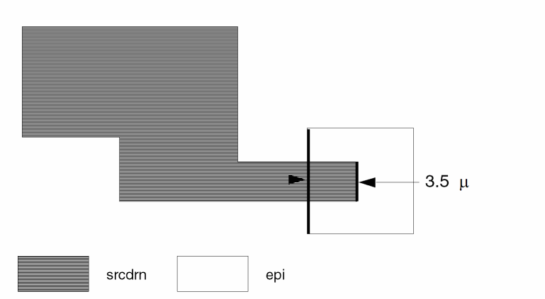
Example 3
This example checks the minimum intersection depth of poly and diffusion for forming capacitors. Touching is also an error.
INT[T] poly diff LT 2 OUTPUT drc04 32
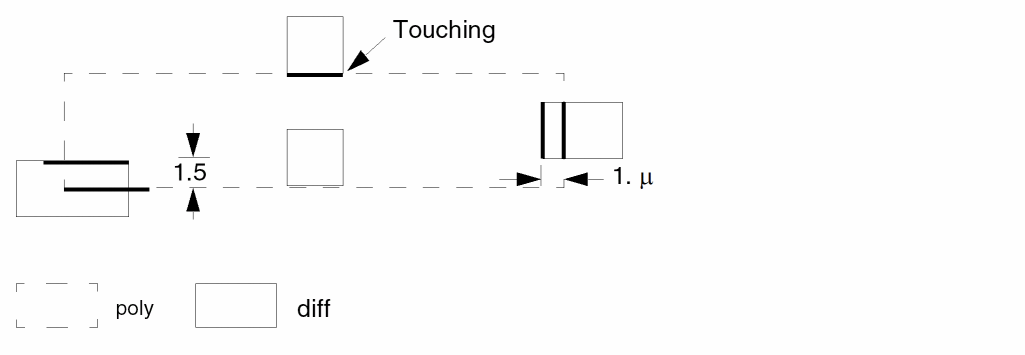
Example 4
This example checks for minimum width of metal at the region where metal overlaps the poly by less than 2 microns.
INT[P] poly metal LT 2 &
INT[P] metal metal[0] LT 6 OUTPUT drc04 33
Example 5
INT[P] poly metal&mpoly LT 2 &
INT[P] &mpoly metal LT 6 OUTPUT drc04 33
This example also checks for minimum width of metal at the region where metal overlaps the poly by less than 2 microns.
Layer metal is renamed to &mpoly in the conjunctive rename operation and now &mpoly contains the error flags from the joined operations. Also layer metal reverts to metal[O] at this point. The new layer &mpoly can be used in a later DRC check. The conjunctive rename is optional but can save CPU resources.
Example 6
This example checks for the minimum intersection depth of poly and metal, and depths that are less than 2 microns are output as errors. Errors generated by poly and metal and where poly and metal carry the same electrical node are not output as an error.
INT[N] poly metal LT 2 OUTPUT drc04 34
Example 7
INT[R] poly diff LT 4 cap
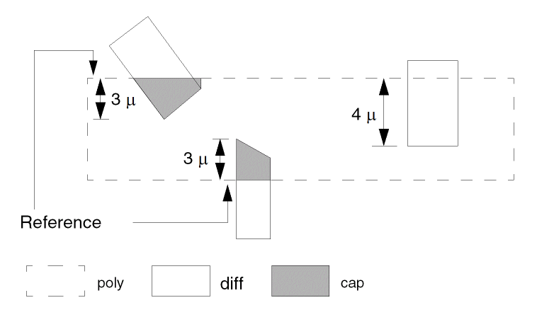
KEDTEXT
KEDTEXT = <kedtext_filename>
Description
Specify the text input source from a file for the "Keep Cell Text" feature in an LVS or LVL job. The format for the KEDTEXT file is the same as the HEDTEXT file.
There are two ways to specify text input source for the “Keep Cell Text” feature. One is the KTEXT command in the Input-Layer Block which reads texts from the CAD graphics database, the other is the KEDTEXT command in the Operation block which reads texts from a plain ASCII file. The two commands can exist simultaneously.
Checking Method
Arguments
Specifies the name of the file containing the text input source.
Example
KEDTEXT = myKedtext.txt
KEDTEXT = /mypath/myKedtext.txt
LCONNECT
LCONNECTlayerCONN/DISClabel{trapfile} OUTPUTc-name l-num{d-num}
Description
Determines if areas at specific layers are part of a labeled node. The command outputs the areas you specify to an output cell.
Arguments
The layer to check. The layer must be a conductor layer you define in the CONNECT-LAYER and CONNECT commands.
CONN means that the areas that are part of the labeled node are reported. DISC means that the areas that are not part of the labeled node are reported.
Text label of the node considered for the check. The label must be assigned text in the layout database and conform to the text rules.
Name you designate as the output file to contain composite trapezoids. Before you do any operation on a trapfile, you need to “OR” it.
Sends the results of the operation to an output cell. The output cell you specify cannot be used as the output of another command.
C-name is the name of the output cell and can have six alphanumeric characters or fewer and no special characters. L-num is the cell layer number determined by your CAD system.
If your c-name is rule03 and l-num is 5, the output cell name is rule0305.
Datatype number associated with the layer number (l-num) of the output cell. Use d-num for GDSII only; values can range from 0 to 63.
Examples
This example checks all polygons on the diffusion layer to see if any are disconnected to the labeled node VCC. The output is on layer 40 of cell difvcc40.
LCONNECT diff DISC vcc OUTPUT difvcc 40
This example checks all polygons on the pwell layer to see if any are disconnected to the labeled node VSS. The output is on layer 63 of cell flowel63.
LCONNECT pwell DISC vss OUTPUT flowel 63
LENGTH
LENGTHlayer-a{&layer-a1} GT/GE/ LT/LE/ RANGEn1{n2} {OUTPUTc-name l-num{d-num}} {&}
Description
Checks length dimensions. Use this check only as part of a conjunctive rule. When the dimensional check fails in the previous check, this command checks the dimension of the failure. It indicates a violation only when both checks fail.
Arguments
Renames (conjunctive rename) the layer containing the error flags. The original layer name is then restored to the original layer. No spaces are allowed between the layer-a and &layer-a1 names, for example, poly&rpoly.
Measures between all nonconsecutive pairs of inside edges of the polygons of the input layer. Flags violations after comparing the measurements against the limits you specify, including:
Sends the results of the operation to an output cell.
C-name is the name of the output cell and can have six alphanumeric characters or fewer and no special characters. L-num is the cell layer number determined by your CAD system. If your c-name is rule03 and l-num is 5, the output cell name is rule0305.
Format of the output is the same as the original database.
Datatype number associated with the layer number (l-num) of the output cell. Use d-num for GDSII only. Values can range from 0 to 63.
Example 1
EXT[P] metal LT 4 &
LENGTH metal GT 6 OUTPUT rule10 11
Example 2
This example checks for metal contact (contact) of internal size 3 by 3 only. Uses the conjunctive rename operation. Layer &cont3 can be used later in another conjunctive DRC check. Conjunctive rename is optional and can save CPU resources.
WIDTH contact LT 3 OUTPUT drc11 15
SIZE contact BY .2 ocont
ENC[P] contact&cont3 ocont RANGE 0.19 0.21 &
LENGTH &cont3 GT 3 OUTPUT drc11 17
Example 3
This example checks for poly overlap diffusion (gate extension) only on transistors having gate lengths 2 microns or less. Touching is also an error.
AND poly diff gate
ENC[T] gate diff LT .001 &
LENGTH gate LE 2 &
ENC[T] gate poly LT 2 OUTPUT drc11 12
LEXTRACT
LEXTRACTpset layer-a{layer-b} BY ELEMENT[type]{pfname}{&}
LEXTRACTpset layer-a{layer-b} BY PARASITIC[type]{pfname}{&}
LEXTRACT pset layer-a {layer-b} BY NODE {pfname} {&}
LEXTRACT[E] RES layer-c layer-d BY RES{[type]} &
Description
Extracts geometric parameters from one or two layers of a device (BJT, CAP, DIO, MOS, or RES). Specify parameters to extract in a PARSET command in the Description block. The number of input layers you specify with the LEXTRACT command depends on the primitive parameters you specify with the PARSET command. The first layer you specify must be a device layer or a layer with the device number tagged on by a DEVTAG command. The second layer you specify can augment the parameters you are extracting from the first layer.
When you use the LEXTRACT command, you must also specify a PARSET command in the Description block.
Group parameter extractions for each device type in a conjoined group. Specify only one LEXTRACT conjoined group with the EQUATION command for each device type. For a discussion of flexible LPE parameter set extraction, refer to Chapter 7, “Extracting Electrical Parameters (LPE).”
For bipolar devices, LEXTRACT extracts width and length, as well as the geometric parameters (area and perimeter) from one or more layers. Group all parameter extractions for each device type in a conjoined group. Specify only one conjoined group for each device type (element [type]).
Antenna Check
In certain applications, you might want to compare the ratio of device area to the layer area driving the devices. This check, called an antenna check, is useful when you want to ensure that induced capacitance, caused by a fabrication process or a circuit operation, does not cause the drive current or the transition time to become unstable. Use the NODE argument in the LEXTRACT command as part of an antenna check. Refer also to the CALCULATE, COMPUTE, and CHKPAR commands.
To perform antenna checks, you need to do the following:
- To form the necessary connection layers, use the layer operation.
- To extract the parameters per each node for specified layers, use the LEXTRACT BY NODE command.
- To calculate the parameter ration of each node among multiple layers, specify the CALCULATE command.
- To check and output the violation geometries, use the CHKPAR command.
To run an antenna check with HLPE
When running composite mode, COMPUTE reads the parameter file generated by the cell mode and add the data to the composite plane for each cell instance.
See Example 1 for an sample antenna check rule. For additional information about antenna checks, see “Writing Antenna Checks” in the “Writing Rules for Dracula” chapter of the Dracula User Guide.
When you use more than one LEXTRACT command, you need to group them together in the Dracula rules file. You cannot place another command within a group of LEXTRACT commands. In addition, you need to group LEXTRACT, DEVTAG, LVSCHK, or LPECHK commands together. Do not use any other command within any group of these commands.
Arguments
Name of the parameter set PARSET to extract (specified in the Description block). The name can have up to four alphanumeric characters, the first of which must be a letter.
The first layer from which parameters are extracted. This layer must be either the device layer or a layer with a device number tagged by the DEVTAG command.
The optional second layer from which parameters are extracted. It is used in relation to the first layer to extract geometric parameters such as overlapped areas and perimeters.
Extracts parameters from layer-a onto each node. Because of this, layer-a must contain nodal information. Use this keyword when checking the area ratio of layers on devices or long nodes (antenna check). For example:
LEXTRACT pset layer1 {layer 2} BY NODE outfile {&}
Type of device specified in the ELEMENT command. For example, BJT[NV] for a vertical npn and BJT[LP] for a lateral pnp. Also, the type of device specified in the PARASITIC command. Elements can be BJT, CAP, DIO, MOS, and RES. Parasitics can be CAP, DIO, and RES.
Output parameter file name. Specify only one file name for each conjoined group.
Conjunction of several extractions into one output file.
Example 1
The following is a sample rules file that checks connectivity up to metal1 for any antenna violation before processing metal2 and metal3.
*DESCRIPTION
PARSET ANT AREA PERI
*END
*INPUT-LAYER
NPLUS=1
NWELL=2
POLY=4
CONT=5
METAL=6 TEXT=20 ATTACH=METAL
PPLUS=7
VAPOX=8
VIA=9
METAL=10 TEXT=21 ATTACH=METAL
CONNECT-LAY= PWELL NWELL PDIFF NDIFF POLY METAL
SUBSTRATE CELLB = 12
*END
*OPERATION
NOT CELLB NWELL PWELL
NOT NPLUS POLY NDIFF
NOT PPLUS POLY PDIFF
OR PPLUS NPLUS PLUS
AND POLY PLUS GATE
AND PDIFF PWELL PPLUG
AND NDIFF NWELL NPLUG
CONNECT NDIFF NWELL BY NPLUG
CONNECT PDIFF PWELL BY PPLUG
CONNECT METAL NDIFF BY CONT
CONNECT METAL PDIFF BY CONT
CONNECT METAL POLY BY CONT
AND NDIFF CONT NCONT
AND PDIFF CONT PCONT

OR NCONT PCONT NPCONT
SELECT[N] METAL CUT NPCONT GMET
NOT METAL GMET M1     ; the concerned part

AND POLY CONT PLCONT
AND PLCONT GMET PGCONT
SELECT[N] POLY CUT PGCONT GPOL
NOT POLY GPOL NPOL
AND NPOL GATE NGPOL     ; the concerned part
NOT NPOL GATE NFPOL     ; the concerned part

LEXTRACT ANT NFPOL BY NODE AFPOLY
LEXTRACT ANT NGPOL BY NODE AGATE
LEXTRACT ANT M1 BY NODE PM1
CALCULATE RATIO= (SUM.AFPOLY+SUM.PM1)/SUM.AGATE
CHKPAR PAR RATIO NGPOL GT 100 LONG1 OUTPUT PLONG 50
CHKPAR PAR RATIO NFPOL GT 100 LONG2 OUTPUT PLONG 51
CHKPAR PAR RATIO M1 GT 100 LONG3 OUTPUT PLONG 52
*END
Example 2
*DESCRIPTION
PARSET pbip area peri ca cp ba bp ea ep
.
*END
*OPERATION
.
ELEMENT BJT[n]    emit   coll   base emit
DEVTAG BJT[n]     coll   collr
DEVTAG BJT[n]     base   baser
LEXTRACT pbip     emit   BY BJT[n] npar &
LEXTRACT pbip     collr  BY BJT[n] &
LEXTRACT pbip     baser  BY BJT[n]
Areas and perimeters of emitter, collector, and base are extracted and stored in the NPAR.DAT file. Because coll and base layers are not the device layer, they must be tagged with device numbers using the DEVTAG command. The device layer is emit. The above example handles npn devices with multiple emitters.
Example 3
Lateral PNP with multiple collectors:
*DESCRIPTION
PARSET plat area peri ca cp ba bp ea ep
.
*END
*OPERATION
.
ELEMENT BJT   [lp]    coll    coll   base   oemit
DEVTAG BJT    [lp]    oemit   emitl
DEVTAG[L]     emit l  emit    emitr
LEXTRACT      plat    emitr   BY     BJT[lp] bjt lp &
LEXTRACT      plat    coll    BY     BJT[lp]
BJT[LP] are lateral pnp bipolar transistors with multiple collectors around the same emitter. The oemit layer is true size emitter (emit) oversized so that it touches or overlaps the device layer (coll) to facilitate terminal extractions. Device numbers are tagged to the emit1 layer and then emit1 tags the emit layer and outputs to emitr. Areas and perimeters of emit and coll are extracted and put in the BJTLP.DAT file.
Example 4
Extracting width and length of a BJT:
*DESCRIPTION
 ...
MODEL=BJT[VN],VNPN BJT[LP],LPNP BJT[SP],SPNP DIO[OV],OVD
PARSET BJTS AREA OVPR L W
 ...
*END
*OPERATION
 ...
AND      EMIT BURIED     XYZ
NOT      XYZ  TRUBASE    MNO
EXT[PR]  VNPN CONT LT 6 DUMMY
ELEMENT    BJT[VN]  VNPN     BURIED   TRUBASE   METAL1
ELEMENT    BJT[LP]  CLPNP    CLPNP    BURIED    OLPNP
ELEMENT    BJT[SP]  SUBPNP   BULK     EMIT      TRUBASE
 ...
ELEMENT  RES  RESBODY  TRUBASE
PARAMETER RES 1
 ...
LEXTRACT BJTS VNPN DUMMY by BJT[VN] VNPARA &
EQUATION W=OVPR &
EQUATION L=AREA/W

LPECHK  BJTWPERCENT = 10.00 BJTLPERCENT = 11.0
LPECHK  RESWPERCENT =  5.00 RESLPERCENT =  8.0

*END
To extract the length and width of a BJT, you must define a PARSET with a W and L. Then specify an LEXTRACT defining the equations and extraction layers. In this example, an EXT[PR] check is done between the device layer and a contact layer to produce an intermediate layer that can compute the periphery overlap (OVPR). The periphery overlap is treated as W while L is computed from AREA divided by W. If no existing layer can be used together with the device layer to produce the overlap periphery you want, you might need to digitize a new layer for that purpose.
In the SPICE file generated by the LPESELECT BJT command in conjunction with the LEXTRACT command, the bipolar SPICE file has the following format:
CA = the area of the collector BP = the perimeter of the base
CP = the perimeter of the collector EA = the area of the emitter
BA = the area of the base EP = the perimeter of the emitter
Example 5
Q1 out1 in1 gnd npn $ CA=1050 CP=130 BA=500 BP=90 EA=100 EP=40
(Remember that $ is a SPICE comment character.)
Example 6
LEXTRACT ANT GATE BY NODE PGATE
LEXTRACT ANT NGATE BY NODE PNGATE
LEXTRACT ANT M1 BY NODE PM1
LEXTRACT ANT M2 BY NODE PM2
CALCULATE RES1 = PNGATE/PGATE
CALCULATE RES2 = (PNGATE + c1 * PM1)/PGATE
CALCULATE RES3 = (PNGATE + c1 * PM1 + c2 * PM2)/PGATE
CHKPAR PAR RES1 PGATE GT200 LONG1 OUTPUT PLONG 50
CHKPAR PAR RES2 PGATE GT300 LONG2 OUTPUT NLONG 50
CHKPAR PAR RES3 PGATE GT400 LONG3 OUTPUT LONG 50
This example is based on one parameter being extracted. For mixed calculations, use the following:
CALCULATE RES4 = (PNGATE.AREA + k1 * PM1.AREA + k2 * PM1.PERI)/PGATE.AREA
LEXTRACT[E] RES layer-c layer-d BY RES{[type]} &
Consider the rule fragment for extraction parameters of resistors with contacts (please see Figure 13-4 ).
;Element Definition
ELEMENT  RES{[type]} layer-a layer-b
;Tagging
DEVTAG           RES{[type]} layer-b layer-d
DEVTAG[L]        layer-d  layer-f   layer-c
; Resistor  Body parameter calculation, and ;;; Contact Resistor parameter calculation
LEXTRACT RES   layer-a     layer-b   BY RES{[type]}   pfname &
EQUATION      parameter_1 = FORTRAN-expression  &
EQUATION     parameter_2 = FORTRAN-expression    &
EQUATION      parameter_3 = FORTRAN-expression depends on
    parameter_1 and parameter_2   &
LEXTRACT  RES  layer-c  layer-d   BY RES{[type]}    &
EQUATION      parameter_4 = FORTRAN-expression  &
EQUATION      parameter_5 = parameter_3+ parameter_4
If layer-c is empty, parameter_4 is not calculated and parameter_5 is not calculated for this resistor (e.g. RES2 on Figure 13-4) either. To avoid this issue the [E] option is used. For instance, if you use:
LEXTRACT[E]  RES  layer-c  layer-d   BY RES{[type]}    &
EQUATION      parameter_4 = FORTRAN-expression  &
EQUATION      parameter_5 = parameter_3+ parameter_4
In this case, parameter_4 =0 for the empty layer-c case and
EQUATION parameter_5 = parameter_3+ parameter_4 (for RES1 and RES3)
EQUATION parameter_5 = parameter_3 (for RES2)
and all resistors are extracted.
Example 7
; Element Definition
ELEMENT          RES[D]   DRES       DRTRM
; Tagging
DEVTAG           RES[D]   DRTRM      TAGCON1
DEVTAG[L]        TAGCON1  DRTCON     DRCON
; Resistor Body parameter calculation, and ;;; Contact Resistor parameter calculation
LEXTRACT RES     DRES     DRTRM   BY RES[D]   pfname &
EQUATION      W=(W1+W2)/2 &
EQUATION      L=AREA/W &
EQUATION      RB=1000*L/W &
LEXTRACT[E] RES  DRCON    TAGCON1 BY RES[D] &
EQUATION      RC=2*25/(AREA/2) &
EQUATION      R=RB+RC
LINK
LINKlayerTOlabel
Description
Forces a layer with node information to a label (text). Use the LINK command after establishing the circuit connection. After a layer is linked, the original node information is overwritten. Use the LINK command only to connect the substrate layer when you cannot make a connection with the CONNECT command.
Arguments
Name of the layer of a previously generated layer or a layer name from the Input-Layer block.
Text label either from the CAD database text or from EDTEXT.
Example
LINK sub TO gnd
LPECHK
LPECHK {[options]} {SUBTYPE-AS-PARAM=YES/NO} {MOS-WIDTH-SUMMARY=YES/NO} {WPERCENT=n1} {LPERCENT=n2} {WEFFECT=n3} {CAPAREA=n4} {CAPVAL=n5} {DIOAREA=n6} {DIOPERI=n7} {RESSIZE=n8} {RESVAL=n9} {W/L-PERCENT=n10} {MULDELW=n11} {LISTUNMATCH=n12} {EAPER=n13} {PRINTLINE=n14} {BJTWPERCENT=n15} {BJTLPERCENT=n16} {RESWPERCENT=n17} {RESLPERCENT=n18}
Description
Specifies the LPE checking option. If you specify the SCHEMATIC command in the Description block, you can exercise LPE options on layout data and schematic data. The LPECHK and LVS options are similar in function. This command must fit on one line. To use multiple options, specify more than one LPECHK command.
If you specify LPECHK in your rule file, you must define the schematic file. Otherwise, you get an error message. If you do not have a schematic, Dracula interprets this as an error. Dracula ignores the command and generates a jxrun.com file. You must determine the seriousness of the error flagged by Dracula and whether you want to submit the job.
Arguments
Can include the following values:
|
Keeps parallel BJT transistors unsmashed, but smashes MOS, LDD, resistor, capacitor, and diode devices. |
|
|
Forms CMOS gates such as NORs, NANDs, AOIs, and OAIs, except when you specify the LPECHK |
|
|
Uses the information of body parameters to match parallel devices. LVSCHK uses the percentage tolerances described later (like WPERCENT, LPERCENT, CAPVAL, RESVAL, etc.) to match parallel transistors in the schematic with corresponding parallel transistors in the layout. For 4.8 or higher versions, this is the default. Otherwise, the default is to match pairs at random. |
|
|
Filters unused MOS devices (that is, for gate arrays). The FILTER-OPTIONS command overrides this option. |
|
|
Filters both the schematic and the layout in the same way. The FILTER-OPTIONS command overrides this option. |
|
|
Keeps parallel transistors “unsmashed.” Default is to smash devices. K overrides the B option. |
|
|
Same as the C option except AOI and OAI gates are not formed. The subtype restrictions still apply. L option overrides the C option. |
|
|
Forms parallel and series MOS structures even if neither is connected to power or ground. By default, LVS does not form SMID or PMID structures. This option enables LVS to recognize BiCMOS structures and enables the LVS gate level matching capability. You can use “O” option with any other option except the “X” option. |
|
|
Checks the ELEMENT capacitor’s polarity. This option does not swap the terminal order of the ELEMENT CAP and the CDL capacitor command. For addition information, refer to the ELEMENT CAP section in this chapter. See also the Z option in LPESELECT. |
|
|
Smashes MOS split-gates. The S-OPTION-CLASS command in the Description block determines whether this option smashes split gates connected to power or ground, split gates not connected to power or ground, or all split gates. The CARE-SPLIT-ORDER command in the Description block checks the input order of split gates. Device sizes (W and L) are combined using the usual formula for the related parallel devices. In cases where some of the input signals to the series structures are swapped, the MOS devices on one series structure are mapped to the MOS devices on the other series structure at random for the purpose of combining device sizes. Intermediate nodes of the series structures are also combined as a single node for the resulting single series structure. Parasitics (diodes, capacitors) for these nodes are lumped together. |
|
|
Considers substrate terminal connections as regular terminal connections during matching process. The matching process propagates the match information through the substrate connections and the subsequent instances. |
|
|
Reports in the discrepancy file (.LVS) only the unmatched schematic and unmatched layout devices on matched nodes (Type 4, 5, and 6 LVS errors). Device size, substrate, and subtype checks are not affected. |
|
|
Compares layout to schematic on the transistor level instead of on the logic-gate level. |
If you specify YES, Dracula matches two devices with different subtypes. Dracula then checks the subtype as if it were checking a parameter.
If you specify NO, and the two devices have different subtypes, Dracula treats them as different devices and never matches them. Default is NO.
If you specify YES, Dracula reports the summary of MOS devices by subtype and width in the .lvs file.
If you specify NO, Dracula uses the default report format.
Percentage of the transistor width tolerance when compared with the schematic width specification (0 < n1 < 100; the default is no check).
Percentage of the transistor length tolerance when compared with the schematic length specification (0< n2 < 100; the default is no check).
A user-specified value, the effective MOS channel width/length calculation. You can specify WEFFECT as a positive or negative value. Each 15-degree turn in a transistor channel causes a 1/6 fraction of WEFFECT specified times length (L) to be added or subtracted from a transistor default width (W) for a pull down device (default is 0). For a load-device, W remains as is and L is modified. See the algorithm at the end of this option list.
Percentage tolerance of the capacitor area in the LVS comparing process (0 < n4 < 100; the default is no check). See CAPVAL option.
Percentage tolerance of the capacitor value in the LVS comparing process (0 < n5 < 100; the default is no check). You can specify only CAPAREA or CAPVAL, but not both; the choice depends on the SPICE or CDL netlist specification.
Percentage tolerance of the diode area in the LVS comparing process (0 < n6 < 100; the default is no check).
Percentage tolerance of the diode periphery in the LVS comparing process (0 < n7 < 100; the default is no check).
Percentage tolerance of the number of squares in a resistor in the LVS comparing process (0 < n8 < 100; the default is no check). See also the RESVAL option.
Percentage tolerance of resistor value in the LVS comparing process (0 < n9 < 100; the default is no check.). You can specify only RESSIZE or RESVAL, but not both, and the choice depends on the SPICE/CDL netlist specification. For additional discussion and illustrations, refer to Chapter 7, “Extracting Electrical Parameters (LPE).”
Percentage tolerance of MOS transistor width/length in the LVS comparing process (0 < n10 < 100; the default is no check).
User-specified value compensating for multiple parallel finger MOS transistors on effective channel widths. MULDELW is usually a negative value (default is 0). For more information about parallel MOS transistors, refer to Chapter 6, “Comparing Layouts and Schematics (LVS).”
Maximum number of unmatched schematic and layout devices to print out. (0 ≤ n12 ≤ 1,000,000; the default is 100).
Percentage tolerance of the bipolar emitter area in the LVS comparison (0 < n13 < 100;the default is no check). You must input emitter sizes of bipolar transistors from the schematic netlist onto the schematics.
Maximum unmatched occurrences to print out. (0 < n14 < 1,000,000; the default is 1,000).
Percentage tolerance of the BJT transistor width in the LVS comparing process. (0 < n15 < 100; the default is no check).
Percentage tolerance of the BJT transistor length in the LVS comparing process (0 < n16 < 100; the default is no check).
Percentage tolerance of the resistor width in the LVS comparing process (0 < n17 < 100; the default is no check). Both length and width must be specified if the option for smashing parallel resistors is on. The default is smash parallel resistors.
Percentage tolerance of the resistor length in the LVS comparing process (0 < n18 < 100; the default is no check). Both length and width must be specified if the option for smashing parallel resistors in on. The default is smash parallel resistors.
The following algorithm is used:
For WEFFECT = 0, Wactual = W Lactual = A/W
-
For a pulldown device (L is unmodified)
W{actual} = W{init} - (WEFFECT * I *L) ; if W{init} is greater than L
where
W{actual} = the actual width of the gate
W{init} = the initial width of the gate. This is always calculated by Dracula.
WEFFECT = a compensation coefficient you supply to Dracula to correctly calculate the actual width/length of a transistor gate.
I = the total of a device’s internal angles (in units of 90 degrees)
L = the length of the gate which is equal to the total area of the gate divided by the initial width of the gate (e.g. Area/W{init}) -
For a load device (W is unmodified)
L{actual} = L{init} - (WEFFECT * I *L) ; if L{init} ≥ W
where
L{actual} = the actual length of the gate
L{init} = the length of the gate which is equal to the total area of the gate divided by the width of the gate (e.g. Area/W)
WEFFECT = a compensation coefficient you supply to Dracula to correctly calculate the actual width/length of a transistor gate.
I = the total of a device's internal angles (in units of 90 degrees, with each internal angle rounded to the nearest 15 degrees)
W = the width of the gate. This is always calculated for you by Dracula.
For additional discussion and illustrations, refer to Chapter 7, “Extracting Electrical Parameters (LPE).”
Example 1
LPECHK[X] WPERCENT = 15 LPERCENT = 15
Example 2
I/90 = 2 [90 + 90 = 180 degrees]
For a pulldown device: WEFFECT= 0.5, W = 12 L = 1, and Wactual = 11
For a load device: WEFFECT= 0.5, W = 1 L = 12, and Lactual = 11
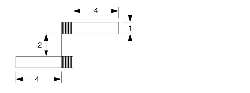
Example 3
I/90 = 1 [45 + 45 = 90 degrees]
For a pulldown device: WEFFECT = 0.0, W = 16 L = 3.31, and Wactual = 16 where WEFFECT = CORNER.
For another pulldown device: WEFFECT = 1.0, W = 16 L = 3.31, and Wactual = 12.69
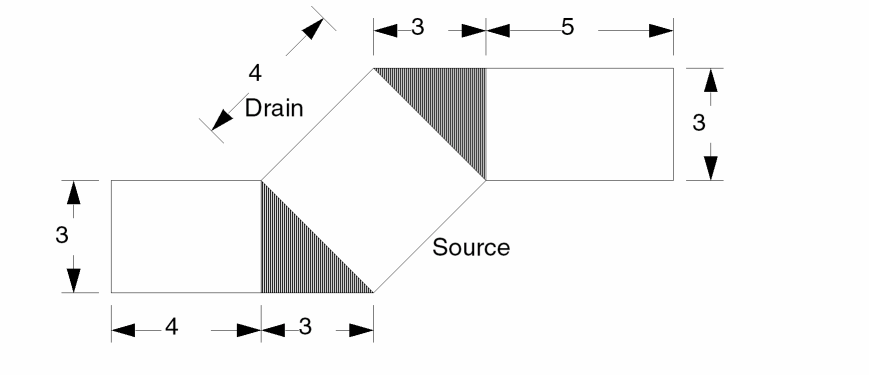
LPESELECT
LPESELECT {[options]} element {[type]} {GE/GT val-a} {RANGE val-a val-b} {CORNER = n1} {OUTPUT c-name {l-num}} {&}
Description
Selects a group of elements to print in CDL or SPICE format. You can use more than one LPESELECT command to put more than one group of elements on the same report. You can select only parasitic capacitance when you specify your own thresholds.
LPESELECT and PRE
With PRE, the LPESELECT RES command indicates that the parasitic resistor elements should be output to a SPICE or CDL netlist for PARASITIC RES. It also short circuits nodes connected to parasitic resistors whose resistance is under a specified threshold. The other LPESELECT element options (MOS, DIO, CAP, and BJT) report the shorted nodes as a single node.
The S (backannotation) option indicates that the nodes in the output file are labeled with the node names derived from the LVS check netlist used during the first connection pass. Subnodes (split nodes) are labeled with names derived from the schematic netlist, for backannotation, or derived from the node numbers obtained in the first pass, when backannotation is not specified. To get the actual subnode names, the node name or the node number is concatenated with a delimiter and a subnode number. The delimiter is a colon (:) or the delimiter specified in the PRE command SUBNODE-DELIMITER in the Description block.
For layout-only jobs (where there is no backannotation), the prefix of parasitic resistance, capacitance, and diode are RR, CC, and DD, respectively. To specify a different parasitic prefix, see the PREFIX-PARASITIC section in Chapter 11 of this manual.
Arguments
|
Flags capacitances on all nodes, including power and ground nodes. If you do not specify this option, LPESELECT does not report capacitances on power and ground nodes. |
|
|
Checks cross-coupling capacitance. If you do not specify cross-coupling capacitance, total loading is assumed. Use this option with the S option when you want to group or smash different subtypes of capacitors. Option C overwrites option A and filters out power to group parasitic capacitances. |
|
|
When used with the S option, specifies that the device number assigned by LOGLVS is reported in the output SPICE file. The corresponding device name and number is stored in EXPELE.LIS in ASCII format, which is generated by LOGLVS. |
|
|
Suppresses the output “/” between the SUBCKT I/O pins and names in the HLPE or HPRE extracted reports. In Dracula 4.81 and subsequent versions, you can now apply this E option to box elements too. When this E option is turned on, the “/” between I/O pins and a box element’s boxname in SPICE output is suppressed. See “Example 6 - Example For The E Option” for more information. |
|
|
Specifies that original ground node names, rather than the default VSS node name, are used in the output SPICE file. This option should not be used with the N option. VSS is the default for composite and cell mode. In multiple-ground cases, if you want only one of them as ground node in the output SPICE file, the LPE-GROUND command now lets you specify a unique ground name. The LPE-GROUND command overwrites this LPESELECT[G] command. |
|
|
Reports the capacitance, area and perimeter of capacitors. The area and the perimeter are reported as a comment with the prefix |
|
|
Specifies that parallel transistors, transistors of the same source, gate, and drain (connected to the same nodes) do not smash into one. Instead, LPESELECT reports these transistors individually. For a layout-only job, it can be used to turn off the smash of the BJT elements. This option also specifies that parallel boxes are not smashed into one. |
|
|
Disallows pin swapping that might result from backannotating a SPICE file based on the schematic. Use this option with the S option when you want to backannotate a SPICE file based on the layout with no pin swapping. For a layout-only job, use this option to retain the terminal order of CAP elements. |
|
|
Specifies to keep the original instance and device names of HLPE/HPRE or CELL mode LPE extracted results instead of renaming the extracted results Xnnn. |
|
|
Checks cross-coupling capacitance as a percentage of total loading. If you do not specify cross-coupling capacitance, this command performs a check directly against val-a. Options C, P, and A are implemented only to select CAP (capacitors). |
|
|
Reports the area and perimeter of parasitic capacitors. Reports the area in place of the capacitance value. Reports the perimeter as a comment with the prefix “PERI=.” |
|
|
Schematic node names report preferred (from LOGLVS). For this S option, the schematic ground is used in flat mode. VSS is still used as the default for composite and cell mode. You can use the G option or LPE-GROUND to overwrite the default ground VSS. |
|
|
This option works with the ‘S’ option. Using this option presents the pin order in the report as it is found in the netlist .SUBCKT statement. |
|
|
Outputs cross-coupling capacitance and does not filter out parasitics between multiple power or ground busses (for example, analog to digital power busses). Parasitic capacitance with both nodes at a power or ground node is not filtered out. Option T is a superset of option C and cannot be used with A or C. |
|
|
Does not comment out parasitic CAP and RES whose terminals are connected to power and ground nodes or power and ground subnodes in the SPICE output. This option takes effect whether back annotation is on or off. |
|
|
Specifies the expanded name of cell instances without the prefix X. |
|
|
Reports L (length) and W (width) of bipolar transistor (BJT) devices and resistance. In the Dracula versions prior to 4.81, this W option supported the L/W of only resistors. In Dracula 4.81 and subsequent versions, this W option in the LPESELECT command supports the L/W of not just resistors, but also the L/W (width) of bipolar transistor (BJT) devices on LVS and prints that W/L into SPICE netlists. For example, LPESELECT[W] BJT
For BJT devices, Dracula needs to specify this L/W using the LEXTRACT command in your rule file.
|
|
|
Does not print out commented devices and cell instances. If you do not specify this option, Dracula outputs commented devices and cell instances. |
|
|
Reports the x/y location of all element types in the LPESELECT listing file. |
|
|
Checks the ELEMENT capacitor polarity. This option does not swap the terminal order of the ELEMENT CAP and the CDL capacitor command. This is a new option for LPESELECT in Dracula 4.81 and functions the same way as the P option on LPECHK or LVSCHK. By default, the Dracula tool smashes parallel devices in LVS and LPE operations. But, you can prevent the smashing of capacitors with different polarity by using the [P] option of the LPECHK or LVSCHK commands. When there is just the LPESELECT command in the rule file (and you are not using LPECHK or LVSCHK commands), you need to prevent the smashing of capacitors with different polarity. In such a case, the Z option of the LPESELECT command helps you check the polarity of capacitors. If in the rule file, the LPECHK or LVSCHK exists with LPESELECT[Z], PDRACULA produces the following warning messages (depending on the commands that you are using):
The [Z] option takes the CAP element type only. When using with other elements, PDRACULA produces the following WARNING message
LPESELECT[Z] option is valid for CAP element only
See “Example 7 - First Example With the Z option in LPESELECT” and |
One of the device types listed below. If you do not include element, LPESELECT selects all device types.
For more information about ELEMENT MOS/BJT/RES, refer to Chapter 7, “Extracting Electrical Parameters (LPE).”
The type code you specify in the element device command. If you do not specify a type, this command invokes all element types.
To group or smash different subtypes of capacitors, specify type as [new-subtype:subtype+subtype+...]. This syntax sums the capacitance values of multiple subtypes into a new subtype. The SPICE output file then contains all parasitic metal caps, all poly capacitors, and so forth, smashed into a new group subtype. The subtypes can have different parset numbers and must be defined by PARASITIC commands.
The GE and GT options work for parasitic devices only.
If you do not specify this field during a conjunct, the default relational condition is GE 0.
Element parameters, which must be greater than or equal to val-a, and less than or equal to val-b.
Specifies value-a or value-b, which can be a floating point number (maximum of seven digits) or a floating-point number followed by an integer exponent (maximum two digits). When you specify floating-point numbers, the leading zeros are not counted in the seven-character restriction. The preprocessor rounds the value at the seventh digit. In scientific notation, the limit is 16 characters truncated at the 17th character.
The effective MOS channel width/length calculation. You can specify CORNER as a positive or negative value. For a pulldown device (default = 0), for each 15-degree turn in a transistor channel, a 1/6 fraction of CORNER specified times length (L) is added or subtracted from a transistor default width (W). For a load-device, W is not changed and L is modified.
CORNER uses the same algorithm as WEFFECT in LPECHK.
Outputs SPICE listing to a file.
C-name and l-num are concatenated to make up the file name and the subcircuit name of the SPICE listing. C-name can have six alphanumeric characters. If l-num is not specified, only c-name is used. For example, if c-name = CKTNAM and l-num = 10, the output file name is CKTNAM10 and the subcircuit name is the same in the SPICE listing.
Indicates a conjunctive rule. You can join LPESELECT only with other LPESELECT commands.
Example 1
This example shows how you can obtain layout node number information.
LPESELECT mos &
LPESELECT dio &
LPESELECT cap GE 0.01 OUTPUT cktnam 10
Example 2
This example uses the S option to obtain schematic node name information. This example assumes a SCHEMATIC is provided and the LPECHK command is invoked.
LPECHK
LPESELECT [SY] MOS[N] CORNER = 0.5 &
LPESELECT [SY] MOS[P] CORNER = 0.5 &
LPESELECT[S] DIO[N] &
LPESELECT[S] DIO[P] &
LPESELECT[S] CAP[A] GT 0.0 &
LPESELECT[S] CAP[B] GT 0.0 &
LPESELECT[S] CAP[C] GT 0.0 OUTPUT testck
The output file name is testck.dat. It contains listings of the following:
- MOS type N and type P are grouped separately with their effective transistor sizes calculated and their x/y coordinates indicated.
- DIODE type N and type P are grouped separately.
- Parasitic capacitor types A, B, and C are grouped separately.
Example 3
In the following example, parasitic capacitor types A, B, C are grouped as a new group subtype D.
LPESELECT[CS] CAP[D:A+B+C] GT 0
Example 4
LPESELECT[SO] MOS &
LPESELECT[S] CAP[A] GT 0.0 OUTPUT SPICE
Example 5
LPESELECT[S] RES GE 500 &
LPESELECT[S] MOS &
LPESELECT[S] DIO &
LPESELECT[S] CAP OUTPUT SPICE
Any parasitic resistors with values under 500 are shorted. Units are specified in the command under the Description block.
Example 6 - Example For The E Option
LPESELECT[E] IND OUTPUT SPICE
XB1009 5 OUT IND NR=2.50 W=15.00U S=1.50U RAD=60.00
XB1010 18 20 IND NR=4.50 W=15.00U S=1.50U RAD=30.00
======
|
---> pin list
Without the E option, the output would be as follows:
XB1009 5 OUT / IND NR=2.50 W=15.00U S=1.50U RAD=60.00
XB1010 18 20 / IND NR=4.50 W=15.00U S=1.50U RAD=30.00
Example 7 - First Example With the Z option in LPESELECT
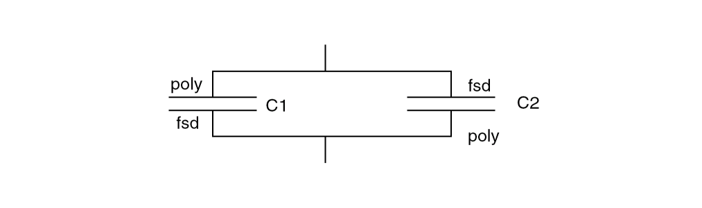
LPESELECT CAP OUTPUT SPICE
LPESELECT CAP[A] GT 0.0 OUTPUT SPICE
C1 and C2 capacitors are smashed. Dracula produces SPICE parameters of smashed capacitors C1+C2.
LPESELECT[Z] CAP OUTPUT SPICE
LPESELECT[Z] CAP[A] GT 0.0 OUTPUT SPICE
LPECHK[P] ... LPESELECT CAP OUTPUT SPICE
LPECHK[P] ... LPESELECT CAP[A] GT 0.0 OUTPUT SPICE
LVSCHK[P] ...LPESELECT CAP OUTPUT SPICE
LVSCHK[P] ...LPESELECT CAP[A] GT 0.0 OUTPUT SPICE
C1 and C2 capacitors are not smashed. Dracula produce SPICE parameters of C1 and C2 capacitors separately.
Example 8 - Second Example With the Z option in LPESELECT
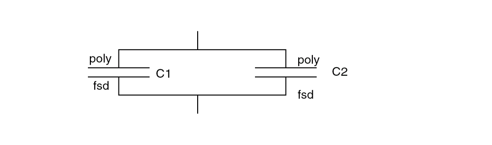
C1 and C2 capacitors are smashed. Dracula produces SPICE parameters of smashed capacitors C1+C2
These options, the LPESELECT [Z] option, the LPECHK [P] option, and the LVSCHK[P] have no effect on smashing.
LVSCHK
LVSCHK {[options]} {SUBTYPE-AS-PARAM=YES/NO/BCDLMR} {MOS-WIDTH-SUMMARY=YES/NO} {MOSCAP-AREA = n0}{PRINTLINE = n1} {WPERCENT = n2} {LPERCENT = n3} {WEFFECT = n4} {CAPAREA=n5} {CAPVAL=n6} {DIOAREA=n7} {DIOPERI=n8} {RESSIZE=n9} {RESVAL=n10} {W/L-PERCENT=n11} {MULDELW=n12} {LISTUNMATCH=n13} {EAPER=n14} {BJTWPERCENT=n15} {BJTLPERCENT=n16} {RESWPERCENT=n17} {RESLPERCENT=n18} {LDDWEFFECT=n19} {SMASH=[CDMRQ}]
Description
Extracts the layout database for a consistency check between layout and schematic. This command must fit on one line. To use multiple options, specify more than one LVSCHK command.
If you specify LVSCHK in your rule file, you must define the schematic file. Otherwise, you get an error message. If you do not have a schematic, Dracula interprets this as an error. Dracula ignores the command and generates a jxrun.com file. You must determine the seriousness of the error flagged by Dracula and whether you want to submit the job.
The DRAC_MAX_AMB_PARA_GRP variable can be set as the node count limit for ambiguous group matching. The default limit is 1000. A value less than or equal to zero will switch off the algorithm completely. If the variable is set, the following message will appear:
*/L* USING ENV. VARIABLE DRAC_MAX_AMB_PARA_GRP= n.
Arguments
|
Keeps parallel BJT transistors unsmashed, but smashes MOS, LDD, resistor, capacitor, and diode devices. |
|
|
Forms CMOS gates such as NORs, NANDs, AOIs, and OAIs except when you specify the LVSCHK
|
|
|
Controls the matching of parallel devices. For ambiguous groups of devices, Dracula has to determine which schematic should match layout. E is a scheme to start from the device and E’ is scheme to start from the node. It is best to run LVSCHK twice, once with E and once with E’, (or in reverse sequence) then compare the results. Only real errors will appear in both runs. E and E’ use the percentage tolerances described later (for example, WPERCENT, LPERCENT, CAPVAL, RESVAL, and so on) to match parallel devices in the schematic with corresponding parallel devices in the layout based on the information of body parameters.
|
|
|
Filters the unused MOS devices, for example, gate arrays. Allows the layout and schematic to be filtered differently. The FILTER-OPTIONS command overrides this option. |
|
|
Filters both the schematic and the layout in the same way. The FILTER-OPTIONS command overrides this option. |
|
|
Merges all SUP and SDW serial MOS devices with a common gate and a common substrate into a single MOS device. If WPERCENT is specified then all MOS devices must have a same width. The width will be written onto a single merged MOS device. The length value will be equal to the sum of the length of all merged MOS devices. If MOS devices do not have equal width then the devices are not merged. |
|
|
Merges all SMID serial MOS devices with a common gate and a common substrate into a single MOS device. If WPERCENT is specified then all MOS devices must have a same width. The width will be written onto a single merged MOS device. The length value will be equal to the sum of the length of all merged MOS devices. If MOS devices do not have equal width then the devices are not merged. |
|
|
Keeps parallel devices “unsmashed.” Default is to smash devices. The K option overrides the B option. In Dracula 4.81 and subsequent versions, a qualifier has been added to the K option such that it will not smash parallel devices with the exception of those devices you specify in the qualifier.
When the S and K options are turned on at the same time, the S option will outweigh the K option, which means that the K option will have no effect and PDRACULA will output warning message to notify users of this conflict situation. However, the |
|
|
Same as the C option except does not form AOI and OAI gates. Subtype restrictions still apply. L option overrides the C option. |
|
|
Dracula recognizes inverters when the inverter has been created by shorting the gates of a NAND or a NOR structure together. |
|
|
Check gate level substrate terminal connections. Without this option, only transistor level substrate connections are considered as regular terminals during the matching process if |
|
|
Forms parallel and series MOS structures even if neither is connected to power or ground. By default, LVS does not form SMID or PMID structures. This option enables LVS to recognize BiCMOS structures and enables the LVS gate-level matching capability. You can use the O option with any other option except the X option. |
|
|
Checks the ELEMENT capacitor’s polarity. This option does not swap the terminal order of the ELEMENT CAP and the CDL capacitor command. See the ELEMENT CAP command for additional information. See also the Z option in LPESELECT. |
|
|
Smashes MOS split-gates. The S-OPTION-CLASS command in the Description block determines whether this option smashes split gates connected to power or ground, split gates not connected to power or ground, or all split gates. The CARE-SPLIT-ORDER command in the Description block checks the input order of split gates. This illustration shows a split gate SUPI device smashed to a single SUP device. This is how the S option works by default. 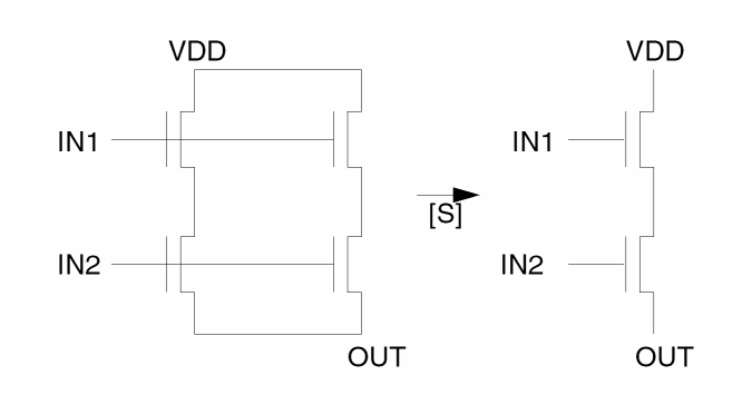 |
|
|
Considers substrate terminal connections as regular terminal connections during the matching process. The matching process propagates the match information through the substrate connections and the subsequent instances. This option cannot trace the substrate nodes of pseudo-gate structures. To match the substrate, do not form a pseudo-gate. |
|
|
Reports in the discrepancy file (.LVS) only the unmatched schematic and unmatched layout devices on matched nodes (Type 4, 5, and 6 LVS errors). Device size, substrate, and subtype checks are not affected. |
|
|
Carries out the comparison at the transistor level (that is, no swap allowed). |
|
|
Filters out devices with no general paths to any nonpower/ground pad. |
SUBTYPE-AS-PARAM=YES/NO /BCDLMR/X
Determines whether Dracula matches devices with subtypes and treats the subtypes as parameters.
If you specify YES, Dracula matches all devices with different subtypes. Dracula then checks the subtypes as if it were checking parameters.
If you specify NO, and the MOS, LDD, and BJT devices have different subtypes, Dracula treats them as different devices and does not match them with subtypes. However, Dracula matches all other devices, such as RES, CAP, and DIO, with subtypes and treats the subtypes as parameters, as if SUBTYPE-AS-PARAM were set to YES. The default is NO.
If you specify B, C, D, L, M, or R, Dracula treats the subtypes of the specified devices as parameters. The devices that you can specify are the following:
For example, SUBTYPE-AS-PARAM=BD causes Dracula to treat only the subtypes of BJTs and diodes as parameters.
If you specify X, Dracula does not match any device subtype as a parameter.
If you specify YES, Dracula reports the summary of MOS devices by subtype and width in the .lvs file.
If you specify NO, Dracula uses the default report format.
Checks the capacitance effect in a MOSCAP device area. Because a MOSCAP device has characteristics similar to a capacitor, this check measures the capacitance effect. By default, Dracula checks only the width and length of a MOSCAP. With this option turned on, if the W/L values do not match, the area is checked for a capacitance effect. If this option is not turned on, Dracula verifies a MOSCAP device as a MOS device. It does not measure the capacitance effect of other types of devices.
The maximum unmatched occurrences to print out (0 < n1 < 1,000,000; default =1,000).
The percentage tolerance of the MOS transistor width in the LVS comparing process (0 < n2 < 100; default = no check).
The percentage tolerance of the MOS transistor length in the LVS comparing process (0 < n3 < 100; default = no check).
Effective MOS channel width/length calculation you specify. You can specify WEFFECT as a positive or negative value. Each 15 degree turn in a transistor channel causes a 1/6 fraction of WEFFECT specified times length (L) to be added or subtracted from a transistor default width (W) for a pull-down device (default = 0). For a load-device, W remains as is and L is modified.
The following algorithm is used:
For WEFFECT = 0, Wactual = W Lactual = A/W
For additional discussion and illustrations, see Chapter 7, “Extracting Electrical Parameters (LPE).”
Percentage tolerance of the capacitor area in the LVS comparing process (0 < n5 < 100; the default is no check.). See CAPVAL option.
Percentage tolerance of the capacitor value in the LVS comparing process (0 < n6 < 100; the default is no check.). Only CAPAREA or CAPVAL can be specified, but not both, and the choice depends on the SPICE/CDL netlist specification.
Percentage tolerance of the diode area in the LVS comparing process (0 < n7 < 100; the default is no check).
Percentage tolerance of the diode periphery in the LVS comparing process (0 < n8 < 100; the default is no check).
Percentage tolerance of the number of squares in a resistor in the LVS comparing process (0 < n9 < 100; the default is no check). See RESVAL option. *.RESSIZE doesn’t compare the width/length of resistors. It allows these values to be put into the LVSLOGIC.DAT file from the input CDL/Spice netlist.
Percentage tolerance of resistor value in the LVS comparing process (0 < n10 < 100; the default is no check). You can specify only RESSIZE or RESVAL, but not both, and the choice depends on the SPICE/CDL netlist specification. For additional discussion and illustrations, see Chapter 7, “Extracting Electrical Parameters.” *.RESVAL allows the resistance values to be put into the LVSLOGIC.DAT file from the netlist.
|
When using LOGLVS it is necessary to specify either
*.RESVAL or *.RESSIZE, but not both in the CDL/Spice file. (This is already mentioned in Chapter 5, under the *.BIPOLAR section. Similarly you can specify either *.CAPVAL or *.CAPAREA, but not both in the CDL/Spice file). |
|
If you are running CDLOUT to generate the CDL netlist make sure that you have properly set the values for the Check Resistors and Check Capacitors fields in the form to have the appropriate parameter information sent to the netlist file for resistors and/or capacitors respectively. |
|
In a typical resistor CDL card, you have the following fields: |
|
|
|
If you want to check the resistor’s value, put the value of this resistor in the |
|
If you want to check the resistor’s size (number of squares), put the number of squares of the resistor in the |
|
The |
Percentage tolerance of the MOS transistor width/length in the LVS comparing process (0 < n11 < 100; the default is no check).
Value you specify compensating for multiple parallel finger MOS transistors on effective channel widths. MULDELW is usually a negative value. The default is 0. For information about parallel MOS transistors, refer to Chapter 6, “Comparing Layouts and Schematics (LVS).”
Maximum number of unmatched schematic and layout devices to print out (0 ≤ n13 ≤ 1,000,000; the default is 100).
Percentage tolerance of the bipolar emitter area in the LVS comparison (0 < n14 < 100; the default is no check). You must input emitter sizes of bipolar transistors from the schematic netlist onto the schematics.
Percentage tolerance of the BJT transistor width in the LVS comparing process (0 < n15 < 100; the default is no check).
Percentage tolerance of the BJT transistor length in the LVS comparing process (0 < n16 < 100; the default is no check).
Percentage tolerance of the resistor width in the LVS comparing process (0 < n17 < 100; the default is no check). Both length and width must be specified if the option for smashing parallel resistors is on. The default is smash parallel resistors. If either length or width is not specified, all width/length of resistors are 0, which means unspecified.
Percentage tolerance of the resistor length in the LVS comparing process (0 < n18 < 100; the default is no check). Both length and width must be specified if the option for smashing parallel resistors is on. The default is smash parallel resistors.
Add this argument, LDDWEFFECT for effective LDD channel width/length calculation. Same usage as WEFFECT (see the WEFFECT argument above) except that LDDWEFFECT is for LDD calculation whereas WEFFECT is for MOS calculation.
LVSCHK LDDWEFFECT = 1.0
Add this argument to set or clear bytes. When LVSCHK[SK] is used, S overrides K, and thus all CDMRQ gets cleared. When you use the syntax
C = capacitors D = diodes M = MOS transistors R = resistors Q = BJT bipolar devices
If you use the K option and specify any of the above devices in the SMASH qualifier all devices with the exception of those listed in the qualifier will not be smashed.
See the “Example 2 - Using the K option and the SMASH Qualifier” in this section for more information.
Examples
Example 1
LVSCHK[FX] PRINTLINE = 3000
Checks a gate array circuit at its transistor level. The printout lists up to 3,000 unmatched occurrences. The device width and length are not checked. W and L are compared only when WPERCENT and LPERCENT are mentioned.
LVSCHK[S] WPERCENT = 10 LPERCENT = 5 WEFFECT = .5
Checks a circuit with pseudo gates being formed. All split-gates in the schematic and layout are smashed to a single SUP or SDW device for LVS checking. MOS transistor width and length are checked to ±10% and ±5%, respectively. LVS calculates the device’s W and L values as before and only modifies the device’s W value according to the formula above for a pull-down device. For every 90-degree turn and every 45-degree turn, W is reduced (subtracted) by (.5)*(L) and (.25)*(L), respectively. The L value remains the same. If a load device is encountered, L is modified and the W value remains the same.
LVSCHK WPERCENT=5 LPERCENT=2 RESVAL=5 DIOAREA=10
LVSCHK DIOPERI=10 CAPVAL=5
This compares layout database device sizes to the netlist device sizes. Comparison of MOS width is at 5%, MOS length at 2%, resistor values at 5%, diode area at 10%, diode perimeter at 10%, and capacitor value at 5%. You can repeat the LVSCHK command to include the desired check options, and their tolerances are +/-. To compare resistor, diode, and capacitor values, the appropriate options must be turned on in the input SPICE/CDL netlists.
LVSCHK[P] W/L-PERCENT=1 LISTUNMATCH=500
This compares the layout database device size W/L ratios to the netlist device size W/L ratios. Comparison of MOS W/L ratios is at 1%. The capacitor polarity is checked such that ELEMENT CAP terminals are not allowed to swap with the CDL capacitor terminals. The printout lists up to 500 unmatched schematic and layout devices.
To do device size checks of CAP and RES, specify the ELEMENT CAP and ELEMENT RES commands along with the PARAMETER CAP and PARAMETER RES commands. There is no PARAMETER DIO command.
I/90 = 2 [90 + 90 = 180 degrees]
For a pulldown device: WEFFECT= 0.5, W = 12 L = 1, and Wactual = 11
For a load device: WEFFECT= 0.5, W = 1 L = 12, and Lactual = 11
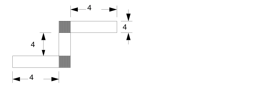
I/90 = 1 [45 + 45 = 90 degrees]
For a pulldown device: WEFFECT = 0.0, W = 16 L = 3.31, and Wactual = 16 where WEFFECT = CORNER.
For another pulldown device: WEFFECT = 1.0, W = 16 L = 3.31, and Wactual = 12.69
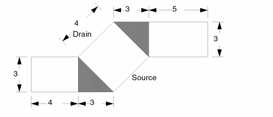
Example 2 - Using the K option and the SMASH Qualifier
LVSCHK[K] SMASH=[RC]
The above command will not smash any parallel devices with the exception of parallel resistors and capacitors. If you use the above command in the OPERATION block and SMASH-RES-TYP = YES and/or SMASH-CAP-TYP=YES command in the DESCRIPTION block of commands, this command will only smash series devices.
Example 3 - Merging SUP and SDW Devices into a Single MOS
LVSCHK[H]
This example merges all SUP and SDW serial MOS devices with a common gate into a single MOS device, but it does not merge SMID MOS devices with a common gate:
Example 4 - Merging SMID Devices into a Single MOS
LVSCHK[OJ]
This example merges all SMID serial MOS devices with a common gate, but it does not merge SUP and SDW serial MOS devices with a common gate:
Example 5 - Merging SDW, SUP, and SMID Devices into a Single MOS
LVSCHK[OHJ]
This last example merges all SUP, SDW, and SMID serial MOS devices with a common gate into a single MOS device:
MULTILAB
MULTILAB {trapfile} OUTPUT c-name l-num {d-num}
Description
Determines if a single node is labeled with different text strings, which usually occurs when two or more labeled nodes are shorted to each other. For example, if one node is labeled as both VCC and VSS, the power and ground nodes are shorted to each other somewhere in the layout. To locate where these nodes are shorted, MULTILAB traces the closest path between the different labels.
MULTILAB outputs the “pruned” nodes that have more than one label. Text involved with multiple labels is discarded after this check and no longer exists for any other ERC check. Multiple label problems must be cleared of errors before you inspect other ERC checks. MULTILAB and SAMELAB errors lead to false LVS or LPE output, so you should clear their errors before going on to LVS or LPE. For more information about ERC checks, refer to Chapter 4, “Checking Electrical Rules (ERC).”
It is strongly recommended that you include both MULTILAB and SAMELAB commands in an LVS or LPE input rules file.
Arguments
Name you designate as the output file to contain composite trapezoids. Before you do any operation on a trapfile, you must OR it with itself or with the substrate layer.
Sends the results of the operation to an output cell.
C-name is the name of the output cell and can have six alphanumeric characters or fewer and no special characters. L-num is the cell layer number determined by your CAD system. If your c-name is rule03 and l-num is 5, the output cell name is rule0305.
Datatype number associated with the layer number (l-num) of the output cell. Use d-num for GDSII only; values can range from 0 to 63.
Example
This example checks all nodes that have more than one label. The result is output to the shorts40 cell on layers beginning with layer 40 and ending at a higher layer number, depending on the number of CONNECT-LAYERS and contact layers.
MULTILAB OUTPUT shorts 40
MULTI-SHEETRES
MULTI-SHEETRES RES[type] width sheet_res_value
Description
Provide different sheet resistance values based on different resistor widths to compute the resistance of the parasitic resistor devices defined by the associated PARASITIC RES command. The MULTI-SHEETRES must follow the corresponding PARASITIC RES and ATTRIBUTE RES commands. This is the expanded rule for multiSheetRes option in extractParasitic command.
Arguments
A two-character code that denotes the type of parasitic resistor device. The first character must be A-Z. The second character can be A-Z or 0-9, excluding 8. The second character is optional. Dracula uses this code to match this command with the associated PARASITIC RES command.
For resistors with width less than or equal to this value (larger than the previous width range), use its corresponding sheet_res_value to calculate resistance. For resistor width larger than the maximum width specified in MULTI-SHEETRES commands, use sheet_res_value of ATTRIBUTE for resistance calculation.
The sheet resistance value in units per square, where the units correspond to the resistance units specified in the UNIT command.
Example
In this example, resistor with width > 0 and <= 0.1, use 0.15 as sheet resistance value. Resistor with width > 0.1 and <= 0.15, use 0.1 as sheet resistance value. for resistor width > 0.15, use 0.15 as sheet resistance value.
PARASITIC RES[P] PRES PTRM
ATTRIBUTE RES[P] 0.1
MULTI-SHEETRES[P] 0.1 0.15
MULTI-SHEETRES[P] 0.15 0.1
NDCOUNT
NDCOUNTelem{[type]}layer condition n1{trapfile} OUTPUTc-name l-num{d-num} {&}
Description
Counts nodes that connect to an element through specific layers. The command outputs those elements with specified node counts to an output cell.
Arguments
Type of element to check. You must define this element by an ELEMENT command.
MOS = MOS devices BJT = Bipolar devices PAD = PAD windows LDD = LDD devices
Two-letter (A-Z) code that denotes the type of MOS device. This can differentiate N-channel from P-channel in CMOS or differentiate MOS devices with different implants.
Layer through which the connections are being checked. A layer name of ALL can check all of the conductor layers defined in the ELEMENT command for the elem and type.
Tests according to one of the following conditions:
where the number n1 can be an integer between 0 and 63.
Name you designate as the output file to contain composite trapezoids. Before you do any operation on a trapfile, you must OR it with itself or with the substrate layer.
Sends the results of the operation to an output cell. The output cell you specify cannot be used as the output of another command.
C-name is the name of the output cell and can have six alphanumeric characters or fewer and no special characters. L-num is the cell layer number determined by your CAD system. If your c-name is rule03 and l-num is 5, the output cell name is rule0305.
Datatype number associated with the layer number (l-num) of the output cell. Use d-num for GDSII only; values can range from 0 to 63.
Indicates a conjunctive rule. You can conjoin this command with other NDCOUNT and ECONNECT commands.
Examples
In this example, all MOS elements that have only one node connected through the srcdrn layer are considered as capacitors. Thus, plotting the output cell caps40 on layer 40 shows all MOS capacitors.
NDCOUNT MOS srcdrn EQ 1 OUTPUT caps 40
This example collects MOS elements that have source/drain counts greater than 2 (a three-terminal source/drain MOS device). The output cell name is twosd40.
NDCOUNT MOS srcdrn GT 2 OUTPUT twosd 40
For a previously constructed metal-gate CMOS element, this check detects the elements that have a connection to other than one node through the metal. The output cell name is ergate40.
NDCOUNT MOS[C] metal NE 1 OUTPUT ergate 40
In the following example, all bipolar elements that have their collector, base, and emitter terminals shorted together are output in error cell mixup50 on layer 50.
NDCOUNT BJT all EQ 1 OUTPUT mixup 50
NEIGHBOR
NEIGHBOR dense-layer sparse-layer [grow-number] outlayer {OUTPUT c-name l-num}
Description
Sizes the sparse layer, performs a logical AND with the sized sparse layer and the dense layer, and checks the distance between the sparse layer and the created layer.
This command enhances performance for DRC checks between sparse and dense layers.
Arguments
Input layer on which to perform logical AND with sized sparse-layer.
Input layer to size and perform logical AND with dense-layer.
Amount to enlarge the dense-layer. The default value is 0.0.
Output layer for the operation.
Sends the results of the operation to an output cell.
C-name is the name of the output cell and can have six alphanumeric characters or fewer and no special characters. L-num is the cell layer number determined by your CAD system. If your c-name is rule03 and
l-num is 5, the output cell name is rule0305.
Example
NEIGHBOR metal pad 52 padmet
EXT pad padmet LT 50 OUTPUT error 63
NODE-FILE
NODE-FILE [F/N] =filename{OUTPUTcellnamelayer-number}
Description
Identifies a file that lists a node set to be extracted in a selective LPE run. Include this command in the Operation block if you want LPE to extract the layout parasitics and devices associated with a particular path. As an alternative to NODE-FILE, you can use the NODE-SELECT command to list the nodes.
NODE-FILE can optionally output the node set to a cell.
You must use two other commands for selective LPE: LPE-QUERY and SELECT-MODE. For details about these commands, refer to
Arguments
Used with LPE-QUERY=CORE only. Enforces a filtering process so only the devices connected to the user-specified nodes are output. This eliminates some parasitic capacitors that connect only to the adjacent nodes.
When you specify node numbers instead of node names, you need to turn this option on.
Outputs the geometries of each conduction layer to a unique file. For example, if you have three conduction layers, the selected geometries are dumped into the following three output files:
cellName+layerNumber
cellName+(layerNumber+1)
cellName+(layerNumber+2)
Name of a file that lists a node set.
Name of an optional output cell. The name can have up to six alphanumeric characters and no special characters.
Layer number of the output cell. Layer-number depends on your CAD system. If your cellname is rule03 and layer-number is 5, the output cell name is rule0305.
Example
NODE-FILE = nets1
NODE-SELECT
NODE-SELECT {[N|F]} = net-name.../ [OUTPUT cellname layer-number]
Description
Lists a node set to be extracted in a selective LPE run. Include this command in the Operation block if you want LPE to extract the layout parasitics and devices associated with a particular path.
As an alternative to NODE-SELECT, you can use the NODE-FILE command to identify a file that lists the nodes. You can use either the NODE-SELECT command or the NODE-FILE command to select the node set, but not both. For details, refer to the NODE-FILE command description. NODE-SELECT can optionally output the node set to a cell.
You must use two other commands for selective LPE: LPE-QUERY and SELECT-MODE. For details about these commands, refer to the “Description Block Commands” chapter.
Arguments
If you specify node numbers instead of node names for net-name1 and net-name2, you must also specify this option.
Used with LPE-QUERY=CORE only. Enforces a filtering process so only the devices connected to the user-specified nodes are output. This eliminates some parasitic capacitors that connect only to the adjacent nodes.
A list of the node names or numbers in the node set separated by spaces. You must end the node list with a slash (/).
Outputs the geometries of each conduction layer to a unique file. For example, if you have three conduction layers, the selected geometries are dumped into the following three output files:
cellName+layerNumber
cellName+(layerNumber+1)
cellName+(layerNumber+2)
Name of an optional output cell. The name can have up to six alphanumeric characters and no special characters.
Layer number of the output cell. Layer-number depends on your CAD system. For example, if cellname is rule03 and layer-number is 5, the output cell name is rule0305 for the last layer specified in the connect-layer statement. The subsequent cells (rule0306, rule0307,...) are assigned using a reverse sequence of the connect-layer conductor layers.
Example
NODE-SELECT = NET1 NET2 NET3 / OUTPUT NEWCELL 5
NOT
NOT {[D{n}]} layer-a layer-b trapfile {OUTPUT c-name l-num {d-num}}
Description
Creates a new layer from two other layers. The trapezoid file created by this operation consists of the first layer minus the region shared by both layers.
Database partition functions were added for the SELECT, SIZE, and LOGICAL commands. These enhancements resolve capacity limitation issues with Dracula. This allows you to partition input layers of these functions into blocks. When you run Distributed Dracula, each block (pair) can be assigned to one processor. Specify a value between 2-10 inclusive following ‘D’ to indicate the number of partitions desired. The default value of ‘D’ is 4 if the value is omitted.
Note:- There is a performance gain in the database partition feature for SELECT in the 4.8 version. The same is not true for SIZE and LOGICAL on account of too much overhead from the pre-process (PRESEL for SIZE) and post-process (LOGMRG for LOGICAL) stages during the operations. Database partition scheme is designed specially for resolving Dracula capacity issues and is applied to flat mode only.
-
In the 4.81 and 4.9 versions, Dracula provides a method to optimize original rules and create more optimized rules to speed up run time. In the description block commands section, you can add the command
optimize-rule=YES/NO(default isNO) and speed up the run time. In the 4.81 and 4.9 Dracula versions, PDRACULA issues to you suggestions for optimizing your rule. See the section, “Example 2 - Optimizing the Rule Using the NOT Command” for more information.
Arguments
Turn on the database partition feature
Number of blocks to be partitioned into
Name of the second input layer
Layer created by the logical operation. Arguments layer-a and layer-b are order dependent and can affect the output trapfile if connectivity has been established. The electrical node information is automatically stamped on this generated layer from the first layer (layer-a) name after nodal information is set up by using the CONNECT command on layer-a. The trapfile can have up to seven characters and no special characters. A-Z and 0-9 are permitted, but the first character must be a letter.
Sends the results of the operation to an output cell.
C-name is the name of the output cell and can have six alphanumeric characters or fewer and no special characters. L-num is the cell layer number determined by your CAD system. If your c-name is rule03 and
l-num is 5, the output cell name is rule0305.
Datatype number associated with the layer number (l-num) of the output cell. Use d-num for GDSII only. Values can range from 0 to 63.
Creates an edge information file for each generated layer. For sidewall capacitance extraction, use this information. This information is used for sidewall capacitance extraction.
Example 1
AND ndiff poly  ngate
AND pdiff poly  pgate
NOT ndiff ngate nsd
NOT pdiff pgate psd
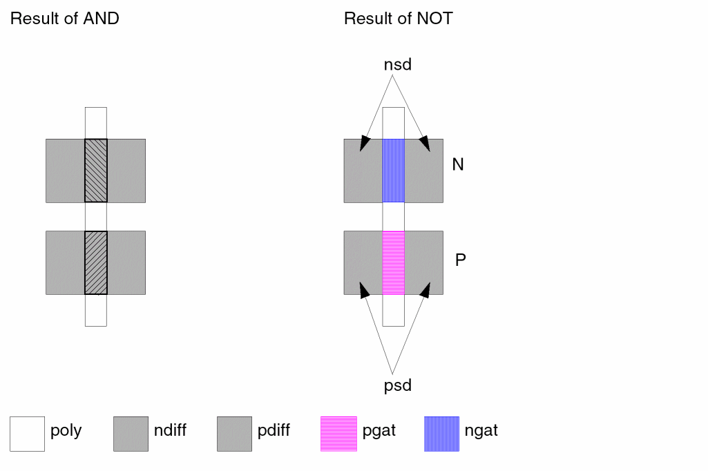
Example 2 - Optimizing the Rule Using the NOT Command
NOT      L1 T1 L2
NOT     L2 T2 L3
NOT     L3 T3 L4
NOT     L4 T4 L5
In Rule-A (the above rule) L2, L3, and L4 are not used in the other rule. You can optimize the rule as follows:
CAT    T1    T2    T3    T4    T5
NOT    L1    T5    L5
In Rule-A, Dracula requires run time for running four NOT commands, but in Rule-B, Dracula requires only one NOT command’s run time.
OCTBIAS
OCTBIASinlayer BY n1 outlayer{OUTPUTc-name l-num}
Description
Cuts all Manhattan corners on the input layer into octagonal corners with a radius of n1 and outputs the results to a new layer.
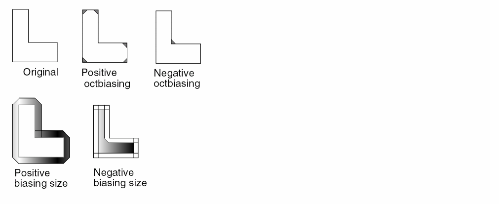
Arguments
Radius of the octagonal corners.
Sends the results of the operation to an output cell.
C-name is the name of the output cell and can have six alphanumeric characters or fewer and no special characters. L-num is the cell layer number determined by your CAD system. If your c-name is rule03 and
l-num is 5, the output cell name is rule0305.
Example
*OPERATION
.
OCTBIAS metal BY 5 omet OUTPUT OMET 50
.
SIZE[X] poly BY 10 opoly OUTPUT OPOLY 63
.
*END
OR
OR [D{n}]} layer-a layer-b trapfile {OUTPUT c-name l-num {d-num}}
Description
Creates a new layer from two other layers. The trapezoid file created by this operation consists of the total region of both layers.
Database partition functions were added for the SELECT, SIZE, and LOGICAL commands. These enhancements resolve capacity limitation issues with Dracula. This allows you to partition input layers of these functions into blocks. When you run Distributed Dracula, each block (pair) can be assigned to one processor. Specify a value between 2-10 inclusive following ‘D’ to indicate the number of partitions desired. The default value of ‘D’ is 4 if the value is omitted.
Note:- There is a performance gain in the database partition feature for SELECT in the 4.8 version. The same is not true for SIZE and LOGICAL on account of too much overhead from the pre-process (PRESEL for SIZE) and post-process (LOGMRG for LOGICAL) stages during the operations. Database partition scheme is designed specially for resolving Dracula capacity issues and is applied to flat mode only.
-
In the 4.81 and 4.9 versions, Dracula provides a method to optimize original rules and create more optimized rules to speed up run time. In the description block commands section, you can add the command
optimize-rule=YES/NO(default isNO) and speed up the run time. In the 4.81 and 4.9 Dracula versions, PDRACULA issues to you suggestions for optimizing your rule. See “Example 2 - Optimizing the Rule Using the OR Command” section for more information.
Arguments
Turns on the database partition feature
Number of blocks to be partitioned into
Layer created by the logical operation. The trapfile can have up to seven characters and no special characters. A-Z and 0-9 are permitted, but the first character must be a letter.
Sends the results of the operation to an output cell.
C-name is the name of the output cell and can have six alphanumeric characters or fewer and no special characters. L-num is the cell layer number determined by your CAD system. If your c-name is rule03 and
l-num is 5, the output cell name is rule0305.
Datatype number associated with the layer number (l-num) of the output cell. Use d-num for GDSII only. Values can range from 0 to 63.
Example 1
OR metala metalb metal
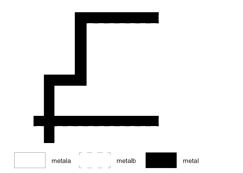
Example 2 - Optimizing the Rule Using the OR Command
You can replace several OR commands by the command, CAT+one-OR.
You can replace these original rules:
OR    FL    FLP    FL
OR    FL    ZFLP    FL
OR    FL    FLN    FL
OR    FL    ZFLN    FL
OR    FL    FLPX    FL
OR    FL    ZFLPX    FL
OR    FL    FLNX    FL
OR    FL    ZFLNX    FL
OR    FL    FLPH    FL
OR    FL    FLNH    FL
OR    FL    FPB    FL
OR    FL    FNB    FL
cat    ZFL     FLP  ZFLP  FLN  ZFLN  FLPX  ZFLNX   FLPH  FLNH  FPB  tmp1
or    tmp1      f1 f1
OVERLAP
OVERLAPinput-layer trapfile{OUTPUTc-name l-num{d-num}}
Description
Creates a layer out of overlapping polygons on the same layer. Use this command only for an input layer from your CAD graphics system.
Arguments
Layer created by this command. Can be up to seven alphanumeric characters and no special characters. The first character must be a letter.
Outputs edges to the output file in an output cell.
C-name is the name of the output cell and can have six alphanumeric characters or fewer and no special characters. L-num is the cell layer number determined by your CAD system. If your c-name is rule03 and
l-num is 5, the output cell name is rule0305.
Datatype number associated with the layer number (l-num) of the output cell. Use d-num for GDSII only. Values can range from 0 to 63.
Example
This example checks input layer diff for digitized polygons that overlap. Use to check overlaps prior to running optical PG.
OVERLAP diff difov OUTPUT ov1 50
OVL
OVL in-lay1 inlay2 {WITHIN nn} out-lay1 {out-lay2}
{OUTPUT c-name l-num {d-num} }
Description
Outputs the trapezoids from the first input layer that are overlapped or within a specific distance from those in the second input layer to one or two output layers.
Arguments
Positive value specifying the growing value of in-lay2.
Outputs non-overlapping shapes from in-lay1 (while with overlapping shapes in out-lay1).
Example
OVL CONTACT METAL WITHIN 2.0 GOODCON BADCON
Will output from CONTACT that are within 2 microns from METAL to GOODCON, and the others in BADCON.
PARAMETER CAP
PARAMETER CAP [type]value-a value-b
Description
Inputs the capacitance per unit area (value-a) and capacitance per unit perimeter (value-b). This LVS command extracts the capacitance values of the capacitors and compares these values to the schematic values. The PARAMETER CAP command works with the ELEMENT CAP command. If you do not specify PARAMETER CAP for a given ELEMENT CAP in an LVS run, the default is zero and LVS does not check capacitor value.
Arguments
The type of CAP device specified in the ELEMENT CAP command.
The capacitance per unit area of layer-a that exists between layer-b and layer-c of the ELEMENT CAP command. The value you specify for
value-a can be a floating point number (maximum 7 digits) or a floating point number followed by an integer exponent (maximum 2 digits). When you specify floating point numbers, the leading zeros are not counted in the 7-character restriction. The preprocessor rounds the value at the 7th digit. In scientific notation, the limit is 16 characters and is truncated at the 17th.
The capacitance per unit perimeter of layer-a of the ELEMENT CAP command. The value you specify for value-b can be a floating point number (maximum 7 digits) or a floating point number followed by an integer exponent (maximum 2 digits). When you specify floating point numbers, the leading zeros are not counted in the 7-character restriction. The preprocessor rounds the value at the 7th digit. In scientific notation, the limit is 16 characters and is truncated at the 17th.
Example 1
ELEMENT CAP[A] metpol metal poly
PARAMETER CAP[A] 1E-18
For LVS capacitance checking, you must use the LVSCHK or LPECHK option of CAPVAL because it specifies the value of 1E-18 per square unit.
Example 2
ELEMENT CAP[P] pl2 poly buried
PARAMETER CAP[P] 1
If you use the LVSCHK option of CAPVAL (together with *.CAPVAL in CDL netlist) and the parameter value of 1 per square unit, as shown in this example, then checking the capacitance value is equivalent to checking capacitor area. The only exception is that the VALUE= syntax, instead of the AREA= syntax, is reported in the LVS report file.
PARAMETER RES
PARAMETER RES[type]value
Description
Inputs the sheet resistance value of resistors defined by an ELEMENT RES command. This LVS command indicates the resistance values for the resistors extracted from the layout database. If you do not specify PARAMETER RES for a given ELEMENT RES in an LVS run, the default is zero, and LVS does not check the resistor value.
The unit of sheet resistance must agree with the layout unit and the resistance unit. Specify units in the Description block with the UNIT command so the calculated values agree with the schematic information.
Arguments
Type of RES device specified in the ELEMENT RES[type] command.
Sheet resistance value. If you specify this value, you must use the LVSCHK option of RESVAL. The value you specify for value-a or
value-b can be floating point (maximum seven digits) or a floating-point number followed by an integer exponent (maximum two digits). When you specify floating-point numbers, the leading zeros are not counted in the seven-character restriction. However, if the significant digits exceed the seven-digit limit, the preprocessor rounds the value at the seventh digit. In scientific notation, the limit is 16 characters and the number is truncated at the 17th.
If you specify a value of one ohm per square, you must specify the LVSCHK RESSIZE (resistor size) option.
Example 1
In the following example, LVS extracts resistance values for S type resistors using a sheet resistance value of 100 per square. When you specify sheet resistance, use the LVSCHK option of RESVAL.
ELEMENT RES[S] PRES PTERM
PARAMETER RES[S] 100
Example 2
ELEMENT RES[P] PRES1 POLY
PARAMETER RES[P] 1
If you use the LVSCHK option of RESVAL (together with *.RESVAL in the CDL netlist) and specify the parameter value of 1 ohm per square, as in this example, the resistance value check is equivalent to checking resistor size. The only exception is that Dracula reports the VALUE = syntax, instead of the NS = syntax, in the LVS report file. Remember that you are checking the resistor size.
If you want LVS to perform resistor size checking, use the LVSCHK option of RESSIZE. You do not need to specify the parameter value.
For RESVAL and RESIZE specifications, refer to the LVSCHK or the LPECHK command descriptions and Chapter 5, "Compiling Network Descriptions (LOGLVS)."
For information about resistance computation, refer to Chapter 7, “Extracting Electrical Parameters (LPE).”
PARASITIC CAP
PARASITIC CAP[R] [subType]deviceLayer termLayer1 termLayer2
Description
Defines parasitic capacitor devices resulting from overlaps or fringe effects. Add an ATTRIBUTE CAP command after the PARASITIC CAP command. ATTRIBUTE CAP associates the geometry data with the process-dependent electrical properties. ATTRIBUTE does not take units. The scale of the parasitic attribute needs to match the scale of the layout database.
Parasitic capacitors apply to stray capacitances that are either
This command does not extract capacitances if both terminals are at the same node. When extracting the overlap capacitance with fringe effect, the first terminal layer determines the possible fringe effect on the overlap capacitance. Thus, the sequence of terminal layers is important. Refer to the ATTRIBUTE CAP section for capacitance extraction of different types.
- When the poly layer is extracted for parasitic resistance, you must specify the gate layer in the CUT-TERM command.
- The first terminal layer in the PARASITIC CAP command must be derived from the cut-term connection layer by using logical operations.
For more information on extracting parasitic capacitance, see “Extracting Parasitic Capacitance” in the “Extracting RC Parasitics” chapter of the Dracula User Guide.
PARASITIC CAP with PRE
Use the PARASITIC CAP command with PRE. Resistor device layers for PARASITIC RES are allowed as terminal layers for PARASITIC CAP. These resistor device layers, in general, have no nodal information.
If the first terminal layer in a PARASITIC CAP command is a PARASITIC RES device layer, the PARASITIC CAP device layer is not required to have nodal information.
Arguments
Use this option only when extracting TPR and CLL parameters in a PRE job.
Two-character code that denotes the type of parasitic CAP device. The first character must be A-Z. The second character is optional and can be A-Z or 0-9 (excluding the number 8). This code differentiates between parasitic capacitor devices.
Device layer, one region per device. This layer defines the area and perimeter of the capacitor. The region of this layer touches or overlaps the capacitor conductor layers. Also, this device layer must carry the same nodal information as the termLayer1 terminal conductor.
Terminal conductor layer. This layer is the conductor layer for one side of the capacitor and must carry node information.
Terminal conductor layer. This layer is the conductor layer for the other side of the capacitor and must carry node information.
Example 1
In the following example, the PARASITIC capacitor of type X forms between mt1 and poly conductor layers. The device layer is mtpoly (mtpoly = metal and poly).
STAMP mtpoly BY mt1
PARASITIC CAP[X] mtpoly mt1 poly
ATTRIBUTE CAP[X] 0.0005
The two connecting layers of capacitor terminals are mt1 and poly. The device layer, mtpoly, must always carry the same electrical node of the first connecting layer, layer-b. That is, mtpoly and mt1 must convey the same node in the example. Capacitance of type X is calculated using the following formula:
(area) × (0.0005)
Example 2
In this example, the PARASITIC capacitor of [F] type is for the fringe capacitance between metal lines. The device layer is metal and the conductor layers are metal. The parasitic capacitance between metal lines is calculated for spacing distances up to 6 units.
PARASITIC CAP[F] metal metal metal
ATTRIBUTE CAP[F] 6.0 0.0005
The capacitance calculation is calculated using the following formula:
(projected metal length) x (0.005) x (1/distance between metal)
Example 3
PARASITIC CAP[mp] mtpol mt1 poly
ATTRIBUTE CAP[mp] 1E-18 1E-12
PARASITIC CAP[mp] mtpol mt1 poly
ATTRIBUTE CAP[mp] .0005 .00012
PARASITIC CAP[mp] mtpol mt1 poly
ATTRIBUTE CAP[mp] .0001234567E-9 .00007654321E-10
Remember, the leading zeros do not count in the seven significant digit restriction.
Refer to the ATTRIBUTE CAP section for more examples.
PARASITIC DIO
PARASITIC DIO [type]layer-a layer-b layer-c{layer-d} {layer-e}
Description
Defines the parasitic P-N and N-P junction diodes. You can extract the following six types of parameters from a parasitic junction diode:
Area or perimeter of a diffusion geometry not overlapped by another layer.
Area or perimeter of a diffusion geometry overlapped by a second layer, such as a metal-contact opening layer.
Area or perimeter of a diffusion geometry overlapped by a third layer, such as a buried-contact (a contact without metal) opening layer, an implant layer, or the gate region of a transistor.
Arguments
Two-character code that denotes the type of parasitic DIO device. The first character must be A-Z. The second character is optional and can be A-Z or 0-9 (except for the number 8). This code differentiates parasitic diode devices.
A1, P1 device layer, one region per device. This layer defines the parasitic diode region that touches or overlaps the anode and cathode conductor layers. Using this device layer extracts the diode area and perimeter as A1 and P1, respectively, or
This device layer must be the same layer name as the anode or cathode conductor layer, depending whether they are P-N or N-P junction diodes, and must carry nodal information.
Anode conductor layer. This layer is the conductor layer for the anode terminal and must carry node information. For a P-N diode, this layer name must be the same as the name you specified in layer-a.
Cathode conductor layer. This layer is the conductor layer for the cathode terminal and must carry node information. For an N-P diode, this layer name must be the same as the name you specified in layer-a. The preprocessor checks this syntax.
A2, P2 definition layer. This layer modifies the device layer either by overlapping or touching geometries. The extracted diode area and perimeter are modified to the following:
A1 <-- A1-A2 P1 <-- P1-P2 A2 <-- A2 P2 <-- P2
A3, P3 definition layer. This layer further modifies the device layer, after A2, P2 are invoked, either by overlapping or touching geometries. The extracted diode area and perimeter are modified to the following:
A1 <-- A1-A2-A3 P1 <-- P1-P2-P3 A2 <-- A2-A3 P2 <-- P2-P3 A3 <-- A3 P3 <-- P3
Perimeter Examples
Examples
In the following example, the PARASITIC diode of type N forms between nsrcdrn and p-substrate of a N-channel MOS process. The device layer is nsrcdrn, the anode conductor layer is psub, and the cathode conductor layer is nsrcdrn. The extracted diode area and perimeter are calculated from device layer nsrcdrn. The nsrcdrn and the cathode conduction layer have the same layer name and must carry nodal information.
PARASITIC DIO[N] nsrcdrn psub nsrcdrn
In the following example, the PARASITIC diode of type P forms between psd and nwell. The extracted diode area is calculated from device layer pdio and the perimeter and from device layer pdio minus the side where the pgate touches pdio. This effectively removes the gate perimeter region of the diode. The anode conductor is pdio, and the cathode is nwell. The device layer pdio and the anode conductor layer have the same layer name and must carry nodal information.
PARASITIC DIO[P] pdio pdio nwell pgate
PARASITIC RES
PARASITIC RES[type]layer-a layer-b{layer-c}
Description
Defines parasitic resistor devices in the layout database for PRE. An ATTRIBUTE RES command must follow the PARASITIC RES command to provide the associated process-dependent sheet resistivity used to compute the resistance values of the devices.
Dracula issues a warning if the PARASITIC CAP command is issued before any PARASITIC RES command.
For more information on extracting parasitic resistance, see “Extracting Parasitic Resistance” in the “Extracting RC Parasitics” chapter of the Dracula User Guide.
Checking Methods
Arguments
A one- or two-character code that denotes the type of parasitic resistor device. The first character must be A to Z; the second character, which is optional, can be A to Z or 0 to 9, excluding 8. Dracula uses this code to match this command with the associated ATTRIBUTE RES command.
Device layer, one region per device. This layer defines the resistor region whose parameters are to be extracted. This region must touch or cut the conductor layer.
Optional second terminal conductor layer.
Example
In this example, LPE extractions of parasitic resistance values made from PRES are computed using the sheet resistance value .01 Kohms/square.
*DESCRIPTION
UNIT = CAPACITANCE,PF AREA,U PERIMETER,M RESISTANCE,K
*OPERATION
PARASITIC RES[P] PRES PTRM
ATTRIBUTE RES[P] .01
PATHCHK
PATHCHK  {[options]}  LEVEL  n1  {trapfile} OUTPUT  c-name
l-num  {d-num}
Description
Checks MOS circuits where a node is supposed to have a path to both power and ground through one or more sources/drains of the MOS device, resistor device, BJT device, DIO device, and LDD device. This command assigns an error code to nodes without a proper path to either power or ground. The error codes are as follows:
|
Internal nodes without a path to power, ground or pads, where pads are labeled nodes reported in the 6PADL.DAT file. |
|
Arguments
Error level number (1-4). Nodes assigned this error level code are reported and placed in the output cell.
Name you designate as the output file to contain composite trapezoids. Before you do any operation on a trapfile, you need to “OR” it with itself or the substrate layer.
Sends the results of the operation to an output cell.
C-name is the name of the output cell and can have six alphanumeric characters or fewer and no special characters. L-num is the cell layer number determined by your CAD system.
If your c-name is rule03 and l-num is 5, the output cell name is rule0305.
Datatype number associated with the layer number (l-num) of the output cell. Use d-num for GDSII only; values can range from 0 to 63.
When you use ELEMENT PAD, input and output nodes with an attached ELEMENT PAD are not checked by the PATHCHK command. Also, the PATHCHK command recognizes a power node texted with :S as a power node. Therefore, error level 4 considers all pads (labeled nodes) to be potential supply nodes. The PATHCHK command level 4 does not trace paths beyond the pads. Path tracing in levels 1, 2, and 3 can be stopped only by power and ground nodes.
Example
PATHCHK     LEVEL 1    OUTPUT    pathlr 50
PATHCHK     LEVEL 2    OUTPUT    path2r 50
PATHCHK     LEVEL 3    OUTPUT    path3r 50
PATHCHK[FX] LEVEL 4    OUTPUT    path4r 50
PERI
PERI layer-a RANGE n1 n2 trapfile {OUTPUT c-name l-num (d-num}}
Description
Performs a polygon perimeter check. This operation checks polygons to determine if their perimeter is within an area range and outputs to the specified output layer.
Arguments
Flags polygon with perimeter such that n1<=PERI=>n2
Sends the results of the operation to an output cell
is the name of the output cell which has six alphanumeric characters or fewer and no special characters, l-num is the cell layer number determined by your CAD system. If your c-name is rule03 and l-num is 5, the output cell name is rule0305.
The datatype number associated with layer number (l-num) of the output cell. Use d-num for GDSII only. Values can range from 0 to 63.
Example
PERI cont RANGE 3.98 4.02 cont1
Find the 1 micron length square of the cont layer. The perimeter of a square falls within the range of 3.98 to 4.02.
PLENGTH
PLENGTHlayer-a{RANGE/NE/EQ}n1 n2{trapfile} {OUTPUTc-name l-num{d-num}}
Description
Checks the length of a series of connected edges generated from other dimensional checks with T and R options, instead of just checking the length of an edge. PLENGTH has the same format as an AREA command.
Arguments
Input layer name. This layer must be generated by an ENCLOSURE, EXTERNAL, or INTERSECT command with T and R options.
Flags the paths with length such that n1 < PLENGTH < n2.
Reports an error if any value of the layer specified is not equal to the value you specify.
Reports an error if any value of the layer specified is equal to the value you specify.
Sends the results of the operation to an output cell.
C-name is the name of the output cell and can have six alphanumeric characters or fewer and no special characters. L-num is the cell layer number determined by your CAD system.
If your c-name is rule03 and l-num is 5, the output cell name is rule0305.
Datatype number associated with the layer number (l-num) of the output cell. Use d-num for GDSII only; values can range from 0 to 63.
Example 1
This example checks for gate length less than 10.0 microns. Option TR generates the gatelen layer.
SELECT  gate    TOUCH[1:1] epi epgate
ENC[TR] epgate  diff LT .001 gatelen
PLENGTH gatelen RANGE 0.0 10.05 output d123 23
Example 2
This example checks all gate widths for less than 4 microns, including bent gates. Option TR generates the gatewd layer.
ENC[TR] gate   poly LT .001 gatewd
PLENGTH gatewd RANGE 0 4 OUTPUT gatewd 24
POSTENC
POSTENC inlayer outlayer
Description
Promotes the data to the corresponding Hcell plane if there is any cell-to-cell overlapping. You can use this command in hierarchical mode only. When you run a hierarchical DRC check, the error is reported only on the appropriate cell.
Arguments
Trapfile from the WIDTH, EXTERNAL, ENCLOSURE, and INTERSECT commands.
Examples
POSTENC poly1 polyXX

POSTENC metal1 metalXX
PROBE
PROBElabel{trapfile}{OUTPUTc-name l-num{d-num}} {&}
Description
Probes a node if the node is labeled. You must provide input text in the layout database to label a specified node. Although you can specify labels of up to 12 characters, PROBE recognizes only the first eight, so you need to make sure the first eight characters are unique. You can place the node in an output cell for visual inspection or reference.
Arguments
Text label of the node considered for the check. The text must exist in the layout database and conform to the text rules.
Name you designate as the output file to contain composite trapezoids. Before you do any operation on a trapfile, you need to “OR” it with itself or the substrate layer.
Sends the results of the operation to an output cell.
C-name is the name of the output cell and can have six alphanumeric characters or fewer and no special characters. L-num is the cell layer number determined by your CAD system. If your c-name is rule03 and l-num is 5, the output cell name is rule0305.
Datatype number associated with the layer number (l-num) of the output cell. Use d-num for GDSII only. Values can range from 0 to 63.
indicates a conjunctive rule. This command can be conjoined with other PROBE and ELCOUNT commands.
Examples
PROBE vcc OUTPUT vcc 50

PROBE clock OUTPUT clock 50
RCONNECT
RCONNECTlayer-a layer-bBYcont-layer
Description
Defines the interlayer connectivity after PRE cuts parasitic resistors from the original conduction layers. It reconnects the layers after subnodes have been cut from the original conduction layers.
The syntax of the command is similar to that of the CONNECT command. Layers in the RCONNECT commands must include nodal information extracted from the original conduction layers involved in parasitic extraction.
All PRE runs must include the RCONNECT command because RCONNECT identifies the run as a PRE run to PDRACULA.
Checking Methods
Arguments
Name of the first input layer. The layer must have nodal information.
Name of the second input layer. The layer must have nodal information.
Specifies a layer that has been previously defined and consists of the contacts that connect layer-a and layer-b.
Multiple RCONNECT commands with the same cont-layer can have only one master layer and can connect from the master layer to any other layers. For more details, refer to the CONNECT command description in this chapter and the CONNECT-LAYER command description in the “Input-Layer Block Commands” chapter.
Example
The POLY interconnect has been split into parasitic resistors and resistor terminals. The terminal layer created after the split is PTRM. The original connectivity was defined by the following:
CONNECT METAL POLY BY MCO
CONNECT METAL DIFF BY MCO
CONNECT POLY DIFF BY EPI
To reconnect the layers after the split layers and subnodes have been created, PTRM replaces POLY in the RCONNECT commands:
STAMP PTRM BY POLY
RCONNECT METAL PTRM BY MCO
RCONNECT METAL DIFF BY MCO
RCONNECT PTRM DIFF BY EPI
The STAMP command gets back nodal information on the layer PTRM from POLY if PTRM lost it in the extraction process.
RECTCHK
RECTCHK[OPTION] layer {WIDLEN NE/EQ val1 val2} {WIDTH NE/EQ/LT/RA/GT val1 {val2}} {LENGTH NE/EQ/LT/RA/GT val1 {val2}} {trapfile} {OUTPUT err lay}
Description
Checks rectangle shape, especially for contact/via layers, in flat mode only. Without any additional options the behavior is as follows:
-
If there are no
WIDTH/LENGTH/WIDLENlimitations it reports all non-rectangle shapes. -
If there is at least one of
WIDTH/LENGTH/WIDLENlimitations, it reports all non-rectangle shapes and all rectangle shapes which satisfy limitation.
Arguments
Example 1
RECTCHK contact WIDLEN NE 3 3 OUTPUT err 1
; Check the size of contact 3x3; Butted contacts are errors.
Example 2
RECTCHK[R] layer WIDTH NE 3 LENGTH GT 6
(It’s an OR operation, not an AND operation.)
The width must be 3, and length cannot be longer than 6. Don't report it if it is not a rectangle. You no longer need to use WIDTH and AREA to do this kind of check.
Example 3
RECTCHK[A] layer WIDTH LT 3 LENGTH GT 6 (it's AND)
Select rectangles with WIDTH smaller than 3 and LENGTH greater than 6.
Example 4
RECTCHK[T] ring WIDTH NE 1.2 OUTPUT err 1
Example 5
RECT [D ] poly1 WIDTH LT ..18 OUTPUT NPE4 46
In this example, distance A,D will be checked as a length while distances B,C and E,F will be checked as widths. Any other shape is not considered a donut by [D ] option.
RELOCATE
RELOCATElayer-aBYX Y trapfile{MAG =scale}
Description
A Dracula operation that creates a new layer from another layer. The trapezoid file consists of data from layer-a shifted to a new x,y position or data from layer-a with each of its vertices multiplied by the specified scale.
Arguments
New location of layer-a data that is shifted by natural units specified for X and Y.
Trapezoid file name. Consists of trapezoidal data shifted and/or magnified. Trapfile can have up to seven characters and no special characters. A-Z and 0-9 are permitted, but the first character must be a letter.
Optional magnification factor. Default magnification is equal to unity. Accept only a scale of up to three decimal values.
new x = (old x).(scale)+ X
new y = (old y).(scale)+Y
Examples
This example shifts the data in the metal layer by a negative 5 units in the x direction. Outputs the data to the met5 layer. Does not magnify.
RELOCATE metal BY -5 0 met5
This example magnifies the active layer by 5 times. Outputs the data to the active5 layer.
RELOCATE active BY 0 0 active5 MAG = 5
This example magnifies the cont layer by 2 times. Shifts the data by negative 1 unit in the x direction and negative 2 units in the y direction. Outputs the final data to the newcont layer.
RELOCATE cont BY -1 -2 newcont MAG=2
RLENGTH
RLENGTHlayer-a{&layer-a1} GT/GE/ LT/LE/ RANGEn1{n2} {OUTPUTc-name l-num{d-num}} {&}
Description
This command is similar to LENGTH, but it is used with EXT while LENGTH is only applied to a single layer. This command checks the length dimension based on the same region. If the error flags are created on the same region, they are merged to form the length of the error flag.
Arguments
Renames (conjunctive rename) the layer containing the error flags. The original layer name is then restored to the original layer. No spaces are allowed between the layer-a and &layer-a1 names, for example, poly&rpoly.
Measures between all nonconsecutive pairs of inside edges of the polygons of the input layer. Compares the measurements against the limits you specify and flags violations.
GT means that error segment length greater than n1 layout units causes a violation. GE means that length greater than or equal to n1 layout units causes a violation.
LT means that length less than n1 layout units causes a violation. LE means that length less than or equal to n1 layout units causes a violation.
RANGE means that length greater than n1 and less than n2 layout units causes a violation (n1 < range <n2).
Sends the results of the operation to an output cell.
C-name is the name of the output cell and can have six alphanumeric characters or fewer and no special characters. L-num is the cell layer number determined by your CAD system.
If your c-name is rule03 and l-num is 5, the output cell name is rule0305.
Format of the output is the same as the original database.
Datatype number associated with the layer number (l-num) of the output cell. Use d-num for GDSII only. Values can range from 0 to 63.
Example
EXT METAL1 LT 0.8 &
RLENGTH METAL1 GT 2.0 OUTPUT err 01
RSPFSELECT
RSPFSELECT {[opt]} {INST=YES/NO} filename
Description
Generates a reduced standard parasitic file (RSPF) for HPRE. Use this command in composite mode only.
The default unit of input capacitance is Farad, and the default unit of resistance capacitance is ohm. The default unit for reduction algorithms is PF, and the default for resistance is ohm. Dracula converts input resistance capacitance values to the corrected scale during the reduction process. Dracula converts output resistance capacitance values from reduction algorithms back to the specified scale before RSPF is written out. Therefore, you must carefully specify the scale in the UNIT command in order to get meaningful resistance capacitance values.
Arguments
Specifies whether to backannotate (S option) or not (no option).
The default is YES and the instance section will be output. The user can delete the instance section by using the NO option.
Sends the results of the operation to this file. Dracula appends a .dat to the file specified.
Example
This example creates a reduced parasitic file named RSPF.dat with backannotation.
RSPFSELECT[S] RSPF
SAMELAB
SAMELAB {trapfile} OUTPUT c-name l-num {d-num}
Description
Detects when the same label is assigned to multiple nodes. This situation usually occurs when
SAMELAB outputs multiple nodes with the same label in an output cell.
Text involved with SAMELAB is discarded after this check and thus the text no longer exists for any other ERC checks. SAMELAB problems must be cleared of errors before proceeding to inspect other ERC checks. MULTILAB and SAMELAB errors lead to false LVS or LPE output, so you must clear their errors before going on to LVS or LPE. For more information about ERC checks, refer to Chapter 4, “Checking Electrical Rules (ERC).”
You should include both MULTILAB and SAMELAB commands in an LVS or LPE rules file.
Arguments
Name you designate as the output file to contain composite trapezoids. Before you do any operation on a trapfile, you need to OR it.
Sends the results of the operation to an output cell.
C-name is the name of the output cell and can have six alphanumeric characters or fewer and no special characters. L-num is the cell layer number determined by your CAD system. If your c-name is rule03 and l-num is 5, the output cell name is rule0305.
Datatype number associated with the layer number (l-num) of the output cell. Use d-num for GDSII only. Values can range from 0 to 63.
Example
In this example, different nodes with the same label are output to the opens40 error cell on the layer beginning with layer 40 and ending at a higher layer number depending on the number of CONNECT-LAYERS and contact layers.
SAMELAB OUTPUT opens 40
SCONNECT
SCONNECTupper-layer lower-layerBYcontact-layer{LINK label}
Description
Creates a connection between a conductor layer and a soft connect layer. SCONNECT allows unidirectional passing of nodal information according to the CONNECT-LAYER sequence, that is, passing nodal information from the conductor to the soft connect layer, but not the reverse.
If multiple SCONNECT trapezoids are reported in the .ERC file, Dracula reports the following warning in the .lvs file:
*/W* WARNING :: SOFT-CONNECTING MULTIPLE NODES IN UPPER LAYERS TO ONE POLYGON REGION IN: PWELL
To use the global majority rule for SCONNECT conflict resolution, see GLOBAL-SCONNECT.
Arguments
Lower layer name. Connectivity passes from upper-layer to lower-layer (soft connect layer) but not the reverse.
Previously defined layer that consists of the contacts that connect upper-layer to lower-layer. Must have at least three characters.
As an example, you can make a soft connection when you use one NWELL region to connect (and pass nodal information) between two separate NSRCDRN regions. In the regular nodal passing scheme, Dracula treats the three regions as one electrical node. However, the SCONNECT command assigns different node numbers to the regions.
When the nodes have different numbers, instead of merging all connecting nodes, SCONNECT picks and pushes one node number in NSRCDRN onto NWELL. Dracula selects the node number that contains the most trapezoids of connected nodes among the soft-connected layers.
You can then use the SOFTCHK command to report the violation geometries in one or both connect layers. You can also use the ABORT-SOFTCHK command to stop the job when soft connection violations exist. If you ignore these violations, the errors might resurface during LVSCHK. Therefore, it is good practice to stop the job and fix any soft connection violations.
When you use the U option in SOFTCHK, this command outputs trapezoids whose node number contains the fewest number of trapezoids among those node numbers that are soft connected by the same region in the lower layer.
Links floating substrates (lower- layer) to label (power or ground) unless the substrates are assigned text other than power or ground.
Example 1
In this example, nodal information passes from nsd to nwell and not in reverse.
*OPERATION
.
.
AND NWELL NSD NPNWELL
AND PSUB PSD PINSUB
;
CONNECT METAL PSD BY CONTS
CONNECT METAL NSD BY CONTS
CONNECT METAL POLY BY CONTS
CONNECT SCMET METAL BY VIA
SCONNECT NSD NWELL BY NPNWELL
SCONNECT PSD PSUB BY PINSUB
;
SOFTCHK NWELL OUTPUT[U] ERR1 50
SOFTCHK PSUB OUTPUT[U] ERR2 50
;
Example 2
This example links NWELL to VDD unless the nwell is assigned another text.
*DESCRIPTION
...
GEN-TEXT-FILE = GENTXT.OUT
GEN-TEXT-WIRE = YES
...
*END
*INPUT-LAYER
...
GEN-TEXT-LAYER = NWELL...METAL...
CONNECT-LAYER = NWELL ...METAL...
...
*END
*OPERATION
...
SCONNECT METAL NWELL BY NWCONT LINK VDD
...
*END
Example 3
This example demonstrates incremental connection. The connection is rebuilt because the AVSS label needs to be excluded from the IPDEF layer.
*DESCRIPTION
...
ALLOW-RECONNECT = YES
...
*END
*OPERATION
...
CONNECT        ALMI    IPF     BY      PFCON
CONNECT ALMI ADEF BY CWW
CONNECT ADEF IPDEF BY PDCT
CONNECT ADEF INDEF BY NDCT
SELECT IPDEF LABEL AVSS? xIPDEF
NOT IPDEF xIPDEF VSIPDEF
; connection rebuild starting point
CONNECT ALMI IPF BY PFCON
CONNECT ALMI ADEF BY CWW
CONNECT ADEF IPDEF BY PDCT
CONNECT ADEF INDEF BY NDCT
; connection rebuild end point
SCONNECT INDEF INWELL BY SSX
SCONNECT VSIPDEF PWELL BY PPX
SCONNECT VSIPDEF KIBAN BY KKX
SOFTCHK INWELL OUTPUT[U] NST 101 1
SOFTCHK PWELL OUTPUT[U] PST 102 1
SOFTCHK KIBAN OUTPUT[U] KST 103 1
...
*END
SELECT
For the syntax for SELECT, see Option I through Option IX in the sections below.
Description
Selects a group of polygons from a layer and creates a trapezoid file with the new layer. SELECT is an area-relation command. For example, if a polygon on layer-a is related to layer-b, the layer-a polygon is output. You can use this command to perform selective operations that cannot be done by logical operations, such as sizings, spacing checks, and conjunctive rules.
Nodal information associated with the selected polygons is passed to the trapezoid file. Database partition functions were added for the SELECT, SIZE, and LOGICAL commands. These enhancements resolve capacity limitation issues with Dracula. This allows you to partition input layers of these functions into blocks. When you run Distributed Dracula, each block (pair) can be assigned to one processor. Specify a value between 2-10 inclusive following ‘D’ to indicate the number of partitions desired. The default value of ‘D’ is 4 if the value is omitted.
Note:- There is a performance gain in the database partition feature for SELECT in the 4.8 version. The same is not true for SIZE and LOGICAL on account of too much overhead from the pre-process (PRESEL for SIZE) and post-process (LOGMRG for LOGICAL) stages during the operations. Database partition scheme is designed especially for resolving Dracula capacity issues and is applied to flat mode only. The performance of the SELECT command in the 4.8 version is equal to the 4.6.0698, 4.6.0998, and 4.6.1298 versions and is 5 to 20 times faster than the 4.7 release.
-
In the 4.81 and 4.9 versions, Dracula provides a method to optimize original rules and create more optimized rules to speed up run time. In the description block commands section, you can add the command
optimize-rule=YES/NO(default isNO) and speed up the run time. In the 4.81 and 4.9 Dracula versions, PDRACULA issues to you suggestions for optimizing your rule. See the section, “Example 2 - Optimizing the Rule Using the SELECT Command” for more information.
Option I - Syntax for SELECT
SELECT[N] layer-a relation layer-b trapfile {OUTPUT c-name
l-num {d-num}}
Turns on node-based rather than polygon-based selection. Selection is based on nodal numbers rather than region numbers. Specify this option after the CONNECT command in the operation block of a rule file. PDRACULA issues a warning message if the order in which you specified these commands is incorrect.
Returns all shapes on layer-a that
Specifies layer-a polygon that is totally inside a layer-b polygon. Outputs the layer-a polygon and inside-touch layer-b.
Specifies layer-a polygon that is totally outside a layer-b polygon. Outputs the layer-a polygon and touch layer-b.
Specifies layer-a polygon that has its entire outside surface exactly touching the outside surface of layer-b (for example, a layer-a polygon that exactly fits in the hole of a donut-shaped layer-b polygon). The selected layer-a polygons are outside and touch.
Layer created by the SELECT operation. The trapfile can have up to seven characters and no special characters. You can use A-Z and 0-9, but the first character must be a letter.
Sends the results of the operation to an output cell.
C-name is the name of the output cell and can have six alphanumeric characters or fewer and no special characters. L-num is the cell layer number determined by your CAD system. If your c-name is rule03 and
l-num is 5, the output cell name is rule0305.
Datatype number associated with the layer number (l-num) of the output cell. Use d-num for GDSII only. Values can range from 0 to 63.
Option II
SELECT {[D{n}]|[N]} layer-a relation {[n1:n2]} layer-b trapfile {OUTPUT c-name l-num {d-num}}
SELECT’s D option (SELECT[D]) is now used for the database partition for SELECT. It can apply to all SELECT options except the following:
This option selects a range of instances that satisfy the selective condition. This option applies to the CUT, TOUCH, and ENCLOSE relationships.
Turns on the database partition feature
Number of blocks to be partitioned into
Turns on node-based rather than polygon-based selection. Selection is based on nodal numbers rather than region numbers. Specify this option after the CONNECT command in the operation block of a rule file. PDRACULA issues a warning message if the order in which you specified these commands is incorrect.
Returns all shapes on layer-a that
Example (see the Figure that follows).
 INPUT-LAYER
 ...
 CONT = 5
 MET1 = 6
 VIA  = 7
 MET2 = 8
 ...
 CONNECT-LAYER = POLY MET1 MET2
*END
*OPERATION
 ...
 CONNECT MET2 MET1 BY VIA
 CONNECT MET1 POLY BY CONT
 ...
 SELECT[N] MET1 OVERLAP POLY M1NOVC OUTPUT M1NOVC 63
 SELECT MET1 CONN POLY M1CONC OUTPUT M1CONC 63
 ...
*END
The example illustrates the functionality and differences of SELECT[N] and SELECT .. CONN.
The SELECT[N] command will first include MET1 #1 and MET1 #3 into M1NOVC because they both overlap poly (the fact that MET1 #1 connects to poly with contact is merely coincidental). By virtue of the ’CONNECT MET2 MET1 BY VIA’ command, MET1 #1 and MET1 #2 are part of the same net; the same is true for MET1 #3 and MET1 #4. Since MET1 #2 is part of the same node as MET1 #1, MET1 #2 will also be included in M1NOVC. MET1 #4 will also be included in M1NOVC because it is part of the same node as MET1 #3.
The SELECT ... CONN command will first include MET1 #1 into M1CONC because of the “CONNECT MET1 POLY BY CONT” command. MET1 #3 is not connected to POLY and is therefore not considered. By virtue of the “CONNECT MET2 MET1 BY VIA” command, MET1 #1 and MET1 #2 are part of the same node; MET1 #2 will also be included in M1CONC.
The range of instances. Outputs layer-a polygons that fall within the condition range of layer-b. The range values (n1 and n2) are inclusive and must be integers. Zero is not allowed.
Specifies layer-a polygon that has portions both inside and outside layer-b.
Specifies layer-a polygon that touches only from the outside of a layer-b polygon. Does not include a layer-a polygon that both touches and cuts a polygon of layer-b.
Specifies layer-a polygon that encloses a polygon of layer-b. Includes a layer-a polygon that is inside and touching layer-b.
Specifies layer-a polygon that overlaps (including TOUCH, CUT, ENCLOSE, and INSIDE) a polygon of layer-b. The overlap relation includes all relationships except for those of layer-a polygons entirely outside of layer-b polygons.
Currently, the SPACING module does not have a database partition feature. However, since EXT[E] is translated into SELECT by PDRACULA, it is possible to have a data partition for EXT[E]. EXT’s D option must combine with the E option (EXT[DE]).
| Total | PRESEL | POSCAT | SELECT | |
|---|---|---|---|---|
| SELECT | ||||
| SELECT[D] | ||||
| SELECT[D2] | ||||
| SELECT[D3] |
EXT[TOE] = EXT with [T], [O], and [E] options turned to on
where T represents touch, 0 represents overlap, and E represents fully enclosed. SELECT is slow. The flow in the 4.7.0399 version uses one AND and one SPACING. AND is faster than SELECT.
Option III
SELECT layer-a LABEL{[R]} label-name trapfile {OUTPUT c-name l-num {d-num}}
This option selects all layer-a polygons that are part of the label-name texted net. You must establish nodal connectivity on layer-a with the CONNECT, SCONNECT or STAMP command before using this option.
Selects all layer-a polygons that physically attach to the label-name text that establishes the net. You must specify the ATTACH command for layer-a in the INPUT-LAYER block.
The text label of the net to check.
Example
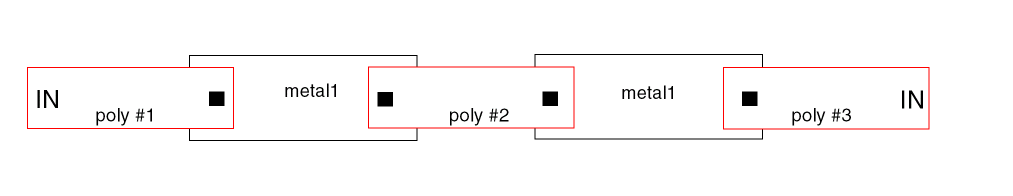
*INPUT-LAYER
...
poly = 5
contact = 6
metal1 = 7
text = 10 attach = poly
...
CONNECT-LAYER = poly metal1
*END
*OPERATION
...
CONNECT poly metal1 BY contact
...
SELECT poly LABEL IN layerA
SELECT poly LABEL[R] IN layerB
...
*END
The LABEL operator will include all three poly shapes (poly #1, poly #2 and poly #3) into layerA because they are all part of the texted net IN.
The LABEL[R] operator will only include the poly #1 and poly #3 shapes into layerB because the IN text attaches only to these two shapes.
Option IV
SELECT layer-a VERTEX [n1:n2] trapfile {OUTPUT c-name
{d-num}}
This option selects all layer-a polygons that satisfy the vertex count. SELECT counts the vertices after merging the polygon vertices. SELECT counts double digitized vertices only one time.
A layer-a polygon that satisfies the vertex count range. A rectangular polygon has four vertices.
The range of vertex counts. Outputs layer-a polygons that fall within the count range. The range values (n1 and n2) are inclusive and must be integers. Zero is not allowed.
Option V
SELECT layer-a ANGLE [n1] output-layer {OUTPUT c-name l-num
{d-num}}
This option lets you separate all-angle geometries from Manhattan geometries.
Specifies which angled geometries to separate. You can specify one of the following options:
Option VI
SELECT layer1 BY layer2 LABEL([t] | [t’]) (label|label-list) outLayer {OUTPUT c-name l-num {d-num}}
Use this command when you specify the IDTEXT command in the Input Layer block.
Layer name from which objects are selected.
Selects objects texted by the given labels.
Selects objects that are not texted by the given labels.
Any label, which can include meta characters such as ?.
A list of up to a maximum of 20 labels ({label...}).
Option VII
SELECT {NOT} layer-a relation layer-b trapfile {OUTPUT c-name
l-name {d-name}}
This option lets you output the complemented outputs without using another NOT command.
Use this command to provide complemented output with the single rule.
Option VIII
SELECT layer-a CONN layer-b output-layer {OUTPUT c-name l-name {d-num}}
This option lets you select geometric based on layer connectivity.
Output layer-a polygons that are connected to layer-b. The output is a subset of layer-a.
Option IX
SELECT layer-a NODE schematic-name output-layer
This option selects layer-a layer geometries that are cross referenced to specified schematic names. LVSCHK is necessary before you apply this command.
Name of the specified schematic
Examples
Example 1
This example selects all nplus polygons with an annotated text string beginning with the characters hv. Outputs these polygons on hvnplus.
SELECT   nplus   INSIDE   pwell   nsrcdrn
SELECT   nplus   OUTSIDE  pwell   nguard
SELECT   nplus   LABEL    hv?     hvnplus
This example selects metal polygons with annotated pads. Outputs these polygons on pads.
SELECT metal LABEL ?:? pads
This example selects transistors that have one source/drain.
SELECT gate TOUCH[1:1] nsrcdrn cap
This example selects a poly polygon with res text attached as resistor layer, polres.
SELECT poly LABEL[R] res? polres
In the following example, the gdcont layer contains quadrilateral contacts.
SELECT contact VERTEX[4:4] gdcont
In the following example, the bad1 and drc317 layers contain contacts with three or fewer vertices.
SELECT contact VERTEX[1:3] bad1 OUTPUT drc317
In the following example, the bad2 and drc418 layers contain contacts with more than four vertices.
SELECT contact VERTEX[5:999] bad2 OUTPUT drc4 18
In the following example POLY is selected and cross-referenced to the schematic name VDD* to output layer POLY1.
*OPERATION
...
LVSCHK
...
SELECT POLY NODE VDD* POLY1......
*END
Example 2 - Optimizing the Rule Using the SELECT Command
You can optimize the following two rules
SELECT layer-a relation layer-b layer-c
NOT layer-a layer-c layer-d
(and layer-c is not used for the other rule)
to one rule using the following command
SELECT NOT layer-a relation layer-b layer-d
The above optimization will save you the run time for one NOT command.
SELECT Command with CONN
In previous versions of the tool, if you used SELECT layA CONN layB layC and layA or layB did not have nodal information, the SELECT stage terminated.
In the 4.8 version of Dracula, you can set the environment variable DRAC_SELCONN_NOTABORT. SELECT CONN runs without terminating the process. The trapezoid without the nodal information is output to the log file.
SHRINK
SHRINKinput-layer dx dy{dx2 dy2}{trapfile} {OUTPUTc-name l-num{d-num}}
Description
Undersizes a single side of a layer. The dx and dy values determine the direction and amount the data shrinks.
Refer also to the GROW command description in this chapter.
Arguments
Amount to undersize the layer. This value is a real number in microns or mils. This is the unit set by SCALE.
Specifies the second set of direction. All values must be positive.
Name of the output cell. You can optionally output the sized data to a cell.
Layer number of the output cell.
Datatype number associated with the layer number (l-num) of the output cell.
Example
*DESCRIPTION
SCALE = 0.001 MIC
RESOLUTION = 0.001 MIC
MEBES-UNIT = 0.25 MIC
*END
*OPERATION
...
SHRINK layer3 1 1.5 layer4  ;Shrink right edge 1 micron.
...                         ;Shrink top edge 1.5 micron.
*END
SIZE
SIZE {[options]} input-layer BY n1 {TRUNCATE {trunc_value}} {trapfile} {OUTPUT c-name l-num {d-num}}
SIZE {[options]} input-layer BY n1 STEP {step_value/AUTO} {TRUNCATE {trunc_value}} {output-layer} {trapfile} {OUTPUT c-name l-num {d-num}}
SIZE {[options}] input-layer-a {WITHIN input-layer-b} BY n1 [STEP step_value] {TRUNCATE {trunc_value}} {trapfile} {OUTPUT c-name l-num {d-num}}
SIZE[D{n}] input-layer BY n {STEP step-value} {TRUNCATE {trunc_value}} {trapfile} {OUTPUT c-name l-num {d-num}}
SIZE input-layer DOWN-UP BY n1 {TRUNCATE {trunc_value}} {trapfile} {OUTPUT c-name l-num {d-num}}
Description
Creates a new layer from another layer. This command oversizes or undersizes the new layer by a specified number of layout units and moves the sides of the polygon perpendicularly. The numerical sign determines whether to oversize (+) or undersize (-) the polygon.
Database partition functions were added for the SELECT, SIZE, and LOGICAL commands. These enhancements resolve capacity limitation issues with Dracula. This allows you to partition input layers of these functions into blocks. When you run Distributed Dracula, each block (pair) can be assigned to one processor. Specify a value between 2-10 inclusive following ‘D’ to indicate the number of partitions desired. The default value of ‘D’ is 4 if the value is omitted.
Note:-
There is a performance gain in the database partition feature for SELECT in the 4.8 version. The same is not true for SIZE and LOGICAL because of too much overhead from the pre-process (PRESEL for SIZE) and post-process (LOGMRG for LOGICAL) stages during the operations. Database partition scheme is designed specially for resolving Dracula capacity issues and is applied to flat mode only. Currently, the database partition feature for SIZE does not support other options.
SIZE does not output text information.
When sizing databases with layers digitized with arbitrary angles (circles) or when sizing databases with cell placements not on fixed grids (some auto-routers), set the RESOLUTION command in the Description block at 0.005 microns or less. This setting alerts the SIZE command to handle round-off problems and to effectively “lock” the adjacent line segments.
TheWITHINoption works only in flat mode. It supports step-wise sizing to avoid significant round-off effects resulting from large sizing and to improve SIZE performance for large values.
When using theSIZE WITHINoption, a contact can change size and fill the space of any portion of the shape it is within, including ring (donut) shapes, U shapes or L shapes. The contact can "jump over" any gap (notch) that exists for any single area (contacts cannot jump over to adjacent but different areas). If you have ring, U, or L shapes, it is best to use the STEP x option with theWITHINoption. The value of the STEP size x should be less than the minimum external notch spacing of the ring or U shape so that each step of the sizing cannot jump across the gap. - When using the SIZE command on a 45-degree angle, oversizing and undersizing might produce a different shape than the original. When you oversize a 45-degree angle, it snaps to the grid, which might modify the shape. If you then undersize this layer, it will snap to the grid again, resulting in a different shape than you started with.
-
In the 4.81 and subsequent versions, Dracula provides a method to optimize original rules and create more optimized rules to speed up run time. In the description block commands section, you can add the command
optimize-rule=YES/NO(default isNO) and speed up the run time. In the 4.81 and 4.9 Dracula versions, PDRACULA issues to you suggestions for optimizing your rule. See Example 13 - Optimizing the Rule Using the SIZE Command of this section. -
When you size non-orthogonal polygons, set the value of the
RESOLUTIONcommand to the same value as that of theSCALEcommand; otherwise, Dracula may distort the resulting shape. For example, ifSCALE = 0.001MICRON, theRESOLUTIONcommand should also be set toRESOLUTION = 0.001MICRON.
If you need to know if any polygons or cell placements are off-grid, add this command:FLAG-OFFGRID = YES
where value is the grid value in the Description block.value
Here is an example:FLAG-OFFGRID = YES 0.01
Do not specifyMICRONorMILafter the grid value, since the scale factor is already implied in theSCALEcommand.
Arguments
Adjusts the width of error flags that result from spacing checks with the R’ option.
Turns onS the database partition feature.
Represents the number of blocks to be partitioned.
Sizing only for edges as projections. This option is used with the SPACING[D] option, which outputs error flags in trapezoid format that contain information for edge sizing later on. Edge size is only supported at flatten mode, and can only produce trapezoid output, not polygon output.
Adjusts the length of error flags that result from spacing checks with the R’ option.
Prevents polygon data output from the SIZE command from being included in the OUTDISK file. Use this option only if you want to fracture sized polygon data and do not want this data included in the OUTDISK file. Use this option only when you specify an output layer.
(Oversize only) Sizes the layer but does not merge the sized data. Generates only the sized geometries that overlap. You can specify only the trapfile name.
When oversizing a layer, some polygons might extend into each other. SIZE forms one “clean polygon” from the potential overlap. When undersizing a layer, polygons with complex shapes tend to separate. SIZE does not create gaps on polygon cut lines, but a gap can result if part of the polygon width undersizes to 0 or less. This command prevents polygons from turning inside-out.
(Undersize only) Sizes the layer as “pre-merged” data (as opposed to “merged” data). Therefore, the abutted polygons generate gaps where previously abutted. Apply the P option to the original layer only, not to the derived layer. When specifying the P option, input and output layers must be different; otherwise, conflicts might arise in later sizing operations.
R (Undersize only) Reverses sizing capability. When doing undersize, if the sizing dimension causes the geometry width to go down to zero, this option allows it to reverse direction. This option works for manhattan shapes only. Result layer will contain processed manhattan shapes from input layer. All non-manhattan shapes will generate new layer which name will combined from original layer name and "-NM". E.g. for "M1" layers non-manhatten shapes will form "M1-NM" layer.
Outputs trapezoid shapes to SIZE output file, not a polygon file. If you specify T, you must specify OUTPUT. If you specify T, you cannot specify any other option (A, B, G, and so on).
Specifies a minimum polygon cut-line width of 0.5 microns instead of the default of 1 micron. Use this command option when sizing very dense layers such as diffusion, poly, or metal in a MOS memory layout. For more information, refer to the SIZE-MIN-WIDTH command in Chapter 11, “Description Block Commands.”.
Specifies the input layer name.
Specifies that the sizing of input layers truncates acute angles. Sizing by positive value means cutting convex angles. Sizing by negative value means cutting concave angles.
Optional value, that determines maximum distance of acute-angles that will not be truncated. The truncation distance = n1*trunc_value. The default value is sqrt(2). (It means that all angles less than 45 degrees will be truncated)
Specifies that the sizing of input-layer-a is limited to the enclosing input-layer-b. This function efficiently checks latch-up problems.
Number of layout units to oversize or undersize the input-layer.
Specifies that the sizing of the input-layer is to be step-wise, performing a series of size operations using step_value until the overall distance n1 is reached. When you specify a SIZE WITHIN operation, a logical AND operation with input-layer-b is followed by the size operation.
If you are sizing over 10 microns and you do not use STEP, huge vertex polygons are created, which cause slow performance and undesirable sizing.
Dimension by which to size in each STEP. Specifying this argument splits the SIZE function into a number of SIZE and logical AND functions. These functions are internally performed by Dracula to increase the accuracy of sizing for U-shaped geometries.
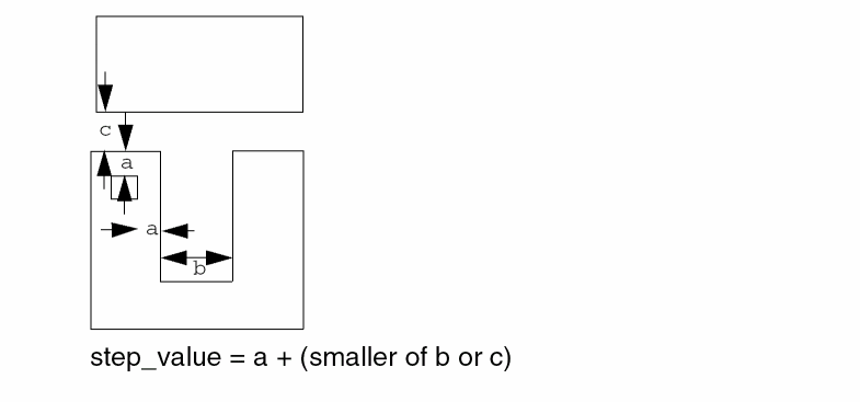
When you specify STEP AUTO, the value of STEP is automatically adjusted according to your rules file. Use AUTO for large value sizing only (sizing over 10 microns).
Trapezoid file created by the resizing operation.
Sends the results of the operation to an output cell.
C-name is the name of the output cell and can have six alphanumeric characters or fewer and no special characters. L-num is the cell layer number determined by your CAD system. If your c-name is rule03 and l-num is 5, the output cell name is rule0305.
The output cell (c-name) usually generates three cells that contain the total sized data. The data is in PG-compatible polygon format. The three cells are suffixed as follows:
This conservative SIZE algorithm checks the sized data for the following:
Datatype number associated with the layer number (l-num) of the output cell. Use d-num for GDSII only; values can range from 0 to 63.
Keyword implemented to filter the smaller redundant parts of a big polygon. First of all, Dracula cuts the polygon into pieces by both vertical and horizontal directions according to each vertices’ coordinations, and then calculates the width of each piece to see if it will remove it or not.
This option helps to extract big geometries that satisfy a specific width condition. Two similar ways to achieve this functionality is to either:
Use the WIDTH check with the [R] option to output the required segments. Refer to the WIDTH[R] command in this chapter for more information.
Do a SIZE-DOWN operation, followed by a SIZE-UP operation. This method is more accurate, but introduces performance problems with dense layers like METAL. This option is limited to FLAT mode only.
The result of a single SIZE DOWN-UP is not intended to simulate that of a SIZE DOWN followed by a SIZE UP operation. Actually, the output is more like a WIDTH check with the [R] option. For example,
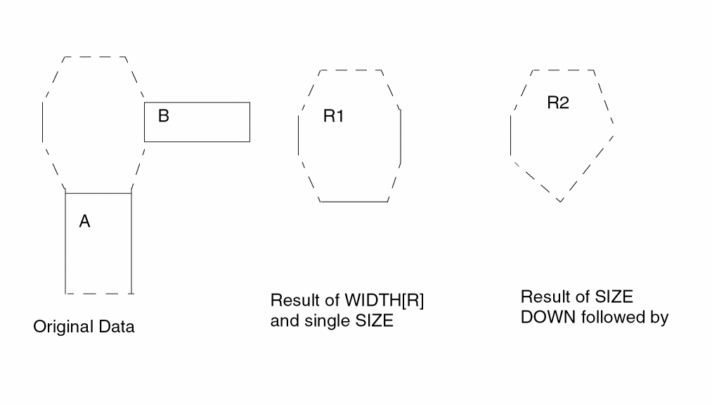
The result of R1 is more preferable than R2 because two consecutive SIZE operations will probably give rise to acute angles and cause false errors in subsequent checks.
For example, the following rules used in one case helped to eliminate false errors caused by acute angles induced by two SIZE DOWN-UP commands:
WIDTH[R] MT1 LT 10.0 MT1L10
NOT MT1 MT1L10 MT1G10
SIZE MT1G10 BY -4.95 UM1G10
SIZE UM1G10 BY 4.95 OM1G10
EXT OM1G10 MT1 LT 1.3 OUT D6D 53 ;
If MT1 is a very dense layer, it takes longer in the above example to do the WIDTH[R] operation. But, if a single SIZE DOWN-UP command is used it takes hardly 30 seconds and the speed is optimized by 160 times with the result being almost as accurate as MT1G10 without inducing any acute angle.
| Total | PRESEL | POSCAT | SIZE | |
|---|---|---|---|---|
| SIZE | ||||
| SIZE[D] | ||||
| SIZE[D2] | ||||
| SIZE[D3] |
Example 1
This example sizes all poly data, outputs it to the unpoly layer, and creates upoly30G, upoly30A (sometimes), and upoly30R (rarely).
SIZE poly BY -.1 unpoly OUTPUT upoly 30
Example 2
In this example, the T option specifies that output cell OMETALIO.DAT is a polygon file that contains trapezoid shapes instead of a normal polygon file.
SIZE[T] METAL1 BY 5 OMETAL OUTPUT OMETAL 10
Example 3
This example sizes cont layer shapes by 25 microns, but keeps the resulting cont shapes within their enclosing met1 shapes.
SIZE cont WITHIN met1 BY 25.0 conts
Example 4
The following example sizes the cont layer shapes by 25 microns in steps of 4.9 microns, keeping the resulting shape within the enclosing met1 shape at each step. This results in growing around the notch (rather than skipping over it), but this takes Dracula longer to execute than the method used in Example 3. The value of 4.9 microns is chosen to be just less than the minimum met1 notch allowed in the process. Therefore, within any one step, the sized shape cannot skip across the notch.
SIZE cont WITHIN met1 BY 25.0 STEP 4.9 conts
Example 5
SIZE poly BY -1 unpoly
SIZE poly BY 1 ovpoly
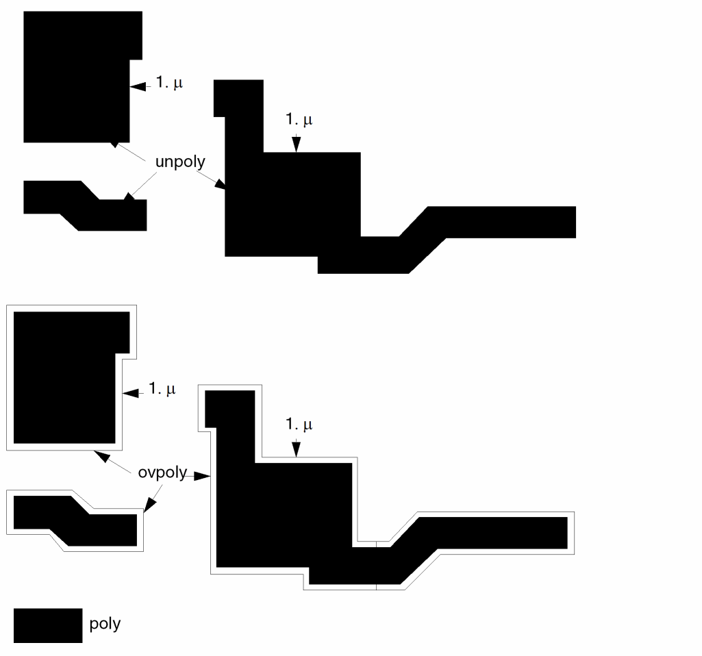
Example 6
After the logical operation, this example sizes the layer gate by 0.
AND dif poly gate
SIZE gate BY 0 OUTPUT gate 16
Example 7
SIZE[O] contact BY 2 drc3
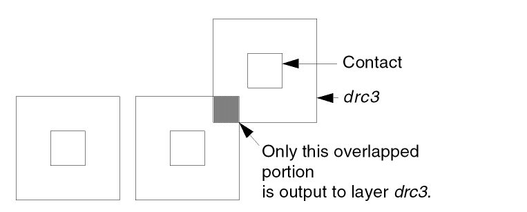
Example 8
When sizing layers from technologies that contain small geometries (2 microns or less), you can specify the SIZE-MIN-WIDTH command in the Description block. In this example, the SIZE command uses minimum polygon cut-line widths of 0.005 microns.
*DESCRIPTION
SIZE-MIN-WIDTH=0.005 mic
.
.
*END
*OPERATION
SIZE metal BY -.2 OUTPUT umetal 53
*END
If you want a 10X reticle and you are using an optical system, you must specify a minimum value of 0.4 microns for SIZE-MIN-WIDTH because 4 microns is the minimum flash width.
Example 9
The SIZE-MAX-VERTEX default value is 200 vertices. Use the default only with a CAD layout system that accepts PG-compatible polygon formats with less than 200 vertices. In this example, the maximum number of vertices is 50 when building polygons on layer nbur54.
*DESCRIPTION
SIZE-MAX-VERTEX=50
.
.
*END
*OPERATION
SIZE buried BY .2 OUTPUT nbur 54
*END
Example 10
SIZE[WN] poly BY 1 OUTPUT ovpoly 46 ; to output PG compatible
; ; polygon format data to
; ; a CAD system
SIZE met BY .25 omet
Example 11
This example checks a well region that contains a contact every 100 microns.
SIZE cont WITHIN well by 100 cont1
NOT well cont1 latcherr
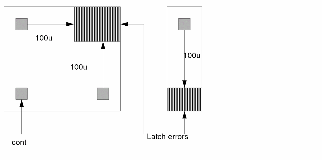
Example 12
;find metal 1 with width greater than 15 microns
SIZE metal1 DOWN-UP by 7.5 bigmet15
Example 13 - Optimizing the Rule Using the SIZE Command
In Dracula 4.81 and higher versions, you can speed up the run time by replacing
- Oversize or undersize sequence to “SIZE up-down” commands
- Undersize or oversize sequence to “SIZE down-up” commands
-
If you have set
optimize-rule=yesin your description block and if your statements in your rule file are as shown below:SIZE L1 by 0.1 T1 SIZE t1 by -0.1 L2
then PDRACULA will suggest to you to replace these above 2 statements by the following statement if you want to optimize your rule:SIZE L1 up-down by 0.1 L2
-
If you have set
optimize-rule=yesin your description block and if your statements in your rule file are as shown below:SIZE L1 by -0.1 T1 SIZE t1 by 0.1 L2
then PDRACULA will suggest to you to replace these above 2 statements by the following statement if you want to optimize your rule:SIZE L1 down-up by 0.1 L2
Example 14 -
SIZE L1 by <s>* TRUNCATE 1.41 L2
where <s> is the sizing distance.
This will size the following figure:
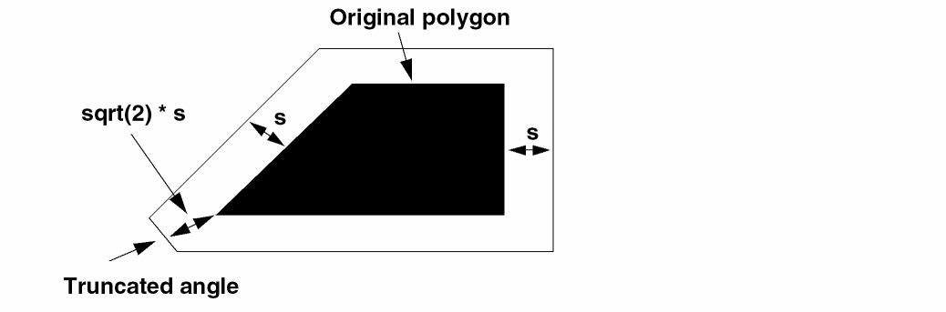
SNAP
SNAP{[P]} layer-a TO grid-value {trapfile]
Description
Snaps the coordinates of the geometry to a specified grid and outputs the result to another layer.
Arguments
Snaps the coordinates of the geometry to a specified grid in a polygon file. The default is to snap the coordinates of the geometry to a specified grid in a trapezoid file.
Input layer name. If P is specified, the input-layer must be a polygon file.
Grid to which to snap the layer. The value must be the multiple of the RESOLUTION specified in the Description block.
Output layer name. The trapfile can have up to seven alphanumeric characters and no special characters. The first character must be a letter. If P is not specified, the trapfile name must be specified.
All coordinates of the input-layer are snapped to the nearest grid. The middle point is snapped in the positive direction.
Example
*DESCRIPTION
RESOLUTION = 0.005 mic
*END
*OPERATION
SNAP YYPOLY TO 0.1 ZZPOLY
SIZE ZZPOLY BY 0.0 OUTPUT PPOLY 4
SNAP[P] PPOLY04 TO 0.1
SOFTCHK
SOFTCHKlower-layer{trapfile} OUTPUT[U]c-name l-num{d-num}
Description
Reports regions on a specified layer that connect to more than one node.
Arguments
Layer defined in SCONNECT that you are checking and from which you need to generate the soft connection violation outputs.
Name you designate as the output file to contain composite trapezoids. Before you do any operation on a trapfile, you need to either “OR” the layer with itself or “AND” the layer with the substrate layer.
Sends the results of the operation to an output cell.
Outputs an upper_layer file containing all geometries.
Outputs an upper_layer file containing the errors Dracula selects.
C-name is the name of the output cell and can have six alphanumeric characters or fewer and no special characters. L-num is the cell layer number determined by your CAD system. If your c-name is rule03 and
l-num is 5, the output cell name is rule0305.
Datatype number associated with the layer number (l-num) of the output cell. Use d-num for GDSII only. Values can range from 0 to 63.
If there is more than one connection, the soft connection check region is connected by only the contacts whose node number contains the most number of trapezoids among the node numbers of the multiple contacts. It is best to fix the violations before continuing the job.
All involved layers, except the specified layer, must have nodal information before any soft connection check can be made.
Soft connection violations are reported in the .ERC file. In addition, the U option generates a graphic output file. This file has the trapezoids on the layers connecting the upper_layer and lower_layer. The file name is as specified in OUTPUT but preceded by U.
Example
CONNECT-LAYER = NSUB PWELL PSD NSD POLY METAL MET2
.
.
.
CONNECT MET2 METAL BY VIA
CONNECT METAL POLY BY CONT
CONNECT METAL PSD BY CONT
CONNECT METAL NSD BY CONT
SCONNECT PSD PWELL BY CONT
SCONNECT NSD NSUB BY NCONT
.
.
.
SOFTCHK PWELL OUTPUT[U] DSOFT 50
SPFSELECT
SPFSELECT{[opt]} element{[type]}{REL val-a} {RANGE val-a val-b} {CORNER = n1} {OUTPUT c-name {l-num}} {&}
Description
Generates a detailed standard parasitic file (DSPF) for HPRE. For more information about the DSPF format, refer to
Argument definitions for the SPFSELECT command are the same as for the LPESELECT command except that you cannot specify a type if you specify a CAP element in your run file.
To generate a DSPF file according to DFII instance or net naming conventions, specify the SPF-MAP-FILE command in the Description block. This DSPF file can be used as an input to Cadence Central Delay Calculator (CDC) tools for timing analysis.
Checking Method
Arguments
|
Flags capacitances on all nodes, including power and ground nodes; if not specified, capacitances on power and ground nodes are not reported. |
|
|
Checks cross-coupling capacitance; if not specified, total loading is assumed. Dummy C’s and R’s are not output into the SPF file. |
|
|
Specifies that the original ground node names, rather than the default VSS node name, are used in the output SPICE file. This option should not be used with the N option. VSS is the default for composite and cell mode. In multiple-ground cases, if you want only one of them as ground node in the output SPICE file, the LPE-GROUND command now lets you specify a unique ground name. The LPE-GROUND command overwrites this SPFSELECT[G] command. |
|
|
Does not smash parallel transistors as one; for example, transistors of the same source, gate, drain (connected to the same nodes). Instead, these transistors are reported individually. |
|
|
Checks cross-coupling capacitance as a percentage of total loading. If you do not specify this option, a check is performed directly against val-a. Options C, P, and A are implemented to select only capacitors. |
|
|
Reports the area and perimeter of parasitic capacitors. The area is reported in place of the capacitance value. The perimeter is reported as a comment with the prefix PERI=. |
|
|
Schematic node names report preferred (from LOGLVS). For this S option, the schematic ground is used in flat mode. VSS is still used as the default for composite and cell mode. You can use the G option or LPE-GROUND to overwrite the default ground VSS. |
|
|
Does not comment out parasitic CAP and RES with terminals connected to power and ground nodes or power and ground subnodes in the DSPF output. This option takes effect whether you do or do not specify back annotation. This option is used together with Z option. Whenever you specify the Z option, resistors and capacitors extracted on power and ground nets are output in commented form. You can use the U option to uncomment them. |
|
|
Reports the transistor x and y coordinates in the LPESELECT listing file. |
|
|
Outputs resistors and capacitors extracted on power and ground nets in the DSPF file. You cannot use this DSPF as input to Cadence CDC. The Z option also outputs the instance name in front of power and group net names in the instance section of the DSPF file. |
Type code specified in the ELEMENT device command. If no type is specified, all ELEMENT types are invoked.
Specifies a one- or two-character code to denote the type of the element.
To group or smash different subtypes of capacitors, specify type as [new-subtype:subtype+subtype+...]. This syntax sums the capacitance values of multiple subtypes into a new subtype. The SPICE output file then contains all parasitic metal caps, all poly capacitors, and so forth, smashed into a new group subtype. The subtypes can have different parset numbers and must be defined by PARASITIC commands. You cannot use the S option when you group different subtypes.
Specifies one of the following:
Specifies element parameters, which must be greater than or equal to
val-a and less than or equal to val-b.
Specifies value for value-a or value-b, which can be floating point (maximum of 7 digits) or a floating-point number followed by an integer exponent (maximum 2 digits). When floating-point numbers are specified, the leading zeros are not counted in the 7-character restriction. The preprocessor rounds the value at the 7th digit. In scientific notation, the limit is 16 characters and is truncated at the 17th.
Effective MOS channel width/length calculation. You can specify CORNER as a positive or negative value. For a pulldown device (default = 0), for each 15-degree turn in a transistor channel, a 1/6 fraction of CORNER specified times length (L) is added or subtracted from a transistor default width (W). For a load-device, W is not changed and L is modified.
CORNER uses the same algorithm as WEFFECT in LPECHK.
Outputs SPICE listing to a file.
C-name and l-num are concatenated to make up the file name and the subcircuit name of the SPICE listing. C-name can have six alphanumeric characters. If l-num is not specified, only c-name is used. For example, if c-name = CKTNAM and l-num = 10, the output file name is CKTNAM10 and the subcircuit name is the same in the SPICE listing.
Indicates a conjunctive rule. This command can be used only with other LPESELECT commands.
For more information about ELEMENT MOS/DIO/CAP/BJT/RES, see Chapter 7, “Extracting Electrical Parameters (LPE).”
Example
SPFSELECT[S] RES[A] &
SPFSELECT[S] CAP OUTPUT SPF1
STAMP
STAMPstamped-layerBYstamping-layer{OUTPUT {[options]}c-name l-num{d-num}}
Description
The layer processing sequence and the interlayer contacts form electrical nodes. Dracula forms and uniquely labels each electrical node that results from the CONNECT-LAYER and CONNECT commands. This process is called stamping.
The STAMP command flags generated layers that are part of an electrical node but are not defined in the CONNECT command. Use this command after establishing the circuit connection. STAMP places the node labeling information from the stamping layer on the stamped layer. Stamping occurs only for stamped-layer polygons that overlap polygons in the stamping layer.
The STAMP command is not necessary for layers that result from the AND and NOT commands. Dracula automatically stamps layers produced with the AND and NOT commands. Dracula stamps the output layer with the node labeling of the first layer (layer-a).
Arguments
Name of a previously generated layer to stamp with the electrical node specification.
Name of a layer that contains the electrical node labeling information. This layer can result from a previous CONNECT or STAMP.
Generates an error file containing multiple-stamped geometries. The error output coordinates are also reported in the .LOG and .ERC files.
C-name is the name of the output cell and can have six alphanumeric characters or fewer and no special characters. L-num is the cell layer number determined by your CAD system. If your c-name is rule03 and
l-num is 5, the output cell name is rule0305.
Datatype number associated with the layer number (l-num) of the output cell. Use d-num for GDSII only. Values can range from 0 to 63.
Can be from among the following:
Example
CONNECT met poly BY cont
STAMP cont BY met ;met has node information
In the figure, numbers 12 and 60 are internal node numbers of layer met, and 0 represents either a no stamped node number or a conflicting node number.
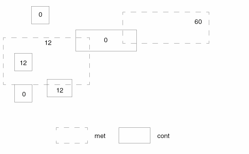
TRIANGLE
TRIANGLEinput-layersizeoutput-layer
Description
Creates an output file that contains four triangle shapes at four corners of input trapezoids.
Arguments
BULK layer defined in the SUBSTRATE command.
Length (in microns) of the legs of the triangles. If the length or width of the trapezoid is less than the specified size, Dracula does not generate the triangles for that trapezoid.
Output layer for the triangles.
Example
*OPERATION
.
TRIANGLE BULK 5 TRIBULK
*END
This example results in the following:
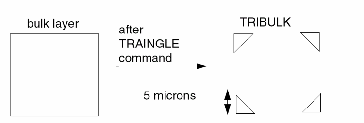
WIDTH
WIDTH{[option1]} layer-a{&layer-a}[option2] LT/LE/RANGE/SELLT/SELLE/ SELGT/SELGE/SELRA/ GT/GE/EQ/SELEQ/SELNE n1 {n2} ANGLE = angle-opt {trapfile} {OUTPUT c-name l-num {d-num}} {&}
WIDTH{[option1]} layer-a RECT = n3 BY n4 {trapfile} {OUTPUT c-name l-num {d-num}}
Description
Checks the dimensions between inside edges of polygons on the input layer.
Shell environment variables
-
setenv SPAC_LISTERR_DIGIT [ 2 | 3 ]
Use this environment variable to set number of digits after the decimal point for EXT/ENC/WIDTH/INT log report.
Checking Method
Flat, cell, hierarchical, composite.
Arguments
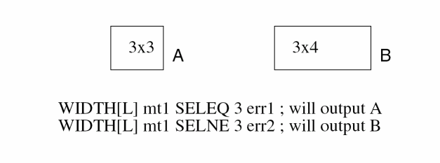

Renames (conjunctive-rename) the layer containing the error flags. The original layer name is then restored to the original layer. No spaces are allowed between the layer-a and &layer-a1 names, for example, poly&rpoly.
Measures between all nonconsecutive pairs of inside edges of the polygons on the input layer.
Compares the measurements against the limits you specify and flags violations.
Flags an error if the two segments are spaced less than n1 for LT or less than or equal to n1 for LE. Does not flag an error if the segments touch.
Flags an error if the two segments are spaced less than n2 and greater than n1. If you do not want acute-angle error flags, you must specify the RANGE measurement.
SELLT and SELLE output in trapezoid format those layer-a polygons that the program flags if you specify an LT n1 or an LE n1 and use the same options. Specify a trapfile name instead of using the OUTPUT statement.
SELGT outputs in trapezoid format the layer-a polygons that the program does not flag if you specify an LE measurement with the same options. SELGE has the same function as SELGT except that it works for an LT operation. You cannot use the OUTPUT statement with this option. Specify a trapfile name instead of using the OUTPUT statement.
SELRA outputs in trapezoid format those layer-a polygons that the program would flag if you specify a RANGE n1 n2 measurement and use the same options. Specify a trapfile name instead of using the OUTPUT statement.
Flags an error if the two segments are spaced greater than n1 for GT or greater than or equal to n1 for GE. Does not flag an error if the segments touch.
Flags an error if the two segments are spaced equal to n1 for EQ. Does not flag an error if the segments touch.
SELEQ output in trapezoid format those layer-a polygons that the program flags if you specify an EQ n1 and use the same options while SELNE outputs in trapezoid format those layer-a polygons that fail the EQ condition. Specify a trapfile name instead of using the OUTPUT statement.
Specifies the 45, non-45, 90, or non-90 degree angle to be checked. When you use this option, the C option for the ANGLE option is automatically invoked, and you cannot disable it.
Trapezoid file name. Use this option only with the R or R' option or with the SELLT, SELLE, SELGT, SELGE, SELRA operations.
Sends the results of the operation to an output cell.
Checks rectangle shapes that are exactly this size: n3xn4.
C-name is the name of the output cell and can have six alphanumeric characters or fewer and no special characters. L-num is the cell layer number determined by your CAD system. Id your c-name is rule03 and
l-num is 5, the output cell name is rule0305.
Datatype number associated with the layer number (l-num) of the output cell. Use d-num for GDSII only; values can range from 0 to 63.
Layer Options
Checks the original layer, not the layer generated by the previous operation in the conjunctive rule. Use this option only with a conjunctive rule and on a layer with error flags.
Example 1
ENC layer1 layer2 LT 1 outl1 &
WIDTH layer1[O] LT 2 OUTPUT err1 23
Example 2
WIDTH metal LT 5 OUTPUT drc07 92
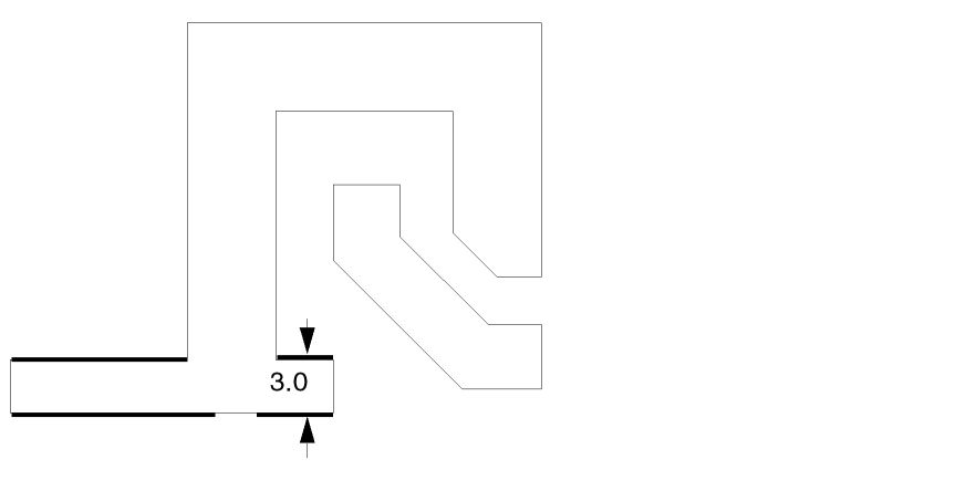
Example 3
This example checks for external metal spacing of 5.0 microns of metal lines that are 4.0 microns wide. These narrow metal lines must be spaced at 5.0 microns and not at 4.0 microns for wider busses.
WIDTH[PC] metal LE 4 &
EXT[PC] metal metal[O] LT 5 OUTPUT drc07 93
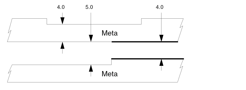
Example 4
WIDTH[PC] metal&meta E 4 &
EXT[PC] &meta metal LT 5 OUTPUT drc07 94
Also checks for external metal spacing as described in Example 2. Use the conjunctive-rename operation. This allows the &meta conjuncted layer to be used later in another DRC conjunctive check. Layer metal reverts to metal[O] at this point. Conjunctive-rename is optional and can save CPU resources.
Example 5
WIDTH met LT 3 output drc07 98
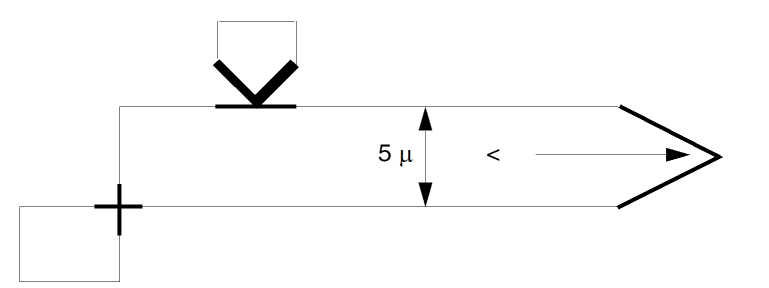
Example 6
This example checks for the width of circle metal contact (cmc) and produces no false errors.
WIDTH[C] cmc LT 5 drc07 90
Example 7
This example checks for metal contacts (mc) that are not 3 by n microns.
WIDTH[R] mc RANGE 2.99 3.01 mc3
NOT mc mc3 badmc OUTPUT drc07 91
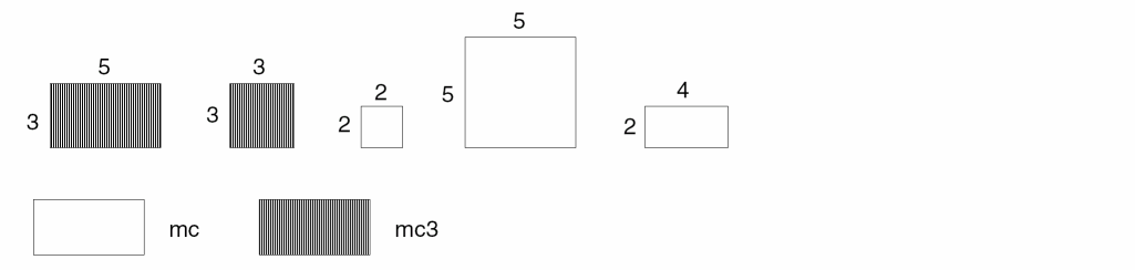
Example 8
The first three command lines check for transistor channel length of less than 3 microns. The fourth command checks for gate external spacing to contact (mc) in the direction of diffusion only. Touching is also an error.
This example renames the gate layer to &gwidth in the conjunctive-rename operation. This optional conjunct-rename operation saves a conjunctive command for the DRC check drc0796, thereby saving CPU resources.
AND poly diff gate
ENC[T] gate&gwidth poly LT .001 &
WIDTH[P] &gwidth LT 3 OUTPUT drc07 92
EXT[T] &gwidth mc LT 4 OUTPUT drc07 96
Example 9
This example outputs metal polygons that have widths greater than 10 microns only. Does not output widths less than or equal to 10 microns. The output layer is wmetal and is in trapezoid format.
WIDTH metal SELGT 10 wmetal
Example 10
This example outputs metal polygons that are 10 microns in width at some point and are output to layer metal10 in trapezoid format.
WIDTH metal SELRA 9.9 10.1 metal10
Example 11
This example outputs the contact in the 3 X 3 rectangle shape.
WIDTH[L] CONTACT SELEQ 3 OUTPUT ERR 01
XBOX
XBOX {[T]} {[F]} layer-a OUTPUT c-name l-num {d-num}
Description
Checks for composite geometries in the specified layer that overlap or touch cell boxes (Hcell boundaries). Use the XBOX command to gather information about an HLVS operation.
Checking Method
Arguments
Indicates that touching is a violation.
Uses inner boundaries for framed Hcells, instead of Hcell boundaries, to check overlapping or touching.
Sends the results to an output cell.
C-name is the name of the output cell and can have six alphanumeric characters or fewer and no special characters. L-num is the cell layer number determined by your CAD system. If your c-name is rule03 and
l-num is 5, the output cell name is rule0305.
Datatype number associated with the layer number (l-num) of the output cell. Use d-num for GDSII only. Values can range from 0 to 63.
Example
XBOX poly OUTPUT xpoly 55
XBOX[T] metal OUTPUT xmet 10
XBOX[TF] poly OUTPUT xpoly 51
XCELL
XCELLlayer-a layer-bOUTPUTc-name l-num{d-num}
Description
Checks for geometries from the composite plane of layer-a or layer-b that overlap geometries in the Hcells from layer-a or layer-b.
Use this command prior to an HLVS run to check for any device formation caused by overlapping areas of Hcells or by composite geometries that overlap Hcells. These devices are also checked by XDEVICE. Devices can be formed only by geometries that are solely from the composite or solely from within an Hcell. (The BASE-LAYER command is an exception to this rule.)
Checking Method
Arguments
Outputs the results of the operation in the form of an output cell, where:
C-name is the name of the output cell and can have six alphanumeric characters or fewer and no special characters. L-num is the cell layer number determined by your CAD system. If your c-name is rule03 and
l-num is 5, the output cell name is rule0305.
Datatype number associated with the layer number (l-num) of the output cell. Use d-num for GDSII only. Values can range from 0 to 63.
Example
XCELL poly diff OUTPUT badgat 10
XDEVICE
XDEVICEelement[subtype] OUTPUTC-name l-num{d-num}
Description
Outputs devices formed by composite-to-cell or cell-to-cell interactions in a composite mode HLVS/HLPE/HERC run. These devices are extra devices that are not present in the schematics. The LVS report lists these devices, but they are not used in LVS matching nor reported in the HLPE output file.
Specify only one XDEVICE command for each ELEMENT declaration. Dracula creates .ENC files for every layer. These .ENC files store information about the area between the cell plane and composite plane.
Arguments
Sends the results to an output cell.
C-name is the name of the output cell and can have six alphanumeric characters or fewer and no special characters. L-num is the cell layer number determined by your CAD system. If your c-name is rule03 and
l-num is 5, the output cell name is rule0305.
Datatype number associated with the layer number (l-num) of the output cell. Use d-num for GDSII only. Values can range from 0 to 63.
Example
This example outputs the composite-to-cell and cell-to-cell devices for MOS[P] to error cell ILLP10 and those for MOS[N] to ILLN11.
*OPERATION
ELEMENT MOS[P] PGATE POLY PSRCDRN NSUB
ELEMENT MOS[N] NGATE POLY NSRCDRN PWELL
XDEVICE MOS[P] OUTPUT ILLP 10
XDEVICE MOS[N] OUTPUT ILLN 11
LVSCHK[C]
*END
Dracula checks, and flags with x and y coordinates, devices formed by cell-to-cell or cell-to-composite interactions in the LVS report file. By the definition of an Hcell, these devices do not exist in the schematics. They are flagged as extra layout devices. The report format is as follows:
*********** XDEVICE SUMMARY REPORT ***********
EXTRA COMPOSITE/CELL OR CELL/CELL DEVICES IN LAYER ILLN ILLN X= 5521.50, Y= 4396.50 ILLN X= 5540.50, Y= 4396.50
Dracula lists only the first 100 occurrences in the LVS report. They are listed whether or not you specified an XDEVICE. If you want an output layer for these devices, use the XDEVICE command. The output layer is a flat layer and all devices are output.
XOR
XOR {[D{n}]} layer-a layer-b trapfile {OUTPUT c-name l-num {d-num}}
Description
Creates a new layer from two other layers. The new layer consists of the total region of both layers minus the region shared by both layers.
Database partition functions were added for the SELECT, SIZE, and LOGICAL commands. These enhancements resolve capacity limitation issues with Dracula. This allows you to partition input layers of these functions into blocks. When you run Distributed Dracula, each block (pair) can be assigned to one processor. Specify a value between 2-10 inclusive following ‘D’ to indicate the number of partitions desired. The default value of ‘D’ is 4 if the value is omitted.
Arguments
Turn on the database partition feature
Number of blocks to be partitioned into
Trapezoid file created by the logical operation. The trapfile name can have up to seven characters and no special characters. A-Z and 0-9 are permitted, but the first character must be a letter.
Sends the results of the operation to an output cell.
C-name is the name of the output cell and can have six alphanumeric characters or fewer and no special characters. L-num is the cell layer number determined by your CAD system. If your c-name is rule03 and
l-num is 5, the output cell name is rule0305.
Datatype number associated with the layer number (l-num) of the output cell. Use d-num for GDSII only. Values can range from 0 to 63.
Example
The following example shows a database comparison between layers that are supposed to be identically digitized.
XOR diffa diffb err1
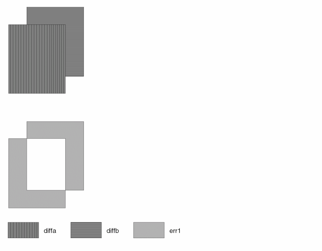
XVIA
XVIAlayer-aOUTPUTC-name l-num{d-num}
Description
Checks for a contact layer that is not covered by a related conductor layer in either the composite plane or in the Hcells. You must specify the contact layer and related connect layers in a prior CONNECT command.
Checking Method
Arguments
Layer containing the contacts to be checked.
Sends the results to an output cell.
C-name is the name of the output cell and can have six alphanumeric characters or fewer and no special characters. L-num is the cell layer number determined by your CAD system. If your c-name is rule03 and
l-num is 5, the output cell name is rule0305.
Datatype number associated with the layer number (l-num) of the output cell. Use d-num for GDSII only; values can range from 0 to 63.
Use this command to detect floating contacts that are not found otherwise and that are not allowed in HLVS runs.
Example
XVIA contact OUTPUT uncont 10
XVIA via OUTPUT unvia 44
Return to top