Model Equations
Effective Oxide Thickness, Channel Length and Channel Width
Gate Dielectric Model
The finite chargelayer thickness cannot be ignored when the gate oxide thickness is vigorously scaled down. There are two ways in BSIM4 for modeling this effect in both IV and CV, which can be selected by mtrlmod. When mtrlmod=0 (for SiO2 gate) , the input parameters includes toxe, toxp and dtox. When mtrlmod=1 (for high-k dielectric gate), the input parameters includes eot, weffeot, leffeot, tempeot and vddeot. toxe is equal to eot, and toxp could be calculated by the input parameters.
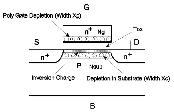
Poly-Silicon Gate Depletion
Charge distribution in a MOSFET with the poly gate depletion effect is shown in the following figure. The device is in the strong inversion region.
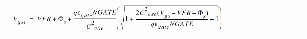
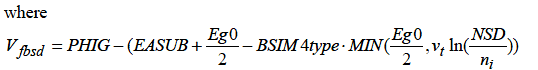
The effective gate voltage Vgse is
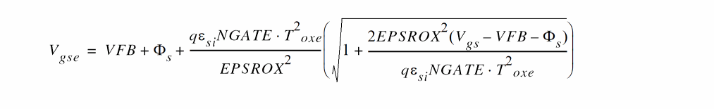
For mtrlmod =1(the non-silicon channel or high -k gate insulator
Effective Channel Length and Width
WINT represents the traditional manner from which "delta W" is extracted (from the intercept of straight lines on a 1/Rds~Wdrawn plot). The parameters DWG and DWB are used to account for the contribution of both gate and substrate bias effects. For dL, LINT represents the traditional manner from which "delta L" is extracted from the intercept of lines on a Rds~Ldrawn plot.
The remaining terms in dW and dL are provided for your convenience. They are meant to allow you to model each parameter as a function of Wdrawn, Ldrawn, and their product term. By default, the above geometrical dependencies for dW and dL are turned off.
MOSFET capacitances can be divided into intrinsic and extrinsic components. The intrinsic capacitance is associated with the region between the metallurgical source and drain junction, which is defined by the effective length (Lactive) and width (Wactive) when the gate to source/drain regions are under flat-band condition. Lactive and Wactive are defined as
The meanings of DWC and DLC are different from those of WINT and LINT in the I-V model. Unlike the case of I-V, these dimensions are bias-dependent. The parameter δLeff is equal to the source/drain to gate overlap length plus the difference between drawn and actual POLY CD due to processing (gate patterning, etching, and oxidation) on one side.
The effective channel length Leff for the I-V model does not necessarily carry a physical meaning. It is just a parameter used in the I-V formulation. This Leff is therefore sensitive to the I-V equations and also to the conduction characteristics of the LDD region relative to the channel region. A device with a large Leff and a small parasitic resistance can have a similar current drive as another with a smaller Leff but larger Rds.
The Lactive parameter extracted from capacitance is a closer representation of the metallurgical junction length (physical length). Due to the graded source/drain junction profile, the source to drain length can have a strong bias dependence. Lactive is measured at flat-band voltage between gate to source/drain. If DWC, DLC and the length/width dependence parameters (LLC, LWC, LWLC, WLC, WWC and WWLC) are not specified in technology files, BSIM4 assumes that the DC bias-independent Leff and Weff will be used for the capacitance models, and DWC, DLC, LLC, LWC, LWLC, WLC, WWC, and WWLC will be set to the values of their DC counterparts.
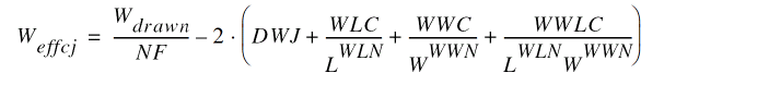
BSIM4 uses the effective source/drain diffusion width Weffcj for modeling parasitics, such as source/drain resistance, gate electrode resistance, and gate induced drain leakage (GIDL) current. Weffcj is defined as:
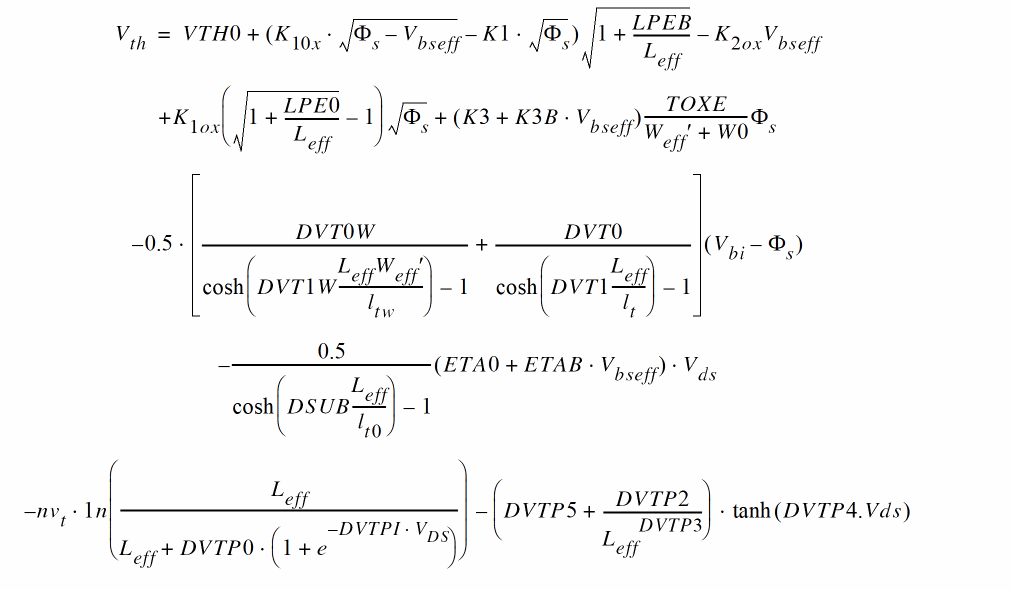
Threshold Voltage Model
Considering non-uniform doping, short-channel effect, DIBL effect, and narrow-width effect, the complete Vth model is:
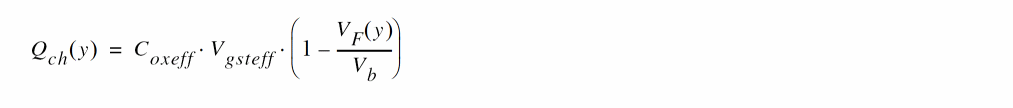
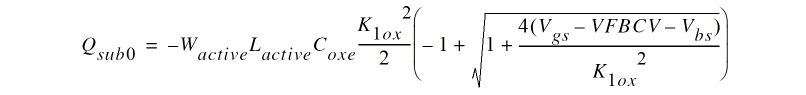
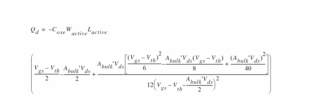
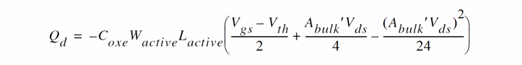
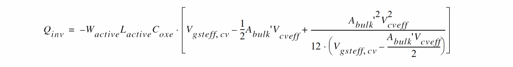
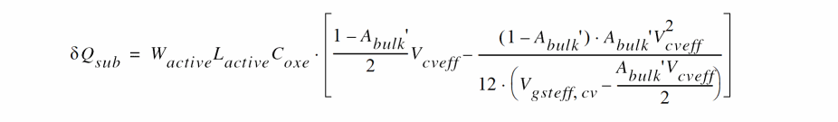
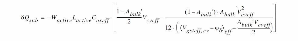
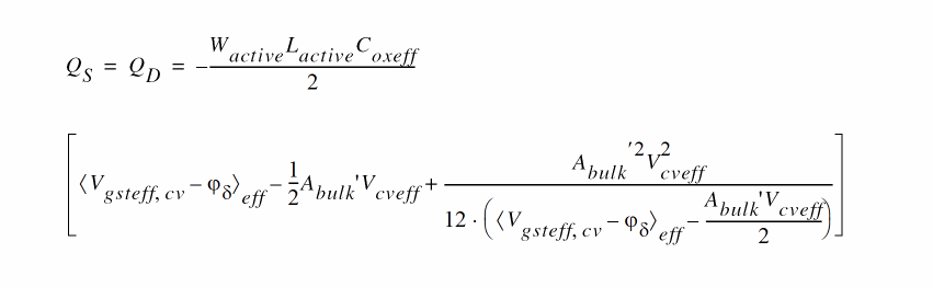
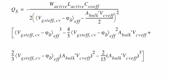
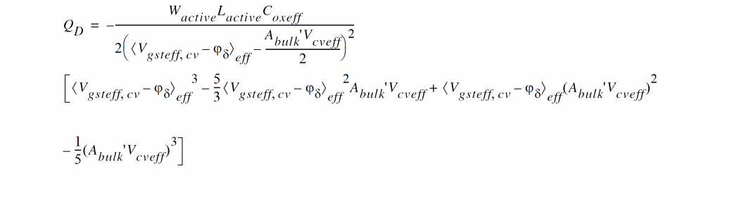
Channel Charge and Subthreshold Swing Models
A unified expression for channel charge from subthreshold to strong inversion regions is
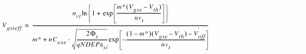
In the above equation, Vgsteff (the effective Vgst(Vgse-Vth)) used to describe the channel charge densities from subthreshold to strong inversion is modeled by:
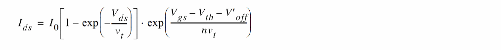
The drain current equation in the subthreshold region can be expressed as:

Gate Direct Tunneling Current Model
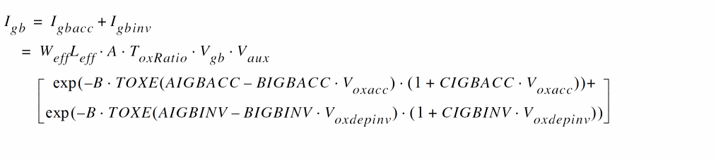
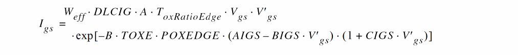
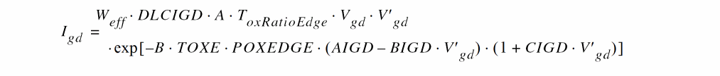
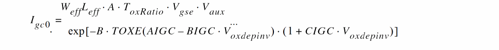
In BSIM4, the gate tunneling current components include the tunneling current between gate and substrate (Igb), and the current between gate and channel (Igc), which is partitioned between the source and drain terminals by Igc = Igcs + Igcd. The third component happens between gate and source/drain diffusion regions (Igs and Igd). Following figure shows the schematic gate tunneling current flows.
Igc, Igs, and Igd are turned on when igcmod = 1, 2; Igb is turned on when igbmod = 1; no gate tunneling currents are modeled when igcmod = 0. Vt (= kT/q) is replaced by Vtnom(=kTnom/q) when tempmod = 2. The gate tunneling current components are expressed as following:


Drain Current Model
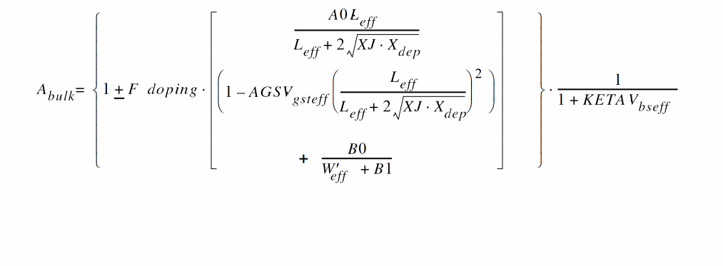
Bulk Charge Effect
The bulk charge effect caused by non-zero Vds is modeled as

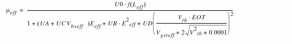
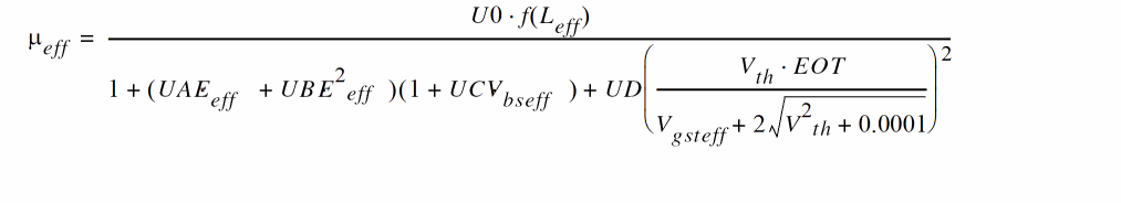
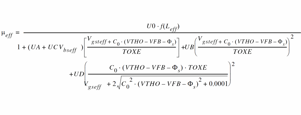
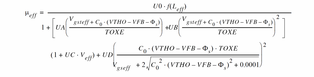
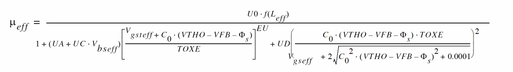
Mobility Model
Several mobility models are provided in BSIM4. For mtrlmod = 0, mobmod = 0 and 1 models are from BSIM3v3.2.2, mobmod = 2 is a universal mobility model, which is more accurate and suitable. For mtrlmod = 1, a new expression of the vertical field in channel is adopted (introduced by BSIM4.6.1). The mobility model is modified as following:
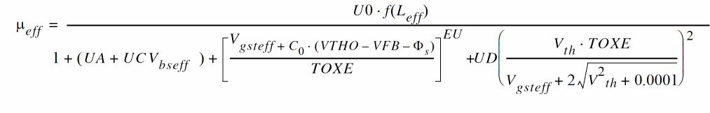
mobmod=3 for high k/metal gate structure (introduced by BSIM4..2):
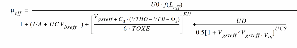
BSIM4.80 introduces three new mobility models, mobmod=4, mobmod=5, and mobmod=6 as modified versions of mobmod=0, mobmod=1, and mobmod=2 respectively.
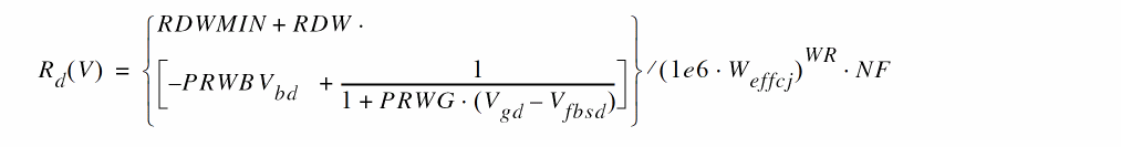
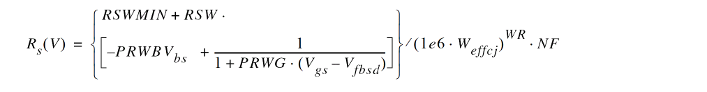
Bias-Dependant Source/Drain-Resistance Model
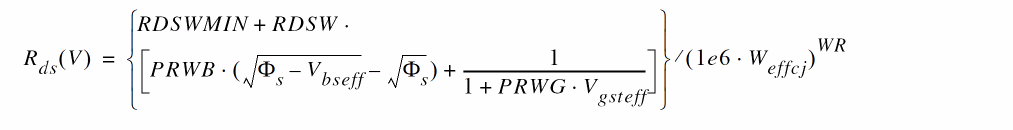
rdsMod=1 (External Rd(V) and Rs(V)
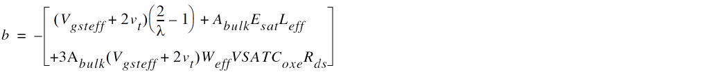
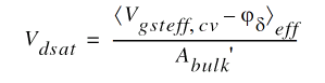
Saturation Voltage Vdsat


Drain Current
Considering only the channel current, the I-V curve can be divided into two parts: the linear region and the saturation region. In the linear region, carrier velocity is not saturated and the drain current has a strong dependence on the drain voltage. In the saturation region, several physical mechanisms affect the output resistance: channel length modulation (CLM), drain-induced barrier lowering (DIBL), and the substrate current induced body effect (SCBE). These mechanisms all affect the output resistance in the saturation range, but each of them dominates in a specific region. The channel current equation for both linear and saturation regions is:
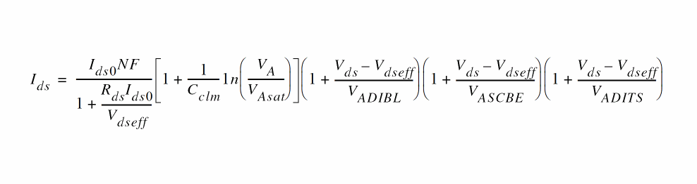
where NF is the number of device fingers, and Early voltage.
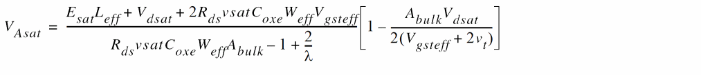
The Early voltage at Vds = Vdsat is
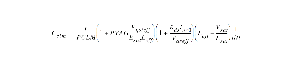
The Early voltage due to CLM effect is
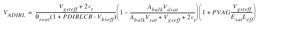
The Early voltage due to DIBL effect is
The Early voltage due to SCBE effect is

The Early voltage due to Drain-Induced Threshold Shift (DITS) by pocket implant is

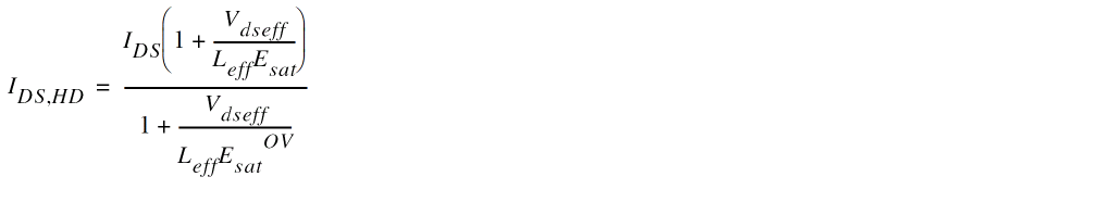
Velocity Overshoot and Source End Velocity Limit Model
In the deep-submicron region, the velocity overshoot and source end velocity limit model should be used. The unified current expression with velocity saturation, velocity overshoot and source velocity limit is:
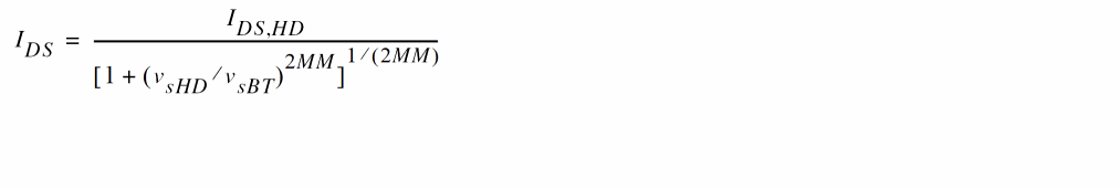
where the current including the velocity overshoot effect is:
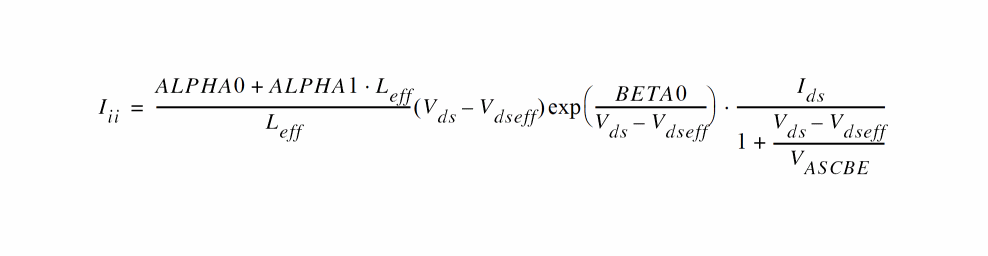
Body Current Model
Isub Model
When the electrical field near the drain is large (> 0.1MV/cm), some electrons coming from the source (in the case of NMOSFETs) will be energetic (hot) enough to cause impact ionization. This will generate electron-hole pairs when these energetic electrons collide with silicon atoms. The substrate current Isub thus created during impact ionization will increase exponentially with the drain voltage. A well known Isub model is:

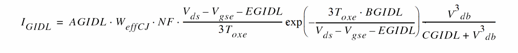
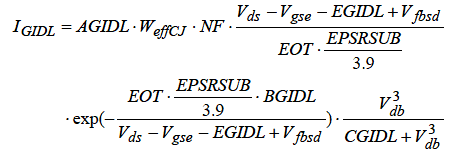
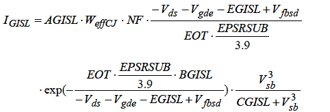
In addition to the junction diode current and gate-to-body tunneling current, the substrate terminal current consists of the substrate current due to impact ionization (Iii), and gate-induced drain leakage and source leakage currents (IGIDL and IGISL).

Capacitance Model
The following table displays the BSIM4 capacitance model options:
|
|
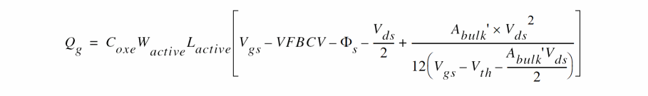
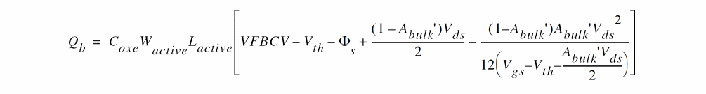
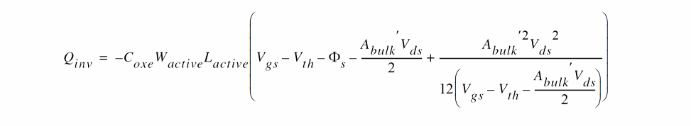
Intrinsic Capacitance Modeling
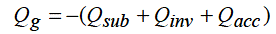
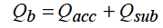
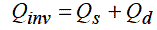
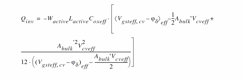
The relationship of terminal charges (Qg, Qb, Qs, and Qd) and the channel charge Qinv, accumulation charge Qacc and substrate depletion charge Qsub are:
All capacitances are derived from the charges to ensure charge conservation. Since there are four terminals, there are a total of 16 components. For each component:
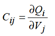
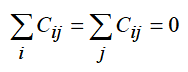
where i and j denote the transistor terminals. Cij satisfies
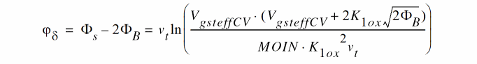
A new threshold voltage definition is introduced to improve the fitting in subthreshold region. Setting cvchargemod = 1 activates the new Vgsteff, CV calculation which is similar to the Vgsteff formulation in the I-V model. Setting cvchargemod = 0 is corresponding to long-channel charge model which assumes a constant mobility with no velocity saturation.
Intrinsic capacitance model equations
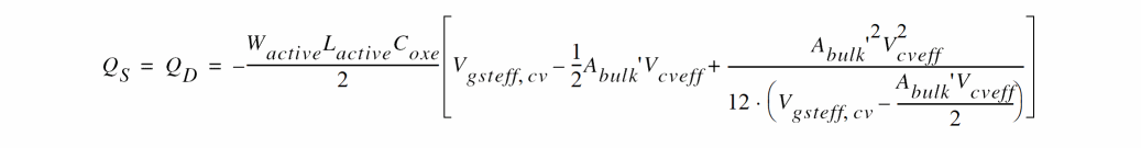
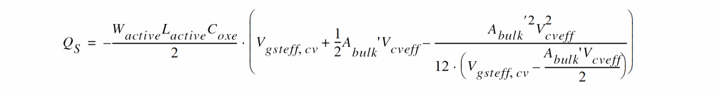
For capmod=0
40/60 Channel-Charge Partition
0/100 Channel-Charge Partition
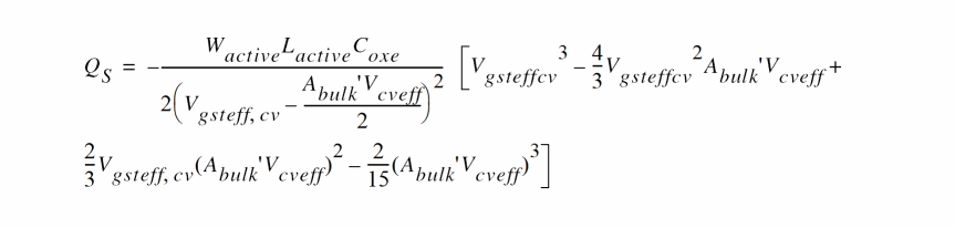
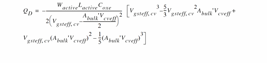
For capmod=1

40/60 Channel-Charge Partition
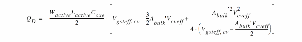
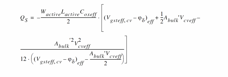
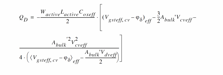
For capmod = 2
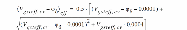
When updatelevel=1, a smooth function is applied when calculating (Vgsteff, cv- psidelta)eff to improve convergence behavior of the model.

When updatelevel=1, or version=4.5,
Intrinsic Capacitances (with Body Bias and DIBL)
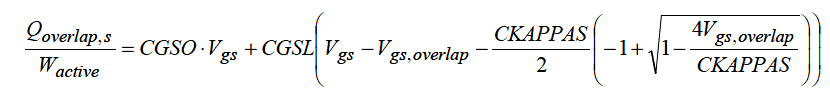
Overlap Capacitance Models
capmod=0, Bias-independent overlap capacitance model


capmod 1 and 2, Bias dependent overlap capacitance model


High Speed/RF Models
Charge-deficit Nonquasi-static (NQS) Model
BSIM4 uses two separate model selectors to turn on or off the charge-deficit NQS model in transient simulation (using trnqsMod) and AC simulation (using acnqsMod). The AC NQS model does not require the internal NQS charge node that is needed for the transient NQS model. The transient and AC NQS models are developed from the same fundamental physics: the channel/gate charge response to the external signal are relaxation-time ![]() dependent and the transcapacitances and transconductances (such as Gm) for AC analysis can therefore be expressed as functions for
dependent and the transcapacitances and transconductances (such as Gm) for AC analysis can therefore be expressed as functions for ![]() .
.
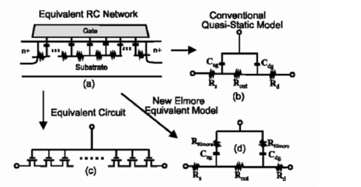
MOSGFET channel region is analogous to a bias-dependent RC distributed transmission line as shown section "a" of the figure below. In the Quasi-Static (QS) approach, the gate capacitor node is lumped with the external source and drain nodes as shown in section "b" of the figure below. This ignores the finite time for the channel charge to build-up. One way to capture the NQS effect is to represent the channel with n transistors in series as shown in section "c" of the figure below, but it comes at the expense of simulation time. The BSIM4 charge-deficit NQS model uses Elmore equivalent circuit to model channel charge build-up as shown in section "d" of the figure below.
The Transient Model
The transient charge-deficit NQS model can be turned on by setting trnqsMod = 1 and off by setting trnqsMod = 0.
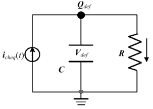
The figure below shows the RC subcircuit of charge deficit NQS model for transient simulation. An internal node, Qdef(t), is created to keep track of the amount of deficit/surplus channel charge necessary to reach equilibrium. The resistance R is determined from the RC time constant ![]() . The current source icheq(t) represents the equilibrium channel charging effect. The capacitor C is the value of Cfact (with a typical value of 1 x 10⁻⁹ Farad) to improve simulation accuracy. Qdef now becomes:
. The current source icheq(t) represents the equilibrium channel charging effect. The capacitor C is the value of Cfact (with a typical value of 1 x 10⁻⁹ Farad) to improve simulation accuracy. Qdef now becomes:
Considering both the transport and charging component, the total current related to the terminals D, G, and S can be written as:
Based on the relaxation time approach, the terminal charge and corresponding charging current are modeled by
where D,G,Sxpart are charge deficit NQS channel charge partitioning numbers for terminals D, G, and S; Dxpart + Sxpart = 1 and Gxpart = -1.
The transit time ![]() is equal to the product of Rii and WeffLeffCoxe, where Rii is the intrinsic-input resistance given by
is equal to the product of Rii and WeffLeffCoxe, where Rii is the intrinsic-input resistance given by
where Coxeff is the effective gate dielectric capacitance calculated from the DC model.
The AC Mode
The small-signal AC charge-deficit NQS model can be turned on by setting acnqsMod = 1 and off by setting acnqsMod = 0.
For small signals in the frequency domain, Qch(t) can be transformed into:
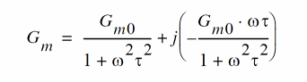
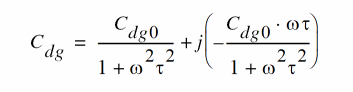
where ![]() is the angular frequency. It can be shown that the transcapacitances Cgi, Csi, and Cdi (i stands for any of the G, D, S, and B terminals of the device) and the channel transconductances Gm, Gds, and Gmbs all become complex quantities. For example, now Gm has the form of:
is the angular frequency. It can be shown that the transcapacitances Cgi, Csi, and Cdi (i stands for any of the G, D, S, and B terminals of the device) and the channel transconductances Gm, Gds, and Gmbs all become complex quantities. For example, now Gm has the form of:
The quantities above with sub "0" are known from OP (Operating Point) analysis.
Gate Electrode and Intrinsic-Input Resistance (IIR) Model
BSIM4 provides four options for modeling gate electrode resistance (bias-independent) and intrinsic-input resistance (IIR, bias-dependent). The IIR model considers the relaxation-time effect due to the distributive RC nature of the channel region, and therefore describes the first-order non-quasi-static effect. Thus, the IIR model should not be used together with the charge-deficit NQS model. The model selector rgateMod is used to choose different options.
rgateMod = 0 (zero-resistance)
In this case, no gate resistance is generated.
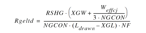
rgateMod = 1 (constant-resistance)
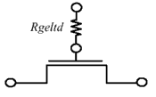
In this case, only the electrode gate resistance (bias-dependent) is generated by adding an internal gate node. Rgeltd is given by
rgateMod = 2 (IIR model with variable resistance)
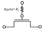
In this case, the gate resistance is the sum of the electrode gate resistance and the intrinsic-input resistance Rii. An internal gate node will be generated. trnqsMod = 0 (default) and acnqsMod = 0 (default) should be selected for this case.
rgateMod = 3 (IIR model with two nodes)
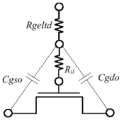
In this case, the gate electrode resistance given is in series with the intrinsic-input resistance Rii through two internal gate nodes, so that the overlap capacitance current will not pass through the intrinsic-input resistance. trnqsMod = 0 (default) and acnqsMod = 0 (default) should be selected for this case.
Substrate Resistance Network
For CMOS RF circuit simulation, it is essential to consider the high frequency coupling through the substrate. BSIM4 offers a flexible built-in substrate resistance network. This network is constructed so that little simulation efficiency penalty will result.
Model Selector and Topology
The model selector rbodyMod can be used to turn on or turn off the resistance network.
No substrate resistance network is generated at all.
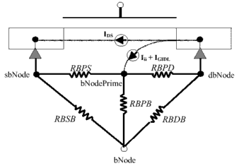
All five resistances in the substrate network as shown schematically below are present simultaneously.
A minimum conductance, GBMIN, is introduced in parallel with each resistance to prevent infinite resistance values which would otherwise cause poor convergence. In the following figure, GBMIN is merged into each resistance to simplify the representation of the model topology.
Noise Models
The following noise sources in MOSFETs are modeled in BSIM4 for noise analysis: flicker noise (also known as 1/f noise), channel thermal noise and induced gate noise and their correlation, thermal noise due to physical resistances such as the source/ drain, gate electrode, and substrate resistances, and shot noise due to the gate dielectric tunneling current.
Flicker Noise Models
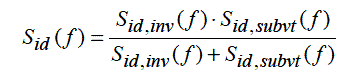
BSIM4 provides two flicker noise models: simple model and unified physical model (default model). They can be selected by fnoimod. Both modes come from BSIM3v3, but there are many improvements in unified physical model.
fnoiMod = 0 (simple model)
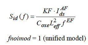
The total flicker noise density is:
The noise density in the inversion region is:
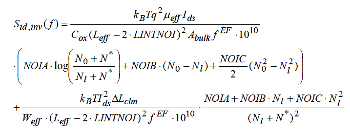
lintmoi is an offset to the length reduction parameter (lint) for flicker noise, which is introduced by BSIM4.4.
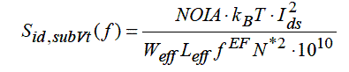
The noise density in the subthreshold region is:
Channel Thermal Noise
BSIM4 provides two channel thermal noise models: charge-based model (default model) and the holistic model. They can be selected by tnoimod. The schematic for BSIM4 channel thermal noise modeling is shown as following:
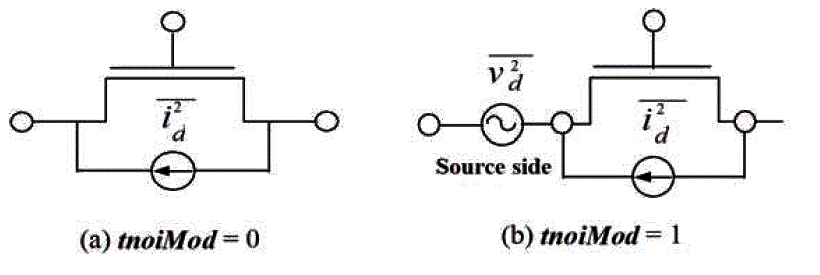
tnoiMod = 0 (charge-based)
Charge-based model is similar to that used in BSIM3v3.2. The noise current is given by:
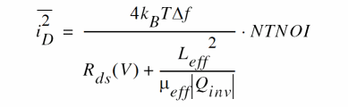
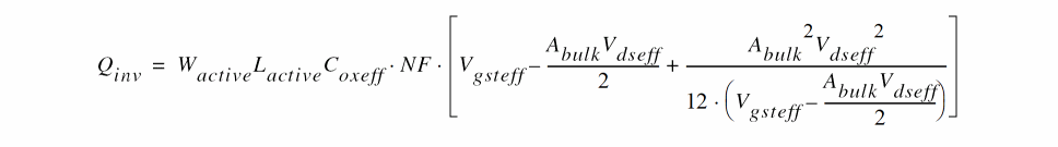
tnoiMod = 1 (holistic)
In this thermal noise model, all the short-channel effects and velocity saturation effect incorporated in the IV model are automatically included, hence the name “holistic thermal noise model”. In addition, the amplification of the channel thermal noise through Gm and Gmbs as well as the induced-gate noise with partial correlation to the channel thermal noise are all captured in the new “noise partition” model.
The noise voltage source partitioned to the source side is given by
The noise current source put in the channel region with gate and body amplification is given by:

Asymmetric MOS Junction Diode Models
Junction Diode IV Model
In BSIM4, there are three junction diode IV models. When the IV model selector dioMod is set to 0 ("resistance free"), the diode IV is modeled as resistance-free with or without breakdown depending on the parameter values of XJBVS or XJBVD. When dioMod is set to 1 ("breakdown-free"), the diode is modeled in the same way as in BSIM3v3 with current-limiting feature in the forward-bias region through the limiting current parameters IJTHSFWD or IJTHDFWD; diode breakdown is not modeled for dioMod = 1 and XJBVS, XJBVD, BVS, and BVD parameters all have no effect. When dioMod is set to 2 ("resistance-and-breakdown"), BSIM4 models the diode breakdown with current limiting in both forward and reverse operations. In general, setting dioMod to 1 produces fast convergence.
diomod=0 is not recommended. Use diomod=2 instead.Source/Body Junction Diode
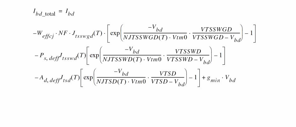
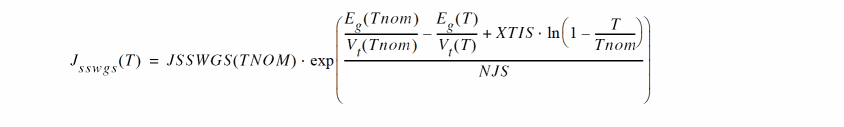
where Isbs is the total saturation current consisting of the components through the gate-edge (Jsswgs) and isolation-edge sidewalls (Jssws) and the bottom junction (Jss).
In the above equation, if XJBVS = 0, no breakdown will be modeled. If XJBVS < 0.0, it is reset to 1.0.
The exponential IV term is linearized at the limiting current IJTHSFWD in the forward-bias model only.
dioMod = 2 (resistance-and-breakdown)
Diode breakdown is always modeled. The exponential term is linearized at both the limiting current IJTHSFWD in the forward-bias mode and the limiting current IJTHSREV in the reverse-bias mode.
for dioMod = 2, if XJBVS <= 0.0, it is reset to 1.0.
Drain/Body Junction Diode
The drain-side diode has the same system of equations as those for the source-side diode, but with a separate set of model parameters.
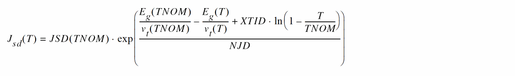
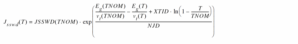
where Isbd is the total saturation current consisting of the components through the gate-edge (Jsswgd) and isolation-edge sidewalls (Jsswd) and the bottom junction (Jsd),
In the above equation, when XJBVD = 0, no breakdown is modeled. If XJBVD < 0.0, it is reset to 1.0.
No breakdown is modeled. The exponential IV term is linearized at the limiting current IJTHSFWD in the forward-bias model only.
dioMod = 2 (resistance-and-breakdown)
Diode breakdown is always modeled. The exponential term is linearized at both the limiting current IJTHSFWD in the forward-bias mode and the limiting current IJTHSFWD in the reverse-bias mode.
For dioMod = 2, if XJBVD <= 0.0, it is reset to 1.0.
Total Junction Source/Drain Diode Including Tunneling
Total diode current including the carrier recombination and trap-assisted tunneling current in the space-charge region is modeled by:

Junction Diode CV Model
Source and drain junction capacitances consist of three components: the bottom junction capacitance, sidewall junction capacitance along the isolation edge, and sidewall junction capacitance along the gate edge. An analogous set of equations are used for both sides but each side has a separate set of model parameters.
Source/Body Junction Diode
where Cjbs is the unit-area bottom S/B junction capacitance, Cjbsws is the unit-length S/B junction sidewall capacitance along the isolation edge, and Cjbswgs is the unit-length S/B junction sidewall capacitance along the gate edge.
Cjbs
Cjbsws
Cjbsws
Drain/Body Junction Diode
where Cjbd is the unit-area bottom D/B junction capacitance, Cjbswd is the unit-length D/B junction sidewall capacitance along the isolation edge, and Cjbswgd is the unit-length D/B junction sidewall capacitance along the gate edge.
Cjbd
Cjbdsw
Cjbdswg
Layout Dependent Parasitics Models
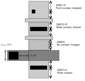
The following figure shows the geometry definition for various source/drain connections and source/drain/gate contacts. The layout parameters shown in this figure will be used to calculate resistances and source/drain perimeters and areas.
Effective Junction Perimeter and Area
The source-side case is illustrated below. The same approach is used for the drain side. The effective junction perimeter is calculated by:
Pseff computed from NF, DWJ, geoMod, DMCG, DMCI, DMDG, DMCGT, and MIN.
The effective junction area is calculated by:
Aseff computed from NF, DWJ, geoMod, DMCG, DMCI, DMDG, DMCGT, and MIN.
In the above, Pseff and Aseff will be used to calculate junction diode IV and CV. Pseff does not include the gate-edge perimeter.
| geoMod | End source | End drain | Note |
|---|---|---|---|
Temperature Effects Models
Accurate modeling of the temperature effects on MOSFET characteristics is important to predict circuit behavior over a range of operating temperatures (T). The operating temperature might be different from the nominal temperature (TNOM) at which the BSIM4 model parameters are extracted.
Temperature Dependence of Threshold Voltage
The temperature dependence of Vth is modeled by:
Temperature Dependence of Mobility
Temperature Dependence of Saturation Velocity
Temperature Dependence of LDD Resistance
rdsMod = 0 (internal source/drain LDD resistance)
rdsMod = 1 (external source/drain LDD resistance)
Temperature Dependence of Junction Diode IV
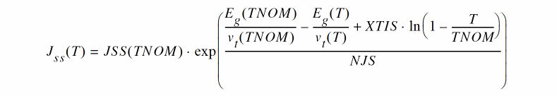
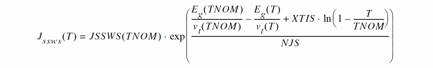
Trap-assisted Tunneling and Recombination Current
Temperature Dependence of Junction Diode CV
The temperature dependences of zero-bias unit-length/area junction capacitances on the source side are modeled by
The temperature dependences of the built-in potentials on the source side are modeled by
Stress Effects Models
BSIM4 considers the influence of stress on mobility, velocity saturation, threshold voltage, body effect, and DIBL effect. The following diagram displays the LOD instance geometry parameters SA and SB.
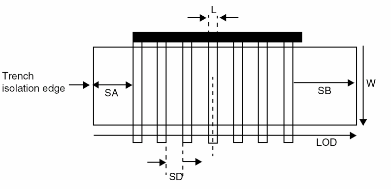
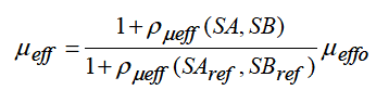
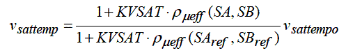


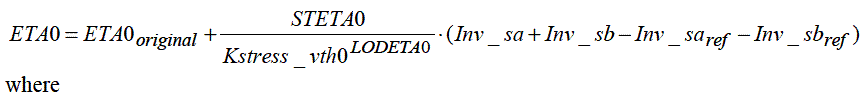
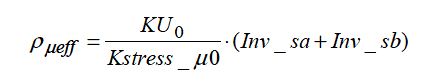
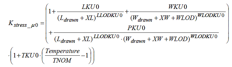
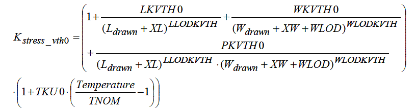
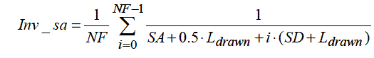
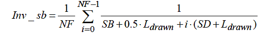
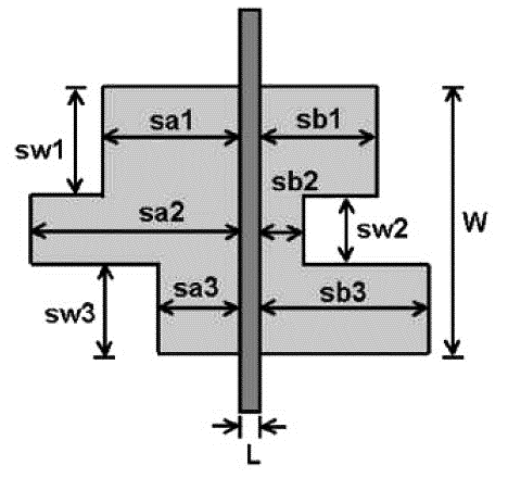
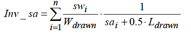
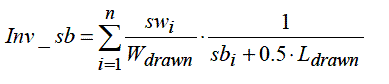
For irregular LOD device like above figure, more instance parameters (swi, sai and sbi) are needed. Then,
Well Proximity Effect Model
Deep buried layers can affect devices located near the mask edge. Some of the ions scattered out of the edge of the photoresist are implanted in the silicon surface near the mask edge, altering the threshold voltage of those devices. BSIM4 considers the influence of well proximity effect on threshold voltage, mobility, and body effect as following:


TMIBSIM4 Model (tmibsim4)
The TSMC Model Interface (TMI) implements a modified version of the BSIM4 model, known as TMIBSIM4. You can activate the tmibsim4 model by specifying the tmiflag and tmipath parameters as follows:
.options tmiflag = 1
.option tmipath = TMI_shared-library_path
Related Topics
Effective Oxide Thickness, Channel Length and Channel Width
Channel Charge and Subthreshold Swing Models
Gate Direct Tunneling Current Model
Return to top