27
EKV MOSFET Model (ekv)
The EPFL-EKV MOSFET model was developed by the Electronics Laboratories, Swiss Federal Institute of Technology (EPFL), Switzerland.
This description concentrates on the intrinsic part of the MOSFET. The extrinsic part of the MOSFET is handled as it is commonly made for other MOSFET models.
The EPFL-EKV MOSFET model is formulated as a single expression, which preserves the continuity of first- and higher-order derivatives with respect to any terminal voltage, in the entire range of validity of the model.
The EPFL-EKV MOSFET model version 2.6 includes modeling of the following physical effects:
- Basic geometrical and process-related aspects, such as oxide thickness, junction depth, and effective channel length and width
- Effects of doping profile and substrate effects
- Modeling of weak, moderate, and strong inversion behavior
- Modeling of mobility effects due to vertical and lateral fields and velocity saturation
- Short-channel effects, such as channel-length modulation (CLM), source and drain charge-sharing (including for narrow channel widths), and reverse short-channel effect (RSCE)
- Quasi-static charge-based dynamic model
- Thermal and flicker noise modeling
- First-order nonquasi-static model for the transadmittances
Coherence of Static and Dynamic Models
All aspects regarding the static, the quasi-static, and nonquasi-static dynamic and noise models are all derived in a coherent way from a single characteristic, the normalized transconductance-to-current ratio. Symmetric normalized forward and reverse currents are used throughout these expressions. The Spectre® circuit simulator supports only one dynamic model, a charge-based model for the node charges and transcapacitances. The dynamic model, including the time constant for the nonquasi-static model, is described in symmetrical terms of the forward and reverse normalized currents. The charge formulation is further used to express the effective mobility dependence of the local field.
Bulk Reference and Symmetry
Voltages are all referred to the local substrate:
VG = VGB Intrinsic gate-to-bulk voltage
VS = VSB Intrinsic source-to-bulk voltage
VD = VDB Intrinsic drain-to-bulk voltage
VS and VD are the intrinsic voltages, which means that the voltage drop over extrinsic resistive elements is supposed to already be accounted for externally. VD is the electrical drain voltage such that VD ≥ VS. Bulk reference allows the model to be handled symmetrically with respect to source and drain, a symmetry that is inherent in common MOS technologies (excluding asymmetric source-drain layouts).
Equivalent Circuit
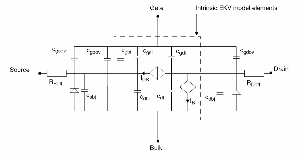
This figure represents the intrinsic and extrinsic elements of the MOS transistor. For quasi-static dynamic operation, only the intrinsic capacitances from the simpler capacitances model are shown in the figure. However, a charge-based transcapacitances model is also available for computer simulation.
Related Topics
Return to top