Physical Resistor (phy_res)
A physical resistor consists of a two terminal resistor (tied between t1 and t2) and two diodes (tied between t1-t0 and t2-t0). The diodes are junction diodes. Under normal operation, the two diodes are reverse biased, but the parameter subtype can reverse the direction of the diodes. If you do not specify t0, ground is assumed. The instance parameters always override model parameters. If you do not specify the instance resistance value, it is calculated from the model parameters.
This device is supported within altergroups.
If R(inst) is not given and R(model) is given,
R(inst) = Rsh * (L - 2 * etchl) / (W - 2 * etch).
If the polynomial coefficients vector (coeffs=[c1 c2 ...]) is specified, the resistor is nonlinear. When nonlinform is set to g, the conductance is
= (1 + c1 * V + c2 * V^2 + ...) / R(inst)
Here V is the controlling voltage across the resistor. It is also the controlling voltage when the model parameter polyarg is set to diff. In this form, the physical resistor is symmetric with respect to V(t1) and V(t2). The branch current as a function of the applied voltage is given by
I(V) = (V / R(inst)) * (1 + 1/2 * c1 * V + 1/3 * c2 * V^2 + ...)
where ck is the kth entry in the coefficient vector.
If the model parameter polyarg is set to sum, then the controlling voltage is defined as
Vsum = ( (V(t1) - V(t0)) + (V(t2) - V(t0)) )/2
Here, Vsum is the controlling voltage between the resistor and the substrate, t0. In this case, the device becomes asymmetric with respect to V(t1) and V(t2). The branch current as a function of the applied voltage for this case is given by
I(Vsum) = (V / R(inst)) * (1 + c1 * Vsum + c2 * Vsum^2 + ...)
The large-signal conductance is given by
G(Vsum) = I/V = (1 + c1 * Vsum + c2 * Vsum^2 + ...) / R(inst)
Note, since the device is asymmetrical, the small-signal model is more complicated then a simple conductance.
When nonlinform is set to r, the resistance is
= R(inst) * (1 + c1 * V + c2 * V^2 + ...).
The resistance as a function of temperature is given by:
R(T) = R(tnom) * [1 + tc1 * (T - tnom) + tc2 * (T - tnom)^2].
If you do not specify the junction leakage current (is) and js is specified, the leakage current is calculated from js and the device dimensions.
is = js * 0.5 * (L - 2 * etchl) * (W - 2 * etch)
If you specify the instance capacitance or the linear model capacitance, linear capacitors are used between t1-t0 and t2-t0. Otherwise, nonlinear junction capacitors are used and the zero-bias capacitance values are calculated from the model parameters.
If C(inst) is not given and C(model) is given,
C(inst) = 0.5 * Cj * (L - 2 * etchlc) * (W - 2 * etchc) + Cjsw * (W + L - 2 * etchc - 2 * etchlc).
If the capacitance is nonlinear, the temperature model for the junction capacitance is used. Otherwise, the following equation is used.
C(T) = C(tnom) * [1 + tc1c * (T - tnom) + tc2c * (T - tnom)^2].
Thermal Noise

R is the resistor value and T is the temperature.
Shot Noise for the Junctions
Where I is the current flow through the junction.
Flicker Noise for the Resistor
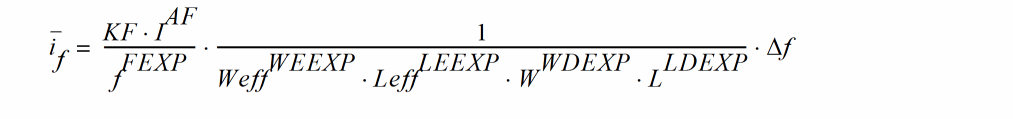
Where KF, AF, FEXP, WEEXP, LEEXP, WDEXP and LDEXP are model parameters, I is the current, W and L are the device width and length, Weff=W-2ETCH and Leff=L-2ETCHL.
Flicker Noise for the Junctions
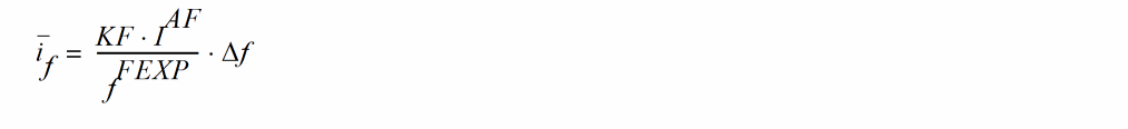
Where KF, AF and FEXP are model parameters, I is the current, and f is the frequency.
Sample Instance Statement
res1 (net9 vcc) resphy l=1e-3 w=2e-6
Sample Model Statement
model resphy phy_res rsh=85 tc1=1.53e-3 tc2=4.67e-7 etch=0 cj=1.33e-3 cjsw=3.15e-10 tc1c=9.26e-4
Instance Syntax
Name 1 2 [0] ModelName parameter=value ...
Instance Parameters
|
Estimated operating region. Spectre generates output number (0-1) in a rawfile. Possible values are |
|
|
Should resistor generate noise. Possible values are |
|
The w and l parameters are scaled by the option parameters scale and scalem. The values of w and l printed by Spectre are those given in the input file. These values may not have the correct units if the scaling factors are not unity. The correct effective resistor dimensions are stored in the output parameters. You can obtain these dimensions with the info statement. You can delete the diodes from the device by either setting is=0 or subtype=poly. You can also set both mj and mjsw to zero to make the capacitance linear but still calculated from the device geometry. If subtype=poly, the linear capacitors will always be used irrespective of the values of mj and mjsw.
Model Syntax
model modelName phy_res parameter=value ...
Model Parameters
Substrate type parameters
Resistance parameters
|
Vector of polynomial conductance or resistance coefficients. |
|
|
The form of the nonlinear resistance. Possible values are |
|
|
Polynomial model argument type. Possible values are |
Temperature effects parameters
Junction diode model parameters
Junction capacitance model parameters
Device size parameters
Noise model parameters
DC-mismatch model parameters
Output Parameters
Operating-Point Parameters
|
Estimated operating region. Spectre generates output number (0-1) in a rawfile. Possible values are |
|
Related Topics
Two Terminal Resistor (resistor)
Return to top