R2 Model (r2)
The R2 model is a nonlinear 2-terminal resistor model. The model does not include parasitic capacitances. As an option, the model can include self-heating. The nonlinearity form is from Agere Systems, and effectively implements first and second order electric field coefficients of resistance. The R2 model does not have the numerical problems that can arise in polynomial models. Although empirical, the form of the nonlinearity can model data reasonably well, especially for velocity saturation effects which are important in short resistors.
Usage
r<instanceName> (<node1> <node2> [dt]) <modelName> <instanceParameters> model <modelName> r2 <modelParameters>
r<name> (<node1> <node2> [dt]) r2 r=<resistanceValue> [tc1=<tc1Value>] [tc2=<tc2Value>]
The dt node is the rise above the local temperature caused by the thermal power dissipated by the device being modeled.
r137 (n1 n2) rnpoly1 w=1u l=10u
model rnpoly1 r2
+ rsh=100.0 xl=0.2u xw=-0.05u
+ p3=0.12 q3=1.63 p2=0.014 q2=3.79
Equivalent Circuit
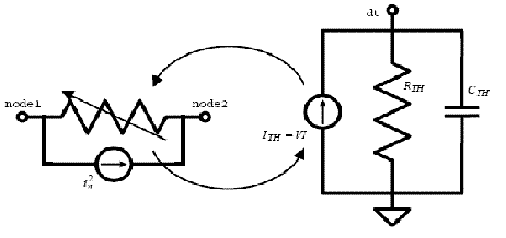
Figure -1 Model Equivalent Network (the thermal sub-network is optional)
Bias Dependence
If V is the voltage between the terminals node1 and node2, then the current flowing from node1 to node2 is
the DC bias dependent resistance is
where R0(T) is the zero-bias resistance at the device temperature (which includes self-heating for the electrothermal version of the model), and the bias-dependent resistance factor is
The electric field E can be calculated based on either the design length or the effective electrical length, depending on the switch parameter sw_efgeo. This is because, depending upon how the model is used and the model parameters are characterized, there can be effects in the value of xl (the parameter that defines the difference between the design length and the effective electrical length) that are not related to velocity saturation (e.g. if end spreading and/or contact resistance are included in xl). If sw_efgeo is 1 (true), the electric field is calculated from the effective geometry.
otherwise it is calculated from the design geometry,
In both cases, an additional length offset dxle is included to allow flexibility and optimization in fitting data by separating the lengths used for resistance and field nonlinearity calculation. Although there is a singularity at V = E = 0 because of the absolute value operation in Equation 2-3, the derivative of Equation 2-1 with respect to voltage is defined and continuous up to third order. The fourth order derivative does not exist at V = 0 and its left limit does not equal its right limit there.
For the electrothermal version of the model, the thermal power is calculated as
and the powers that flow through the thermal resistance and thermal capacitance are
respectively, where T(dt) is the local temperature rise due to self-heating and the thermal conductance and capacitance are gTH and cTH, respectively. The thermal admittance is
yTH = gTH + jωcTH.
The thermal power after simulation convergence is:
Geometry Dependence
The basic calculation for the (zero bias) resistance of a resistor is R0 = rshL/W. Because of several physical effects, the length and width used in this calculation differ from the design (or mask) length and width that define the resistor layout.
The r2 model incorporates a simple, fixed offset between design and effective (electrical) length and width. Because subcircuit models for resistors can consist of multiple resistance sections connected in series, it is desirable to be able to switch on and off the end corrections for length to facilitate implementation of such multi-section models. This is the function of the c1 and c2 instance parameters of the r2 model. The effective length offset is
(which is zero if neither end is contacted, xl if both ends are contacted, and xl/2 if only one end is contacted).
The design length and width, in units of microns, are
where conversions from optical shrinking and unit scale conversion are included. If scale is 1 then l and w should be specified on model instances in meters. If scale is 1.0e-6 then l and w should be specified in units if microns. The effective electrical dimensions are
There are three modes of geometric calculation based on the instance parameters w, l, and r. All modes are based on resistance being specified (or calculated), at zero applied bias and at the nominal device temperature specified by the parameter tnom. The order of importance of considering the instance parameters is (in order of from most to least important) width, length, and resistance. If all are specified, the instance r value is ignored, and resistance is calculated from the specified length and width.
and the effective width is calculated
and possibilities of zero resistance or length, and error conditions of negative length or width, are handled.
If resistance is specified, and length is not specified, then
and again possibilities of zero resistance and error conditions of negative length or width are handled.
For any other combination of instance parameter specification (resistance is not specified, or if it is then both width and length, which override resistance specification, are also specified), then the resistance is calculated from the geometry,
and zero resistance or conductance, and negative length or width errors, are handled.
Although end effects, such as spreading resistance and contact resistance, are assumed to be modeled via the xl parameter, the temperature coefficients of the end effects may differ from those of the body of the resistor. Simple analysis shows that these different temperature coefficients can be accounted for by introducing inverse length dependence to the temperature coefficients. A width dependence of temperature coefficients of resistance is also included in the model. Therefore in the R2 model,
where the length dependence is switched on, off, or halved, depending on whether the resistor is contacted at both ends, not contacted, or contacted at only one end, respectively. The dependence of the temperature coefficients on whether a resistor is contacted or not enables consistent modeling of temperature coefficients for single or multiple section models.
The thermal conductance and capacitance include area, perimeter, and fixed components. Asymptotically for a large area device, the heat flow is perpendicular to the plane of heat generation in the resistor, and the heat energy stored in a device depends on its volume, hence the area dependent component. For a long resistor, as it becomes narrower, more of the heat flow is conducted by a fringe path at the edges of the device, hence the perimeter dependent component. As both length and width decrease, the thermal conditions in the device asymptotically approach that of a point source in an infinite medium, hence the fixed component. The thermal conductance and capacitance are therefore
where the area and perimeter are calculated as
The calculated perimeter therefore depends on whether the ends are contacted or not. Often, the design dimensions of the body of a resistor differ from the overall dimensions of the device, for example if the design length is considered to be the unsolicited length of a poly resistor, the total resistor length will typically include silicided contact regions. So it is not readily apparent what dimension should be used in calculation of the thermal conductance and capacitance. That is why the design dimensions, rather than some effective dimensions (whose value is calculated to best fit DC electrical data), are used. This turns out to be fine (with the exception that differences between the perimeter components along length and width dimensions are ignored), because if there is some difference Δ between design and effective dimensions for thermal conductance modeling, then for a device contacted at both ends
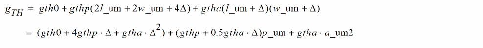
therefore, any difference between design and effective dimensions can be taken into account by appropriate characterization of the fixed, perimeter, and area component parameters.
Because the local thermal conductance differs between the edge of a device and the center of a device, it is higher at the edge because of fringing conductance, the temperature of a resistor undergoing self-heating is not spatially uniform, but is lower at the edges than in the middle. This is not taken into account in the R2 model.
Temperature Dependence
The zero-bias resistance R0 varies with temperature as
where R0,nom is the nominal value of the zero-bias resistance, at the nominal temperature tnom, dT is the temperature difference (including self-heating, if that form of the model is used) with respect to tnom, and
are first (linear) and second (quadratic) order temperature coefficients. These coefficients have both a width dependence and a length dependence, the latter to enable modeling of resistors that have different temperature coefficients for end resistance (which includes contacts and contact enhancement regions) compared to body resistance without having to implement a sectional (subcircuit) model with explicit end and body resistance components. The width and length dependency is detailed in the section on geometry dependence — see Equation 2-20 and Equation 2-21. Smooth limiting of the resistance temperature coefficient in (Equation 2-22) is implemented to limit its lower value to 0.01.
For the isothermal version of the model the temperature difference dT is calculated statically based on the device temperature (which can vary from the circuit ambient temperature by setting the instance parameter trise, which is the local device temperature difference with respect to the circuit ambient temperature). For the electrothermal version of the model dT is calculated dynamically and self-consistently with the power dissipation of the device.
The flicker noise coefficient varies with temperature as
where kfn and tc1kfn are model parameters.
Noise
The noise model comprises two components, a thermal (white) noise component and a flicker ker (1/f ) noise component. These components are noise current spectral density (in A2/Hz ) that are implemented as a noise current sources in parallel with the resistance element.
The thermal noise component is based on the DC conductance of the device,
where k is Boltzmann’s constant, TK is the device temperature (in Kelvin, including the effect of self-heating), G0 is the zero-bias conductance of the resistor (at the temperature T), and rFactor is the bias-dependent (DC) resistance factor (Equation 2-3).
The flicker noise component is DC current dependent (Equation 2-2), and scales with geometry per the physical restrictions noted in Equation 2-3.
where f is frequency (in Hz), afn and bfn are model parameters, KFN(T) is the temperature dependent flicker noise coefficient (Equation 2-28), I is the DC current in the resistor, and W and L are the resistor width and length, respectively, in units of micron. If the switch parameter for flicker noise geometry calculation sw_fngeo is 0 (false) then W and L are design geometries, w_um and l_um respectively, else if it is 1 (true) then W and L are effective geometries, weff_um and leff_um respectively.
Description and Details
The voltage nonlinearity of the device resistance is
where R0 is the zero bias resistance of the resistor, E=V/L is the electric field across the device, p3 and q3 are parameters of the effective first order (linear) electric field coefficient, and p2 and q2 are parameters of the effective second order (quadratic) electric field coefficient. Because the nonlinearity is based on field, rather than voltage, it scales with geometry.
For q3E somewhat greater than 1, the cubic component of the model becomes
therefore this term approximates a linear (first order) field dependence of resistance with a coefficient of value p3.q3.
For q2E somewhat less than 1, the quadratic component of the model becomes
therefore this term approximates a quadratic (second order) field dependence of resistance with a coefficient of value 0.5p2²q22. For high fields this component becomes
and it turns out that the behavior embodied in Equation 2-33 and Equation 2-34 is quite accurate for modeling velocity saturation, which is a significant component of nonlinearity for shorter resistors.
To ensure that the resistance does not become negative,
are enforced. This also precludes the model exhibiting a negative differential resistance (NDR). NDR is observed in some devices, but this is from self-heating effects in resistors with positive temperature coefficients. This behavior should therefore be modeled using the electrothermal version of the model.
In SPICE-like simulators, which are based on modified nodal analysis (MNA), it is preferable to formulate models as voltage controlled current sources (VCCS’s). This is the default for the R2 model. For small resistance values this can cause numerical problems, and the MNA formulation is not possible for zero valued resistors (which have infinite conductance). For small resistance values it is better to switch to a current controlled voltage source (CCVS) formulation. Implicitly, this increases the matrix size for MNA analysis, as the current through the CCVS becomes a system variable. The R2 model includes a parameter rthresh, and if the total (not per segment, but r/m) resistance at zero bias is less than rthresh, the model switches to a CCVS formulation for numerical stability and to be able to work properly for zero valued resistors. This makes the model implicit as the formulation is effectively
V=I·R(V ).
Related Topics
Two Terminal Resistor (resistor)
Component Statements
Instance Syntax
Name 1 2 ModelName parameter=value ...
Name 1 2 r2 parameter=value ...
Instance Parameters
|
Should resistor generate noise. Possible values are |
|
Model Syntax
model modelName r2 parameter=value ...
Model Parameters
Operating-Point Parameters
Related Topics
Two Terminal Resistor (resistor)
Return to top