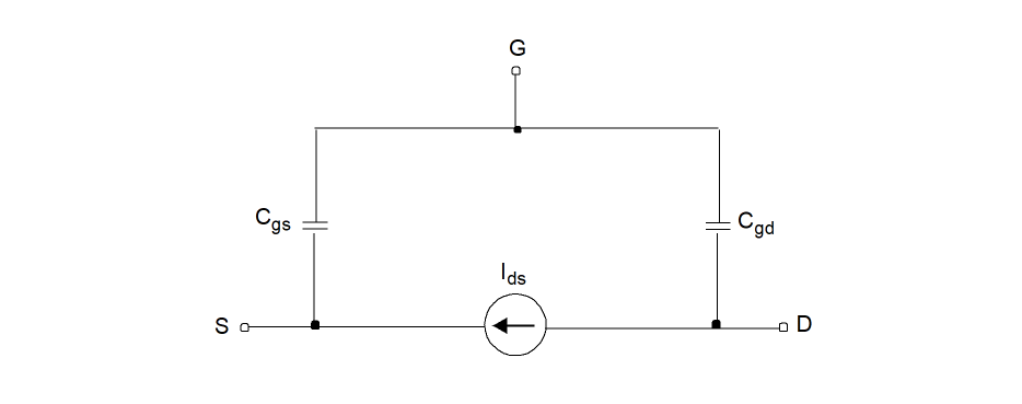
Amorphous-Si TFT Model (ATFT)
Equivalent Circuit
Model Features
Features of the ATFT model include:
-
The unified DC model covers all regimes of operation
-
The model parameters are automatically scaled to accurately model a wide range of device geometries
-
The modified charge control model includes induced charge trapped in localized states
-
Above threshold includes:
-
Field effect mobility becoming a function of gate bias
-
Band mobility dominated by lattice scattering
-
Below threshold includes:
-
Fermi level located in deep localized states
-
Realting position of fermi level, incluing deep DOS, back to the gate bias
-
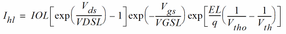
Emperical expression for current at large negative gate biases for hole-induced leakage current
-
Temperature effects include:
-
Linear dependence of threshold voltage
-
Temperature activated field-effect mobility
-
Temperature activated leakage current
-
Dependence of subthreshold slope includinga possible back channel effect.
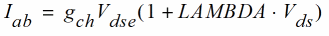
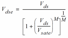
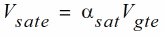
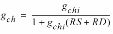
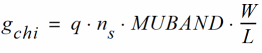
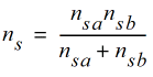
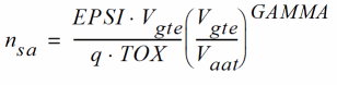
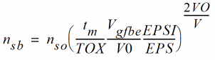
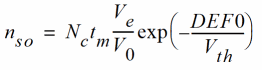
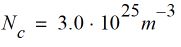
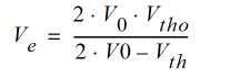
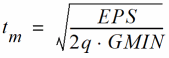
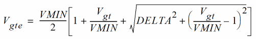
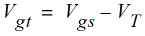
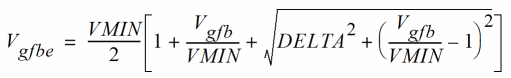
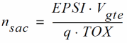
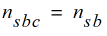
Drain Current
(-107)
(-108)
where
(-109)
(-110)
(-111)
(-112)
(-113)
(-114)
(-115)
(-116)
(-117)
(-118)
(-119)
(-120)
(-121)
(-122)
(-123)
(-124)
(-125)
(-126)
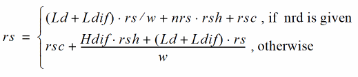
Drain and Source Parasitic Resistance
If ACM is not given,
(-127)
(-128)
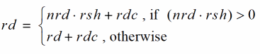
ACM=0:
(-129)
(-130)
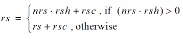
If ACM=1,
(-131)

(-132)

If ACM=2, 3,
(-133)
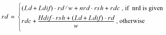
(-134)
Temperature Dependence
(-135)
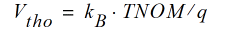
(-136)
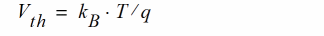
(-137)
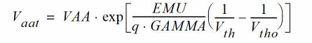
(-138)
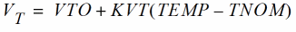
(-139)

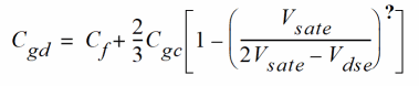
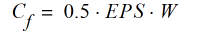
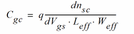
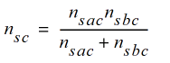
Capacitance
(-140)
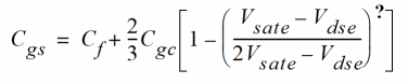
(-141)
(-142)
(-143)
(-144)
(-145)
(-146)
Component Statements
This device is supported within altergroups.
Sample Instance Statement:
m4 (0 2 1 1) nch w=2u l=0.8u
Sample Model Statement
model nch atft type=n
Instance Syntax
Name d g s [b] ModelName parameter=value ...
Instance Parameters
|
w (m)
|
Channel width.
|
|
l (m)
|
Channel length.
|
|
m=1
|
Multiplicity factor (number of MOSFETs in parallel).
|
|
trise=0
|
Temperature rise from ambient.
|
|
region=triode
|
Estimated operating region. Possible values are off, triode, sat, or subth.
|
|
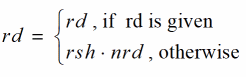
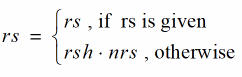
nrd (m/m)
|
Drain squares.
|
|
nrs (m/m)
|
Source squares.
|
|
isnoisy=yes
|
Should device generate noise.
Possible values are yes and no.
|
Model Syntax
model modelName atft parameter=value ...
Model Parameters
Device type parameters
|
type=n
|
Transistor type. Possible values are n or p.
|
Drain current model parameters
|
compatible=spectre
|
|
|
Spice compatible flag. Possible values are spectre, spice2, spice3, cdsspice, spiceplus, eldo, or sspice.
|
|
cdnver=1
|
Cadence version selector.
|
|
vto=0 V
|
Zero-bias threshold voltage.
|
|
lambda=0.0008 1/V
|
Channel length modulation parameter.
|
|
tox=1e-7 m
|
Thin-oxide thickness.
|
|
def0=0.6 eV
|
Dark Fermi level position.
|
|
alphasat=0.6
|
Saturation modulation parameter.
|
|
delta=5
|
Transition width parameter.
|
|
el=0.35 eV
|
Activation energy of the hole leakage current.
|
|
emu=0.06 eV
|
Field effect mobility activation energy.
|
|
eps=11
|
Relative dielectric constant of substrate.
|
|
epsi=7.4
|
Relative dielectric constant of gate insulator.
|
|
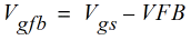
vfb=-3 V
|
Flat band voltage.
|
|
gamma=0.4
|
Power law mobility parameter.
|
|
gmin=1.0e23 1/m3 eV
|
|
|
Minimum density of deep states.
|
|
iol=3.0e-14 A
|
Zero bias leakage current parameter.
|
|
kasat=0.006 1/C
|
Temperature coefficient of ALPHASAT.
|
|
kvt=-0.036 V/C
|
Threshold voltage temperature coefficient.
|
|
m=2.5
|
Knee shape parameter.
|
|
muband=0.001 m2/V s
|
|
|
Conduction band mobility.
|
|
rs=0 Ω
|
Source resistance.
|
|
rd=0 Ω
|
Drain resistance.
|
|
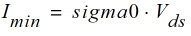
sigma0=1.0e-14 A
|
Minimum leakage current parameter.
|
|
v0=0.12 V
|
Characteristic voltage for deep states.
|
|
vaa=7.5e3 V
|
Characteristic voltage for field effect mobility.
|
|
vdsl=7 V
|
Hole leakage current drain voltage parameter.
|
|
vgsl=7 V
|
Hole leakage current drain voltage parameter.
|
|
vmin=0.3 V
|
Convergence parameter.
|
|
cgdo=0 F/m
|
Gate-drain overlap capacitance.
|
|
cgso=0 F/m
|
Gate-source overlap capacitance.
|
ACM parameters
|
acm=0
|
Area calculation method.
|
|
xw=0.0 m
|
Accounts for masking and etching effects.
|
|
xl=0.0 m
|
Accounts for masking and etching effects.
|
|
ld (m)
|
Lateral diffusion into channel from source and drain diffusion.
|
|
wd=0.0 m
|
Lateral diffusion into channel from bulk along width.
|
|
lmlt=1.0
|
Length diffusion layer shrink reduction factor.
|
|
wmlt=1.0
|
Width diffusion layer shrink reduction factor.
|
|
rsh=0 Ω/sqr
|
Source/drain diffusion sheet resistance.
|
|
rdc=0.0 Ω
|
Additional drain resistance due to contact resistance.
|
|
rsc=0.0 Ω
|
Additional source resistance due to contact resistance.
|
|
ldif=0.0 m
|
Length of heavily doped diffusion adjacent to gate.
|
|
hdif=0.0 m
|
Length of heavily doped diffusion from contact to lightly doped region.
|
|
meto=0.0 m
|
Fringing field factor for gate to source and gate to drain overlap capacitance.
|
|
xj=0.0 m
|
Metallurgical junction depth.
|
Temperature effects parameters
|
tnom (C)
|
Parameter measurement temperature.
|
|
trise=0 C
|
Temperature rise from ambient.
|
Operating region warning control parameters
|
alarm=none
|
Forbidden operating region. Possible values are none, off, triode, sat, subth, or rev.
|
Auto Model Selector parameters
|
wmax=1 m
|
Maximum channel width for which the model is valid.
|
|
wmin=0 m
|
Minimum channel width for which the model is valid.
|
|
lmax=1 m
|
Maximum channel length for which the model is valid.
|
|
lmin=0 m
|
Minimum channel length for which the model is valid.
|
Noise model parameters
|
noisemod=1
|
Noise model selector.
|
|
kf=0
|
Flicker (1/f) noise coefficient.
|
|
af=1
|
Flicker (1/f) noise exponent.
|
|
ef=1
|
Flicker (1/f) noise frequency exponent.
|
|
wnoi=1e-5 m
|
Channel width at which noise parameters were extracted.
|
Operating-Point Parameters
|
type=n
|
Transistor type. Possible values are n or p.
|
|
region=triode
|
Estimated operating region. Possible values are off, triode, sat, or subth.
|
|
reversed
|
Reverse mode indicator. Possible values are no or yes.
|
|
ids (A)
|
Resistive drain-to-source current.
|
|
vgs (V)
|
Gate-source voltage.
|
|
vds (V)
|
Drain-source voltage.
|
|
vth (V)
|
Threshold voltage.
|
|
vdsat (V)
|
Drain-source saturation voltage.
|
|
gm (S)
|
Common-source transconductance.
|
|
gds (S)
|
Common-source output conductance.
|
|
cgd (F)
|
Gate-drain capacitance.
|
|
cgs (F)
|
Gate-source capacitance.
|
|
ron (Ω)
|
On-resistance.
|
|
id (A)
|
Resistive drain current.
|
|
pwr (W)
|
Power at op point.
|
|
i1 (A)
|
Resistive drain current.
|
Return to top