Poly-Si TFT Model (PSITFT)
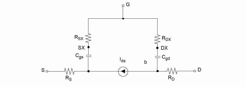
Equivalent Circuit
Model Features
- Unified DC Model includes all four regimes for channel lengths down to 4 um
- AC model accurately reproduces Cgs frequency dispersion
- Automatic scaling of model parameters to accurately model a wide range of device geometries.
- Above threshold
- Sub-threshold
- Leakage Current
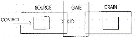
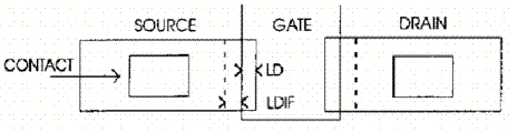
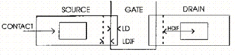
Channel Width and Length
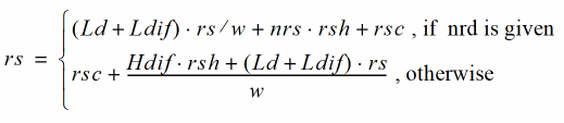
Drain and Source Parasitic Resistance
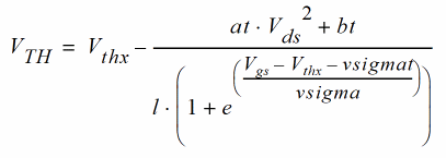
Threshold Voltage
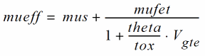
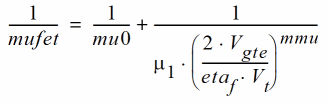
Effective Mobility
Unified Electron Sheet Charge Density Per Unit Area
where
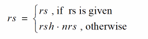
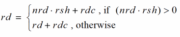
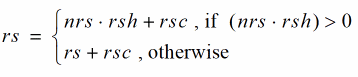
Channel Conductance
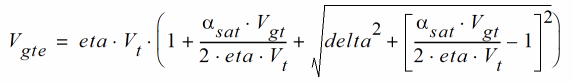
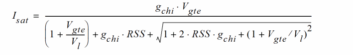
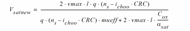
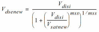
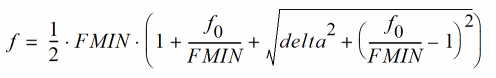
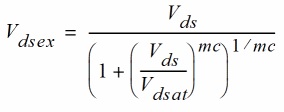
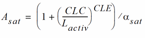
Saturation Voltage
Channel Current
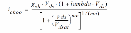
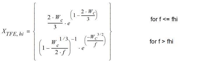
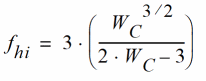
Kink Effect Current
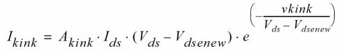
Kink effect current is added to the drain current
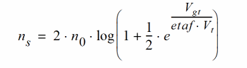
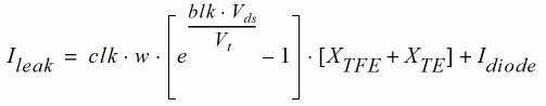
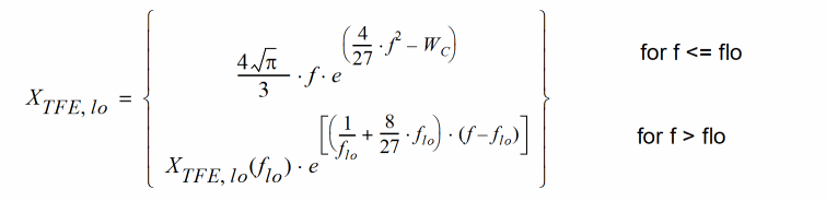
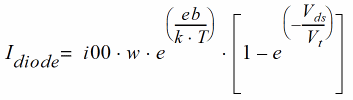
Subthreshold Leakage Current
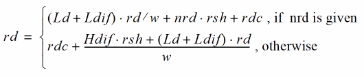
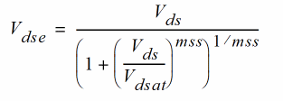
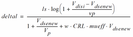
Parasitic Resistance Dependence
If intdsnod=0 , extrinsic characteristics are used.
Else, intrinsic characteristics are used.
Gate-Drain/Source Resistance
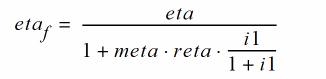
Temperature Dependence
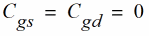
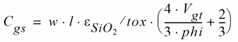
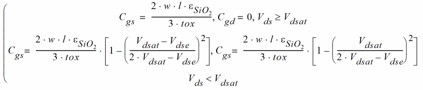
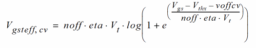
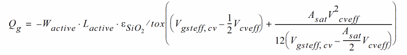
Capacitance
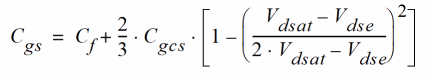
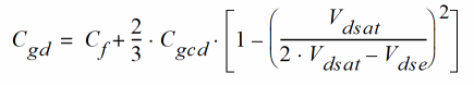
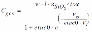
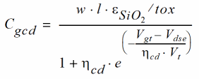
If ZEROC=0,
 if
if  where
where 
 if
if 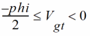
if 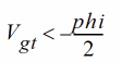
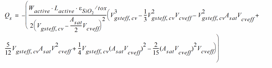
Charge conservation capacitance model
 for Qs evaluation
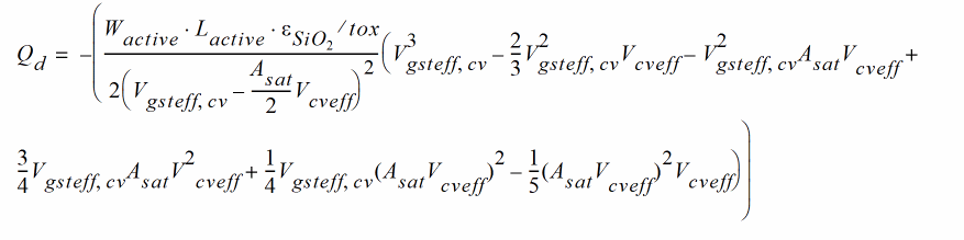
 for Qd evaluation
where
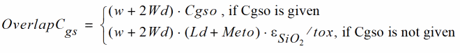
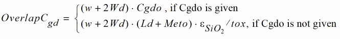
Overlap Capacitances
When capmod=2
For other values of capmod
If Acm parameter is given,
Else,
ACM Option
Scaling Effects
For scaling effects, see Scaling Factors (scale and scalem).
Component Statements
This device is supported within altergroups.
Sample Instance Statement
m4 (0 2 1 1) nch w=2u l=0.8u
Sample Model Statement
model nch psitft type=p
Instance Syntax
Name d g s [b] [t] ModelName parameter=value ...
Instance Parameters
|
Estimated operating region. Possible values are |
|
|
Should resistor generate noise. Possible values are |
|
Model Syntax
model modelName psitft parameter=value ...
Model Parameters
Device type parameters
Drain current model parameters
Temperature effects parameters
Operating region warning control parameters
|
Forbidden operating region. Possible values are |
Default device parameters
Auto Model Selector parameters
Acm related parameters
Capmod=2 related parameters
Special parameters of version 1
Binning parameters
|
Bin parameter unit selector. 1 for microns and 2 for meters. |
|
Output Parameters
Operating-Point Parameters
|
Estimated operating region. Possible values are |
|
Return to top