Model Equations
Effective Channel Length and Width

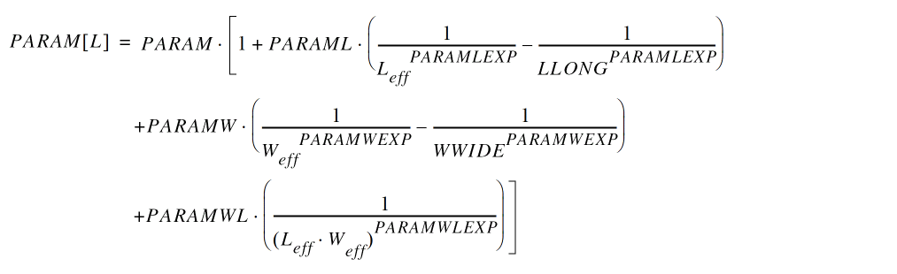
Binning Calculations
For given L and W, each model parameter PARAMi is calculated as a function of PARAM, a length dependent term, LPARAM, width dependent term, WPARAM, and area dependent term PPARAM:

For the list of binnable parameters, refer to the Components Statements section.
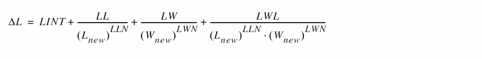
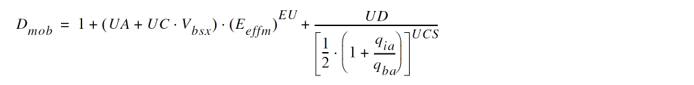
Global Geometrical Scaling
Following scaling formulation is used in global scaling:
Terminal Voltages

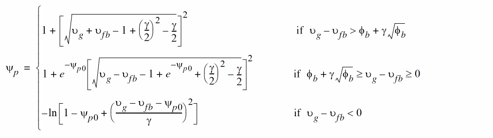
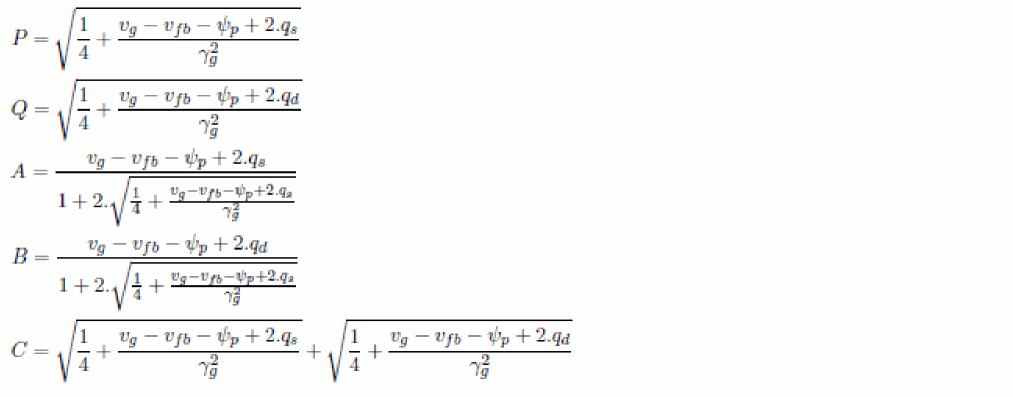
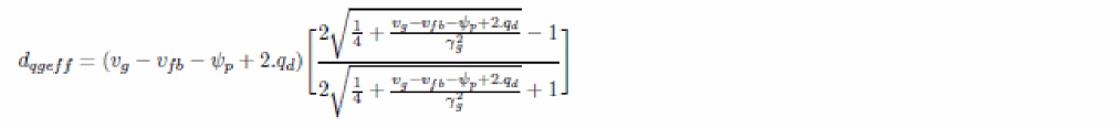
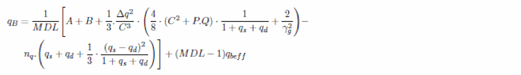
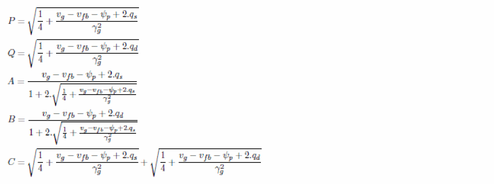
Pinch-Off Potential and Normalized Charge Calculation
Pinch-Off Potential with Poly Depletion
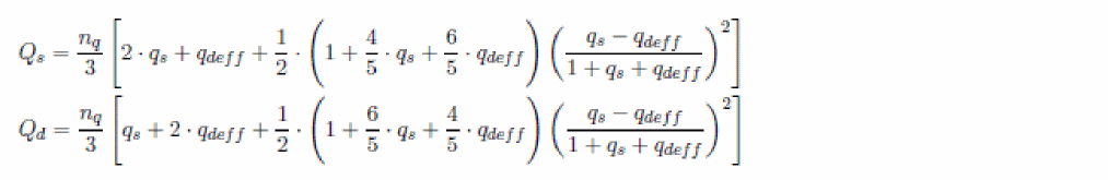
Normalized Charge Density
Inversion charge: Normalized inversion charge density at source/drain is newly derived for BSIM6, and can be obtained as follows:


Short Channel Effects
Vt roll-off, DIBL, and Subthreshold Slope Degradation
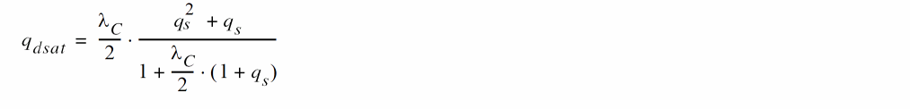
Drain Saturation Voltage
The drain saturation voltage model is calculated after the source-side charge (qs) has been calculated. Vdseff is subsequently used to compute the drain-side charge (qd).
Electric Field Calculations

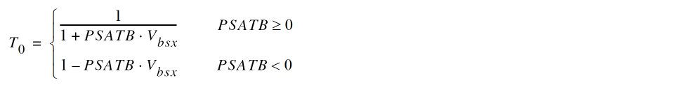
Drain Saturation Voltage (Vdsat) Calculations
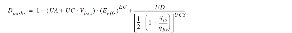


Mobility Degradation with Vertical Field
Parasitic Series Resistance
Bias-Dependent Internal Series Resistance (Rds(V))
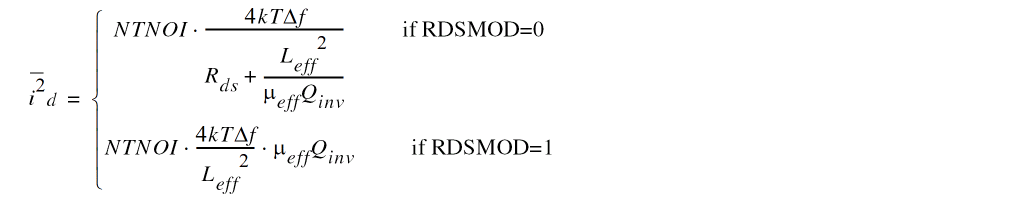
The internal source-drain resistance (Rds(V)) option can be invoked by setting the model selector RDSMOD=0 (internal). Following are the expressions for source/drain series resistance calculation:

Bias-Dependent External Series Resistance (Rs(V) & (Rd(V))
The bias-dependent external resistance model is adopted from BSIM4 and can be invoked by setting model selector RDSMOD=1. BSIM4 and BSIM6 allow the source 36 extension resistance Rs(V) and the drain extension resistance Rd(V) to be external and asymmetric (i.e. here when HVMOD = 1, Rs(V) is connected between nodes S and Si1 and Rd(V) is connected between nodes D and Di1). When HVMOD = 0, Si1 and Si (Di1 and Di) will be shorted. Furthermore, Rs(V) does not have to be equal to Rd(V).
This feature makes accurate RF CMOS simulation possible.
The source/drain series resistance is the sum of a bias-independent component and a bias-dependent component.
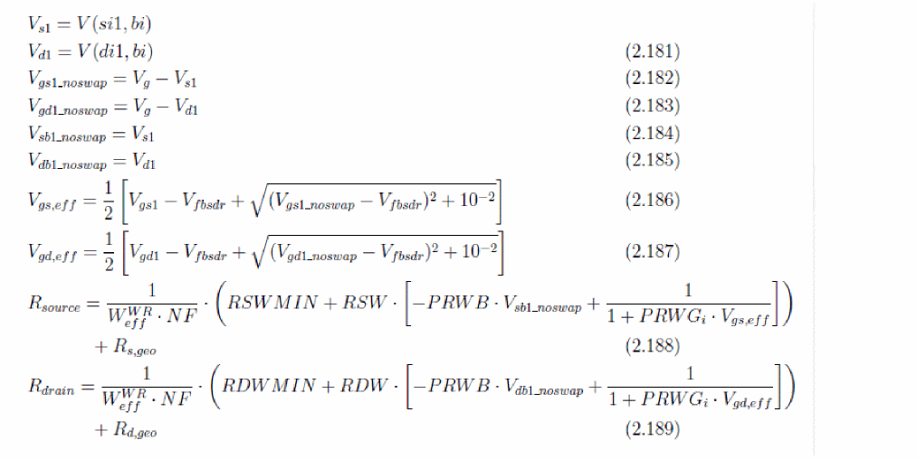
Rs,geo and Rd,geo are the source and drain diffusion resistances.
Sheet Resistance Model

Output Conductance
Channel Length Modulation (CLM)

Drain Induced Barrier Lowering (DIBL)
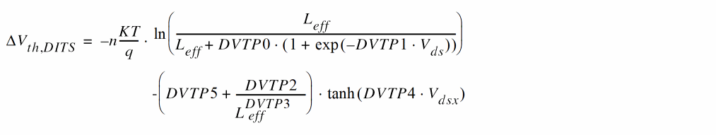
Drain Induced Threshold Shift (DITS)
Substrate Current Induced Body Effect (SCBE)
Velocity Saturation
Current Degradation Due to Velocity Saturation
Effective Mobility
Drain Current Model
Without Velocity Saturation

Including Velocity Saturation

Impact Ionization Model

GIDL/GISL Current Model
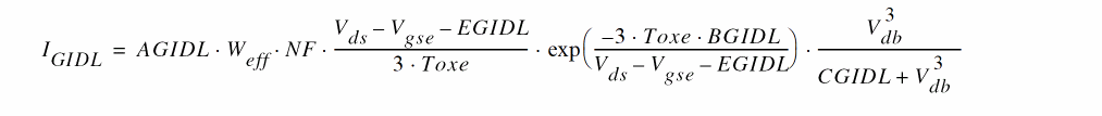
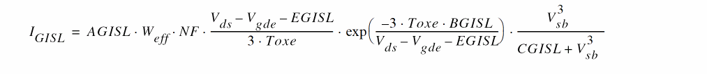
IGIDL/IGISL can be switched off by setting GIDLMOD=0
Gate Tunneling Current Model
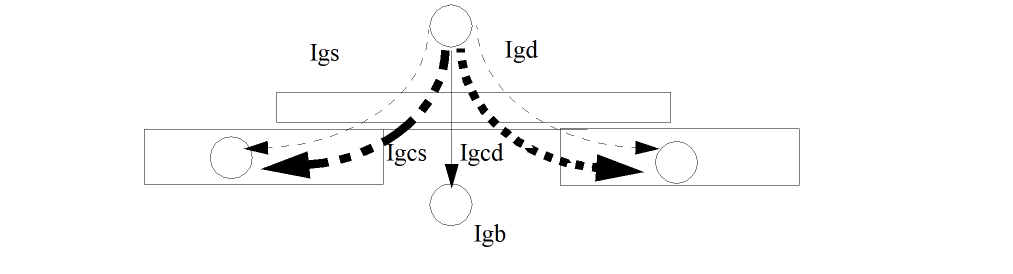
Figure -1 Schematic gate current components flowing between MOSFET terminals
Model Selectors
Two global selectors are provided to turn on or off the tunneling components. IGCMOD=1 turns on Igc, Igs, and Igd; IGBMOD=1 turns on Igb. When the selectors are set to 0, no gate tunneling currents are modeled.
Equations for Tunneling Currents
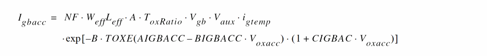
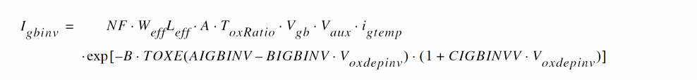
Gate-to-Substrate Current
Gate-to-Channel Current (Igc0) and Gate-to-S/D (Igs and Igd)
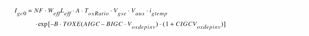
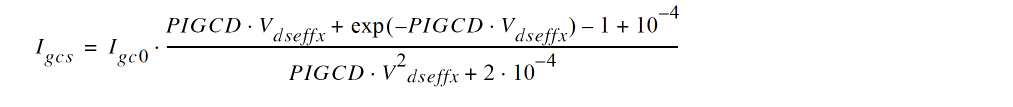
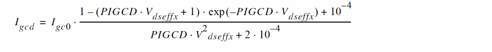
Partition of Igc: Igc=Igcs+Igcd
Igs and Igd
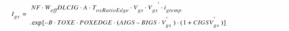
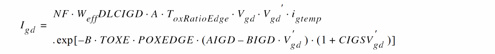
Vfbsd is the flat-band voltage between gate and source/drain diffusions calculated as:
Gate Resistance and Body Resistance Model
Gate Electrode and Intrinsic -Input Resistance (IIR) Model
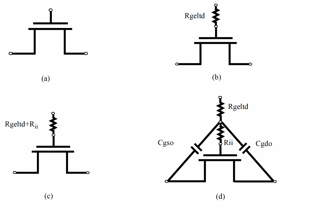
BSIM6 provides four options for modeling gate electrode resistance (bias-dependent) and intrinsic-input resistance (IIR, bias-dependent). The IIR model considers relaxation-time effect due to distributive RC nature of the channel region, and therefore describes the first-order non-quasi static effect. Thus, the IIR model should not be used together with the charge-deficit NQS model at the same time. The model selector RGATEMOD is used to choose different options.
Model Option and Schematic
RGATEMOD=0 (zero resistance). In this case, no gate resistance is generated.
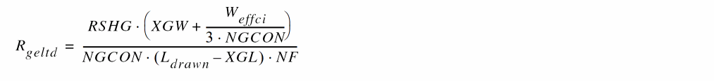
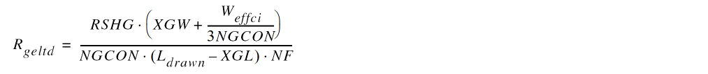
RGATEMOD=1 (constant resistance). Rgeltd is given by the following equation:
RGATEMOD=2 (IIR model with variable resistance):

RGATEMOD=3 (IIR model with two nodes):
Figure -2 Gate resistance network for (a) RGATEMOD=0 (b) RGATEMOD=1 (c) RGATEMOD=2 and (d) RGATEMOD=3
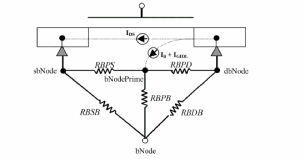
Substrate Resistance Network
Model Selector and Topology
RBODYMOD=2 (On: Scalable Substrate Network)
Figure -3 Topology with the substrate resistance network turned on
Noise Modeling
| Noise Models in BSIM 6.0.0 | Origin |
|---|---|
Flicker Noise Models
FNOIMOD = 1 (Flicker Noise Model): BSIM6’s flicker noise model for FNOIMOD=0 is same as FNOIMOD=1 in BSIM4. The unified physical flicker noise model is smooth over all bias regions.
The physical mechanism for the flicker noise is trapping/detrapping-related charge fluctuation in oxide traps, which results in fluctuations of both mobile carrier numbers and mobilities in the channel. The unified flicker noise model captures this physical process. In the inversion region, the noise density is expressed as [12]
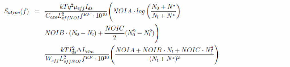
where LeffNOI = Leff - 2 · LINTNOI, µeff is the effective mobility at the given bias condition, and Leff and Weff are the effective channel length and width, respectively.
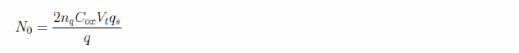
The parameter Nc is the charge density at the source side given by
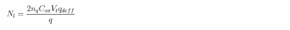
The parameter Nl is the charge density at the drain end given by
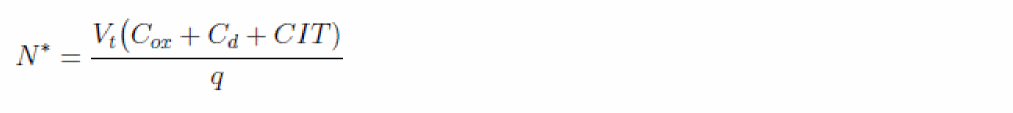
where CIT is a model parameter from DC IV and Cd is the depletion capacitance.
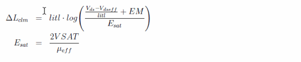
![]() Lclm is the channel length reduction due to channel length modulation and given by
Lclm is the channel length reduction due to channel length modulation and given by
In the subthreshold region, the noise density is written as
The total flicker noise density is

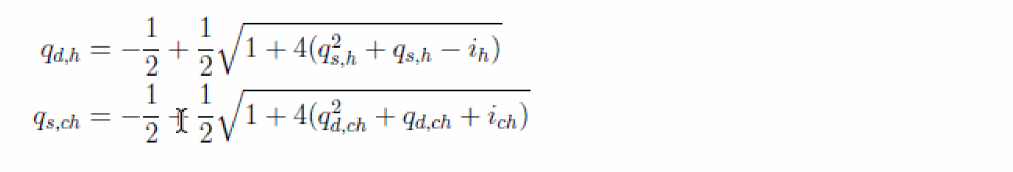
FNOIMOD = 1 (Flicker Noise Model for Halo Transistors): For the noise modeling, it is now assumed that the transistor is composed of two transistors, channel transistor of length L - LH and halo transistor of length LH connected in series and carries same current (IDS) as in single transistor configuration. The individual contribution of the halo and channel transistors to overall noise is obtained using small signal analysis and principle of superposition [13] [14].
Total drain current noise PSD becomes,
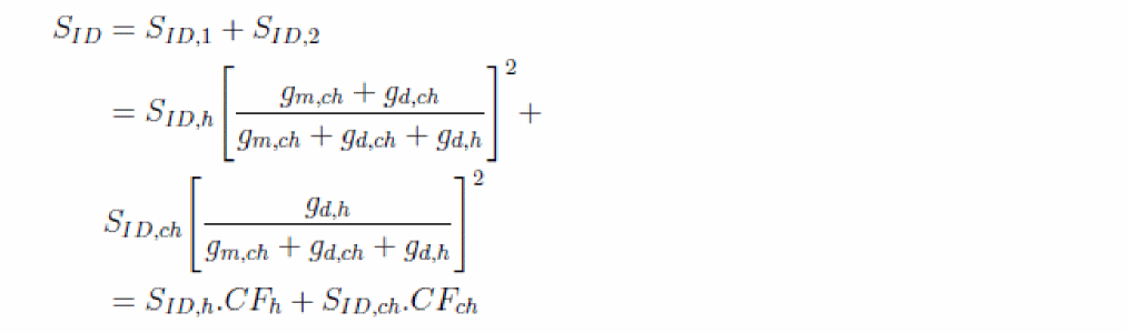
We refer to the multiplying factors to SID,h and SID,ch in (2.320) as contribution factors (CF). Where,
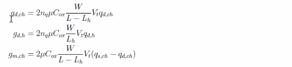
To calculate qd,h and qs,ch, the fact that the same current flows in one transistor and two transistor noise equivalent configuration is used,
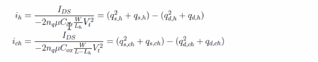
where ih and ich are the normalized drain current of halo and channel transistor respectively. Since IDS is known from DC modeling, the above equations are solved for,
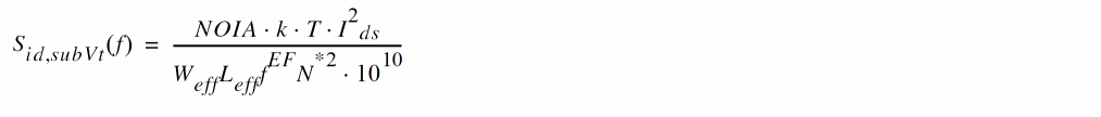
Here we have used the unified model presented in for halo and channel transistors separately, where SID is expressed as
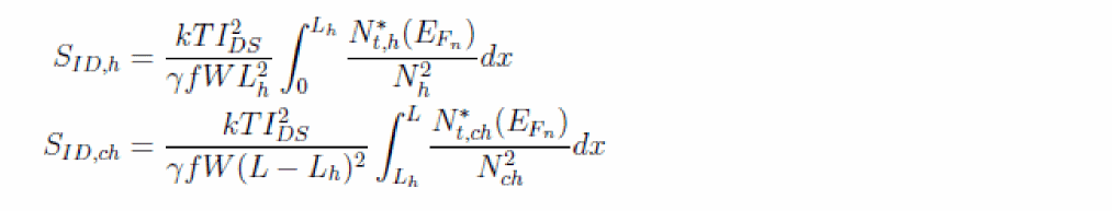
where apparent trap density N*t,ch(h)(EFn) = Ach(h)+Bch(h)Nch(h)+Cch(h)N2ch(h), A, B, C are the noise parameters, ![]() the tunneling parameter, k is the Boltzmann constant and T is the temperature.
the tunneling parameter, k is the Boltzmann constant and T is the temperature.
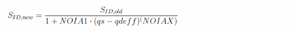
Flicker Noise Tuning Flexibility
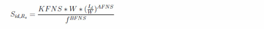
Flicker Noise due to drain and source resistance
Flicker noise due to source resistance (Sid,Rs) is given by
Flicker noise due to drain resistance (Sid,Rd) is given by
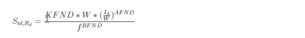
AFNS, BFNS, KFNS, AFND, BFND and KFND are the model parameters.
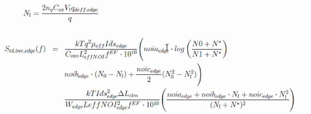
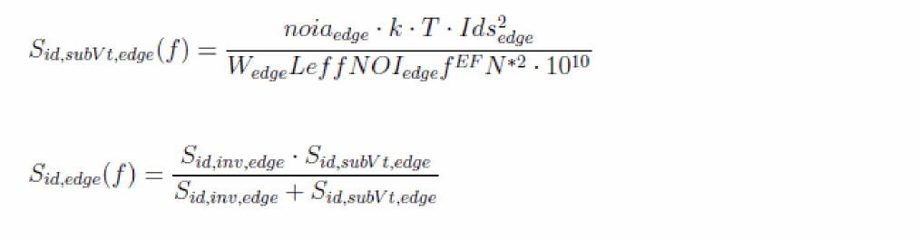
Flicker Noise due to EDGEFET (EDGEFET=1)
The Edge FET Model noise is added to the main flicker noise SID, when the parameter EDGEFET is 1
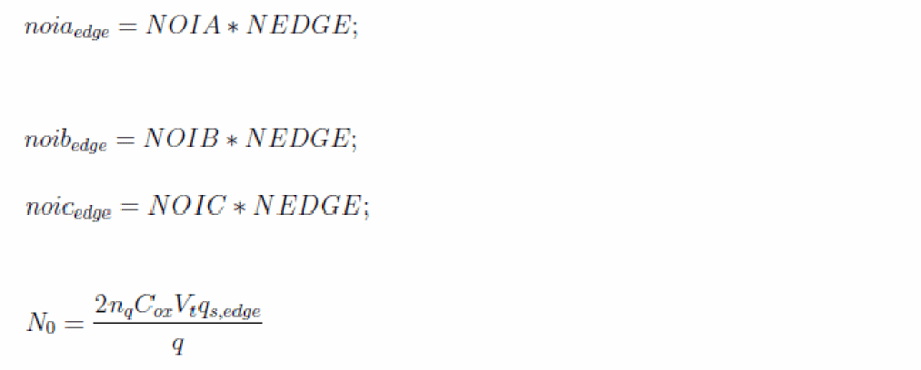
The parameter Nl is the charge density at the drain end given by
Channel Thermal Noise
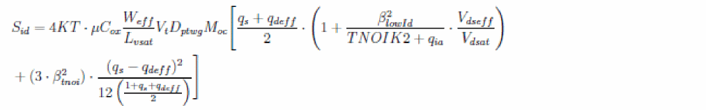
There are two channel thermal noise models in BSIM6. One is a charge-based model (default model) similar to that used in BSIM3v3.2 and BSIM4.7.0 (TNOIMOD=0). The other is the holistic model similar to BSIM4.7.0 (TNOIMOD=2). These two models can be selected through the model selector TNOIMOD.
TNOIDMOD=0 (Charge based model): The noise current is given by:


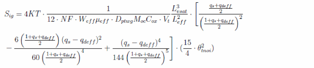

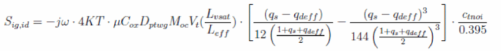

Gate Current Shot Noise
Resistor Noise
The noise associated with each parasitic resistors in BSIM6 are calculated
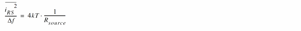
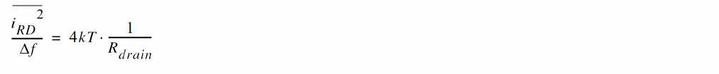


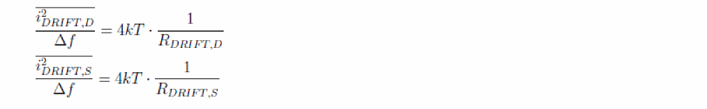
Figure -4 Thermal Network for Self Heating Model
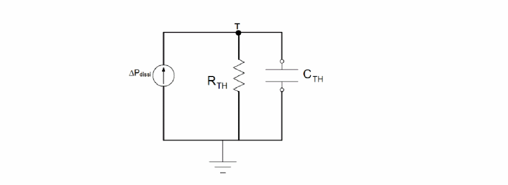
Self Heating Model


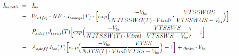
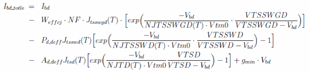
Asymmetric MOS Junction Diode Models
Junction Diode IV Model


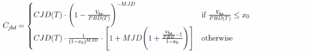
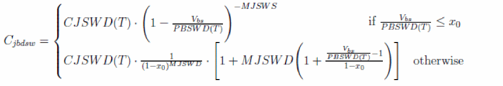
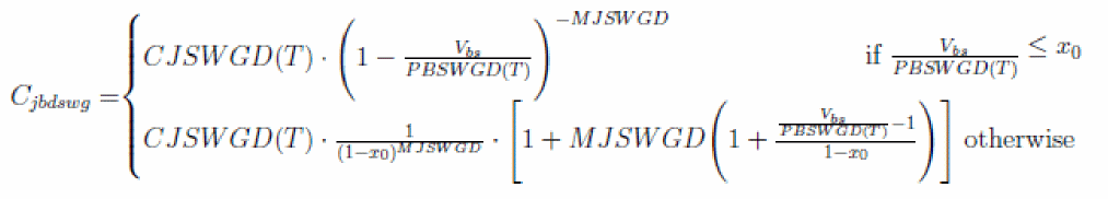
Junction Diode CV Model
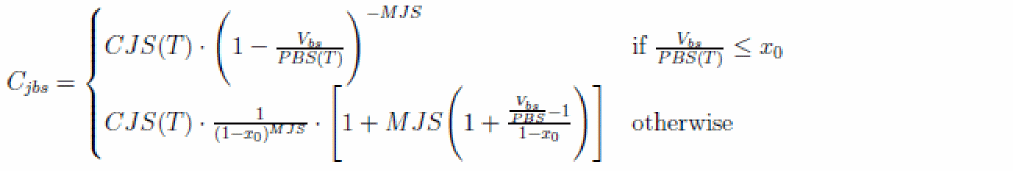
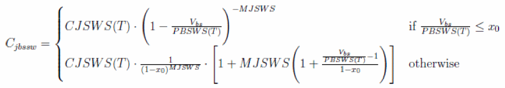
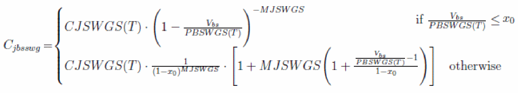
where the value of x0 is taken as 0.9.
where the value of x0 is taken as 0.9.
Layout Dependent Parasitic Models
Effective Junction Perimeter and Area
Pseff computed from NF, DWJ, geoMod, DMCG, DMCI, DMDG, DMCGT, RSH, and MIN.
The effective junction area on the source side is calculated by:
Aseff computed from NF, DWJ, geoMod, DMCG, DMCI, DMDG, DMCGT, RSH, and MIN.
Source/Drain Diffusion Resistance
If (number of sources NRS is given)
Source diffusion resistance Rsdiff is not generated.
Rsdiff computed from NF, DWJ, geoMod, DMCG, DMCI, DMDG, DMCGT, RSH, and MIN.
where the number of source squares NRS is an instance parameter.
Similarly, the drain diffusion resistance is calculated by:
If (number of sources NRD is given)
Drain diffusion resistance Rddiff is not generated.
Rddiff computed from NF, DWJ, geoMod, DMCG, DMCI, DMDG, DMCGT, RSH, and MIN.
Gate Electrode Resistance
Options for Source/Drain Connections
| geomod | End Source | End Drain | Note |
Options for Source Drain Contacts
| rgeomod | End Source contact | End Drain Contact |
Temperature Dependence Models
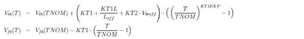
Temperature Dependence of Threshold Voltage
The temperature dependence of Vth is modeled by:

Temperature Dependence of Mobility
Temperature Dependence of Junction Diode IV
Temperature Dependence of Junction Diode CV
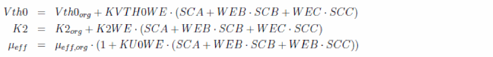
Stress Effect Model Development
Figure -5 Typical Layout of a MOSFET
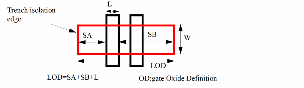
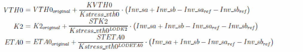
Figure -6 Layout of multiple finger MOSFET
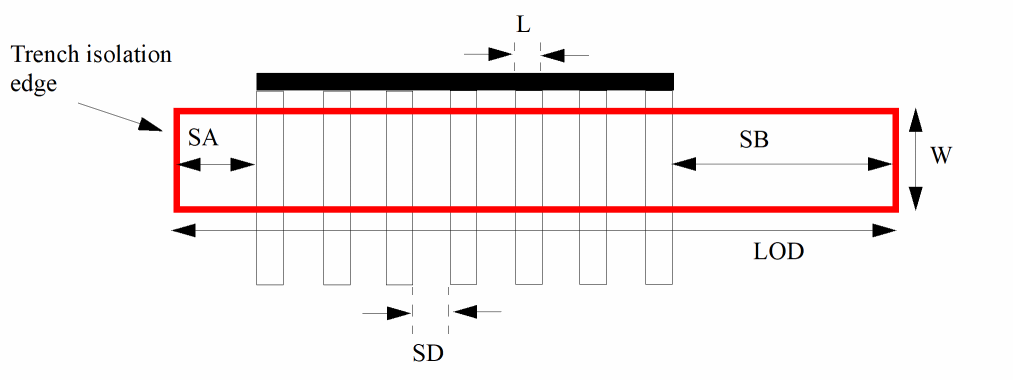
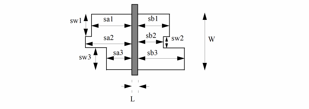
Figure -7 Typical layout of MOS devices with more instance parameters (swi, sai, and sbi) in addition to traditional L and W
Well Proximity Effect Model
C-V Model
Inversion Charge

Bulk Charge

Bulk Charge with poly depletion effect, CLM and velocity saturation effects:

Source and Drain Charges
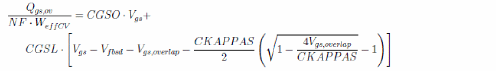
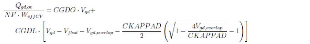
Bias Dependent Overlap Capacitance Model
Outer Fringing Capacitance
Related Topics
Version Update and Enhancements
Component Statements for BSIM6
Return to top