E
Verilog Value Change Dump Stimuli
This chapter introduces the Verilog® value change dump (VCD) and extended VCD (EVCD) file formats, as used in the Spectre® circuit simulator, and provides illustrations to explain the signal information file.
The VCD file (ASCII format) contains information about value changes for selected variables in the circuit design. Spectre supports two types of VCD files:
-
Four-state – represents variable changes in
0,1,x(unknown or “not needed”) andz(tri-state) without providing strength information and port direction -
Extended – represents variable changes in all states and provides strength information and port direction
For more information about EVCD file format, refer to “Enhanced VCD Commands”.
Processing the Value Change Dump File
To process VCD or EVCD files in Spectre, the following statements need to be specified in the netlist file:
vcd_include“vcd_filename”“signal_info_filename”[autostop=yes|no] [insensitive=yes|no]
.vcd “vcd_filename” “signal_info_filename” [autostop=yes|no]
[insensitive=yes|no]
evcd_include “evcd_filename”“signal_info_filename”[autostop=yes|no] [insensitive=yes|no]
.evcd “evcd_filename” “signal_info_filename” [autostop=yes|no]
[insensitive=yes|no]
Spectre replaces the end time in the .tran or tran statement with the time specified in the .vcd/.evcd file when autostop=yes (default is no). If no is specified, the simulation time specified in the .tran or tran statement remains unchanged. For more information on autostop, refer to the Transient Analysis (tran) section in the Spectre Circuit Simulator Reference manual.
Each vcd or evcd statement can only specify one VCD or EVCD file. If a netlist file needs to include multiple VCD or EVCD files, multiple vcd or evcd statements must be used. For example, if a netlist file contains three VCD files, it needs three vcd statements (use the same netlist file format for EVCD files).
Statement 1: vcd_include “file1.vcd” “file1.signal”
Statement 2: vcd_include “file2.vcd” “file2.signal”
Statement 3: vcd_include “file3.vcd” “file3.signal”
Statement 1: .vcd “file1.vcd” “file1.signal”
Statement 2: .vcd “file2.vcd” “file2.signal”
Statement 3: .vcd “file3.vcd” “file3.signal”
VCD and EVCD formats are widely used in digital circuit design and contain different kinds of information for transistor level simulation. You need to provide signal information, such as timing characteristics, voltage threshold, and driving ability of input signals for each VCD or EVCD file. Since VCD and EVCD formats are compatible, Spectre can share the same signal information file.
By default, Spectre handles the VCD and EVCD file content as case insensitive (insensitive=yes). Case sensitivity can be set using the insensitive=no option.
VCD Commands
VCD File Format
The continuous line symbol is the back slash (\) sign and is rarely used in the VCD file. The beginning of a card is indicated by the $command keyword (for example, .$var), and ends with the $end keyword. If an identifier is longer than 1024 characters, and does not fit into a single line, the \ sign must be used to continue the line.
$comment
$commentcomments $end
Description
Comments need to be enclosed within the $comment and $end commands.
Example
$comment
This is a test line.
Definition Commands
In the definition section, the VCD command keywords used to indicate the start of a card begin with a dollar ($) sign. VCD definition commands include: $comment, $date, $enddefinitions, $scope, $timescale, $upscope, $var, and $version. The end of a card is marked with an $end keyword. Multiple lines can be placed between the $command and $end commands.
Spectre supports the following VCD definition section commands:
$date
$datedate$end
Description
The $date command is used to specify the date of the VCD file created. Spectre accepts this command card, but does not process it.
Example
$dateMay 7, 2001$end
$enddefinitions
$enddefinitions$end
Description
The $enddefinitions command indicates where the definition section of the VCD file ends. This command card tells Spectre to treat the rest of the VCD file as the data section. If this command card is missing, Spectre parses the data section incorrectly and issues an error message.
Example
$enddefinitions$end
$scope
$scope[scope_type] [scope_name]$end
Description
The $scope command card switches from the current circuit level to a lower circuit level in the design hierarchy.
Example
$scope module module1 $end
-
Spectre ignores
scope_type, but the command must still be specified to maintain consistency with standard VCD format. -
A matching
$upscopecard must be specified in the VCD file definition section to switch the scope back to the current scope.
$timescale
$timescale[number] [time_unit_prefix]$end
Description
The $timescale command is used to specify the time scale. This time scale applies to all time values in the VCD file, and to its signal information file. The default time is 1 ns.
Arguments
|
The unit prefix. The following unit prefix symbols can be applied to any numerical quantities: |
Example
$timescale 1 ns $end
$timescale 1ns $end
produces the same result, telling Spectre to set the time scale to 1 ns.
$upscope
$upscope$end
Description
The $upscope command card switches from the current circuit level to an upper circuit level in the design hierarchy.
Example
$upscope $end
$var
$var[var_type] [size] [identifier] [reference]$end
$var[var_type] [size] [identifier] [reference] [index_range]$end
Description
The $var command defines the bus to be dumped into the data section.
Arguments
|
The identifier used in the data section; it can be |
|
index_range of [size-1:0].The name of the bit is a combination of the reference and the index.
Examples
$var reg 4 % regA [0:3] $end
the names of the four bits in bus regA are regA[0], regA[1], regA[2], and regA[3]. The netlist file referencing these VCD sources must match these names.
$var reg 1 & b [0] $end
the name of the bit is b[0]. The card defined a bit, not a bus, as a size of 1.
$var reg 1 & c $end
$var reg 4 % regA $end
the names of the four bits in bus regA are regA[3], regA[2], regA[1], and regA[0]. The netlist file referencing these VCD sources must match the names.
$version
$version version $end
Description
The $version command is used to specify the version of the VCD file created. Spectre accepts this command card, but does not process it.
Example
$version spectre B2001.2.10 $end
Data Commands
In the VCD data section, a time point that starts with a number (#) sign (for example, #100) indicates the beginning of a new card. This card continues until it reads the line before the next card (cards can have multiple lines). It can also contain data values and a command block. A command block begins with one of the following command keywords, $comment or $time_value, and ends with $end.
data
Description
Data is divided into two types that each have their own format:
The bus data is for buses defined by $var, with a size greater than one. The bit data applies to the bus defined by $var, with a size equal to one. The bus data format is Bvalue bus_identifier whereas the bit data format is value bus_identifier.
Examples
b0101 %
the bus with identifier % (defined by $var) has a binary value of 0101.
1&
the one bit bus with identifier & (defined by $var) has a binary value of 1.
The valid characters for specifying the value are: 0, 1, x, X, z, and Z. Of these characters, x and X are treated as 0 for the input signal, and do not need a vector check for the output signal. The z and Z characters are treated as floating to high-impedance for the input signal, and do not need a vector check for the output signal.
time_value
#time_value
Description
Each time value (point) is the beginning of a card in the data section.
Example
Time value is equal to 100 time units (time unit is defined by $timescale).
Signal Information File
The signal directions are specified in the signal information file. To input signals, Spectre applies stimuli to the simulation. The values of the output signals are used to perform a vector check against the simulation results, and vector errors are generated if mismatches occur. The enable signals are required to control the bi-directional signal behavior as input or output signals. All other signals in the VCD or EVCD file, not specified in the signal information file, are ignored by the simulator (warning messages are issued for these signals, based on the scopes specified in the signal information file).
The time scale of the time related cards in the signal information file are controlled by the $timescale card in the VCD file. For example, if $timescale is set to 1 ns and .tdelay to 2, a delay of (2 * 1ns) occurs.
The signal name in the signal information file can be specified by using the bus name or a wildcard. The signal name specified in the VCD file is in bus/bit format. Table E-1 provides examples.
| VCD File | Signal Information File |
|---|---|
The example in Table E-2 shows an incorrect naming format.
| VCD File | Signal Information File |
|---|---|
.hier statement can be used to switch to hierarchical name mapping to precisely match signals).Signal Information File Format
A comment line begins with asterisk (*) or dollar ($) signs.
A continuous line is indicated by a plus (+) sign.
The maximum length of a line is 1024 characters. If a card is longer than 1024 characters, you need to use the continuous line for the card.
To process VCD and EVCD formats, the following signal characteristics need to be defined in the signal information file:
Signal Matches
In this section, the following statements define the signal matches between the VCD and analog netlist files, signal directions, and output vector check.
.alias
.aliastarget_busname alias_name
Description
The .alias statement is used to modify the name of the signal bus in the VCD/EVCD file to match the signal name in the netlist file.
By default, Spectre maps the bus delimiter from "*[*]" in VCD file to "*<*>" in the analog netlist. For example, the default setting is as follows:
You can use the following alias statement to alias the VCD signal top.hier1.hier2.*[*] to SPICE top level *<*>:
.alias top.hier1.hier2.*[*] *<*>
.alias statement in hierarchical signal name mapping, refer to “Hierarchical Signal Name Mapping”.Examples
.alias *[*] *[*]
tells Spectre to keep square brackets as the bus limiter in an analog netlist. This .alias statement is required because *[*] is mapped to *<*> by default (see Table E-3).
| Bus Name | Signal Name |
|---|---|
.alias sig_*[*] vec_*<*>
tells the simulator to change the square brackets to angular brackets (see Table E-4).
| Bus Name | Signal Name |
|---|---|
.alias sig_* vec_*
tells the simulator to change the prefix of the signal names from sig_ to vec_ (see Table E-5).
| Bus Name | Signal Name |
|---|---|
.scope
.scopescope_name1 [scope_name2 ... scope_nameN]
Description
The .scope statement specifies the target scope located in the definition section of the VCD file. Only the signals defined in the specified scope are processed. Multiple .scope statements in a signal information file are supported.
Arguments
|
The name of the scope specified in the VCD file by the |
Example
.scope module1 module2
tells Spectre to process the signal located in scope module1 and module2.
.in
.insignal_name1 signal_name2 ... signal_nameN
Description
The .in statement defines the specified bus as the input bus.
Arguments
Example
$var reg 4 % b [0:3] $end
$var reg 1 * a $end
$var reg 1 & c [4] $end
$var reg 4 % d [0:3] $end
.in b[0:3] a c[4] d[*]
Defines b[0:3], a, c[4], and d[0:3] as the input signals.
.out
.out signal_name1 signal_name2 ... signal_nameN
Description
The .out statement defines the specified bus as the output bus.
Arguments
Example
$var reg 4 % b [0:3] $end
$var reg 1 * a $end
$var reg 1 & c [4] $end
$var reg 4 % d [0:3] $end
In the signal information file
.out b[0:3] a c[4] d[*]
Defines b[0:3], a, c[4], and d[0:3] as the output signal.
.bi
.bi‘enable_signal_expr’signal_name1signal_name2...signal_nameN
Description
The .bi statement defines the specified bus as the bidirectional bus.
The enable signal can be from a VCD/EVCD or an analog netlist file. When an enable signal is from an analog netlist file, it can also be defined as an output signal for a vector check or only used as an enable signal. If a VCD signal is used as an enable signal, it must be declared an input using the .in statement and located in the VCD file. Different from enable statements in the vector file, the logic voltage threshold of an analog enable signal is defined by the .voh and .vol statements.
The .alias statement can be used to perform name mapping for the enable signal. In hierarchical signal name mapping (.hier 1), a hierarchical structure for the analog netlist file is supported for the enable signal. A period (.) can be used as the hierarchical delimiter to specify the hierarchical signal, and the hierarchical delimiter can be mapped to other delimiters by the .alias statement.
Bit-wise logic operators are supported in an enable signal expression: & (AND), | (OR), ^ (XOR), and ~ (NOT). Additional operators can be created using a combination of the supported operators. The order of processing for the logic operators is NOT > AND > OR, XOR (OR and XOR are processed at the same time). You can use parentheses () around the operators to change the processing order.
Arguments
|
The expression for the enable signals. The bidirectional bus switches to output mode only when its value is high. |
|
Examples
$var reg 4 % b [0:3] $end
$var reg 1 & en $end
.bi en b[0:3]
defines b[0:3] as the bidirectional signal, which is controlled by the en signal. When en is high, b[0:3] becomes the output signal.
$var reg 4 * myBi [0:3] $end
$var reg 1 # en $end
bi ~en myBi[0:3]
defines myBi[0:3] as the bidirectional signal, which is controlled by the en signal. The enable signal is appended with a tilde (~) sign, so unlike the first example, the en is now high, myBi[0:3] becomes the input signal, and vice versa.
$var reg 4 * myBi_1 [0:3] $end
$var reg 1 # en $end
.hier 1
.bi ‘en & (ana_en1 ^ X1.ana_en2)’ myBi_1[0:3]
.voh 1.5 ana_en* X1.ana_en*
.vol 0.8 ana_en* X1.ana_en*
defines myBi_1[0:3] as the bidirectional signal, which is controlled by the expression ‘en & (ana_en1 ^ X1.ana_en2)’. When the value of the expression is high, myBi_1[0:3] becomes the input signal, and vice versa. The .voh and .vol statements define the logic voltage threshold of the two analog enable signals.
.chk_ignore
.chk_ignorestart_timeend_time[signal_name1...signal_nameN]
Description
The .chk_ignore statement specifies a window used to ignore output vector checks for a VCD file. You can provide the signal names in order to apply this statement locally. In addition to hierarchical mapping, the hierarchical structure is also given in the signal names. The start_time and end_time arguments must be specified. To define multiple time windows for ignoring output vector checks, use multiple chk_ignore statements.
Arguments
|
Defines the start time for the window used to ignore the output vector checks (use the $timescale card in the VCD file to set the time scale). |
|
|
Defines the end time for the window used to ignore the output vector checks. You can use |
Example
$timescale 1ns $end
.hier 1
.chk_ignore 0 100 X1.out1 Top.digital.pout[*]
.chk_ignore 300 500 X1.out1 Top.digital.pout[*]
.chk_ignore 0 -1 out[*]
tells Spectre to ignore the output vector check for signals X1.out1 and Top.digital.pout[*] in the time windows 0 ns to 100 ns and 300 ns to 500 ns, and to ignore the entire transient time for the signal out[*].
.chkwindow
.chkwindowstart_timeend_timesteady [period=const [first=const] ] [signal_name1...signal_nameN]
Description
The .chkwindow statement specifies a window for output vector checking. Spectre only checks the signal states within this window. The signal states outside the window are ignored. The checks occur at every time point specified in the VCD/EVCD file or as defined by the period and first arguments.
Setting the period argument activates periodic window checking. If period is not defined, the first argument is ignored by the simulator.
Arguments
Examples
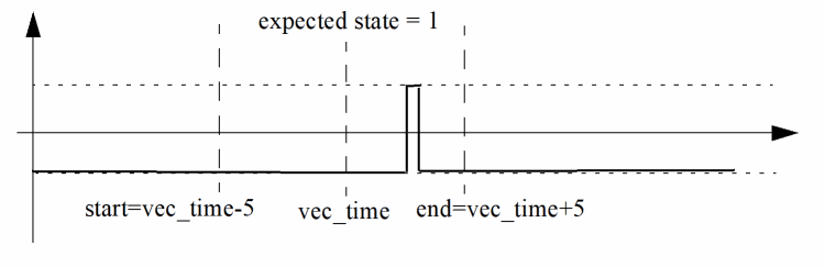
$timescale 1ns $end
.chkwindow 5 5 0
The .chkwindow statement is set to 0, so the waveform passes the vector check (see Figure E-1).
Figure E-1 Vector Check with .chkwindow Set to 0
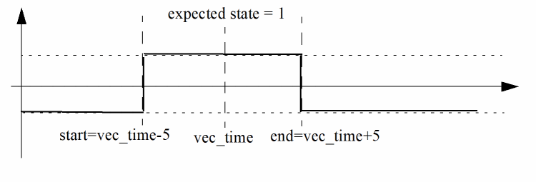
$timescale 1ns $end
.chkwindow 5 5 1
The .chkwindow is statement set to 1 and the signal remains at that state for the entire window period, in order to pass the vector check (see Figure E-2). If the signal matches Figure E-1, the vector check fails.
Figure E-2 Vector Check with .chkwindow Set to 1
$timescale 100ps $end
.chkwindow 5 5 1 period=100 first=20 p[*] out_*
tells the simulator to activate periodic window checking for signals p[*] and out_*. The vector check points start at 2 ns and repeats every 10 ns.
.hier 1
.chkwindow 5 5 1 first=20 X1.Xana.p[*] X1.Xdigital.Xcore.out_*
tells the simulator to ignore the first argument because a valid period argument has not been specified. The other arguments are used in the simulation.
Signal Timing
The signal timing characteristics (delay, rise and fall time) are defined in this section.
.trise and .tfall. statements are reasonable (warning message is issued when the defined value is too small or large)..idelay
.idelay time_value [signal_name1 ... signal_nameN]
Description
The .idelay statement specifies the delay time for the corresponding input signals. If a bidirectional signal is specified, this only applies to the input stage of the bidirectional signal. The default value is 0.0, if .idelay and .tdelay are not set.
Example
$timescale 1ns $end
.idelay 5
All input signals have a time delay of 5 ns.
$timescale 100 ps $end
.hier 1
.scope Xtop.XI1
.in a[0:3] b
.tdelay 0.1 Xtop.XI1.a* Xtop.XI1.b
The Xtop.XI1.a[0:3] and Xtop.XI1.b input signals have a delay time of 10 ps.
.odelay
.odelay time_value [signal_name1 ... signal_nameN]
Description
The .odelay statement specifies the delay time for the corresponding output signals. If a bidirectional signal is specified, this only applies to the output stage of the bidirectional signal. The default value is 0.0, if .odelay and .tdelay are not set.
Example
$timescale 1ns $end
.odelay 5
All output signals have a time delay of 5 ns.
.tdelay
.tdelay time_value [signal_name1 ... signal_nameN]
Description
The .tdelay statement specifies the delay time for the corresponding input, output, and bidirectional signals. The default value is 0.0, if .tdelay, .idelay, and .odelay are not specified.
Example
$timescale 1ns $end
.tdelay 5
All signals have a time delay of 5 ns.
.tfall
.tfall time_value [signal_name1 ... signal_nameN ]
Description
The .tfall statement specifies the fall time of the input signal. If .tfall is not specified, the default value is 0.1 n.
Examples
$timescale 1 ns $end
.tfall 0.1
all input signals have a fall time of 0.1 ns.
$timescale 1 ns $end
.in a[0:3] b
.tfall 0.1 a[0:3] b
input signals a[0:3] and b have a fall time of 0.1 ns.
.trise
.trise time_value [signal_name1 ... signal_nameN]
Description
The .trise statement specifies the rise time of the input signal. If .trise is not specified, the default value is 0.1 n.
Examples
$timescale 1 ns $end
.trise 0.1
all input signals have a rise time of 0.1 ns.
$timescale 1 ns $end
.in a[0:3] b
.trise 0.1 a[0:3] b
input signals a[0:3] and b have a rise time of 0.1 ns.
Voltage Threshold
As digital vector format, the voltage threshold for logic low and high can be specified using the following statements to convert the input vectors to stimuli or to perform an output vector check.
.vih
.vih voltage_value [signal_name1 ... signal_nameN]
Description
The .vih statement specifies the logic high voltage of the input signal. If .vih is not specified, the default voltage is 3.3.
You can also use a parameter name to specify the voltage. For example:
.vih pwr_vdd
The .vih statement also supports global and local specifications as well as expressions, as shown below.
.vih pwr_vdd
.vih pwr_vdd_cpu_sram r*cpu_sram[*]
.vih pwr_vdd *.08
Examples
.vih 5.0
tells Spectre all input signals have a logic high voltage of 5.0.
.in a[0:3] b
.vih 5.0 a[*] b
tells the simulator input signals a[0:3] and b have a logic high voltage of 5.0.
.vil
.vil voltage_value [signal_name1 ... signal_nameN]
Description
The .vil statement specifies the logic low voltage of the input signal. If .vil is not specified, the default voltage is 0.0.
Like vil also support parameters, global and local specifications, and expressions.
Examples
.vil 1.0
tells Spectre all input signals have a logic low voltage of 1.0.
.in a[0:3] b
.vil 1.0 a[0:3] b
tells the simulator input signals a[0:3] and b have a logic low voltage of 1.0.
.voh
.voh voltage_value [ signal_name1 ... signal_nameN ]
Description
The .voh statement specifies the logic high voltage of signals defined as outputs and signals from the analog netlist file that are used in the signal information file. If .voh is not specified, the default voltage is 3.3.
Like .vih, .voh also support parameters, global and local specifications, and expressions.
Examples
.voh 5.0
tells Spectre that all output signals have a logic high voltage of 5.0.
.out out[0:3] outA
.voh 5.0 out[*] outA
tells the simulator output signals out[0:3] and outA have a logic high voltage of 5.0.
.vol
.vol voltage_value [signal_name1 ... signal_nameN]
Description
The .vol statement specifies the logic low voltage of signals defined as outputs and signals from the analog netlist file that are used in the signal information file. If .vol is not specified, the default voltage is 0.0.
Like .vih, .vol also support parameters, global and local specifications, and expressions.
Examples
.vol 1.0
tells Spectre that all output signals have a logic low voltage of 1.0.
.out out[0:3] outA
.vol 1.0 out[0:3] outA
tells the simulator output signals out[*] and outA have a logic low voltage of 1.0.
Driving Ability
For input stimuli, the output resistance of VCD/EVCD sources can affect Spectre results. To specify the driving ability of VCD/EVCD sources, use the following statements:
.outz
.outzresistance [signal_name1 ... signal_nameN]
Description
The .outz statement specifies the output resistance for corresponding input signals. If .outz is not specified, the default value is 0.01.
Example
.outz 1meg
All input signals have an output resistance of 1 Megaohm.
.triz
.trizresistance [signal_name1 ... signal_nameN]
Description
The .triz statement specifies the output impedance when the corresponding input signals are in tri-state. If .triz is not specified, the default value is 1,000 Meg.
Example
.triz 500meg
All input signals have an output impedance of 500 Megaohms.
Hierarchical Signal Name Mapping
Hierarchical signal name mapping can be used to precisely match signals between the VCD and analog netlist files, and is defined by Spectre hier statement:
.hier 0 | 1
The .hier statement is used to specify hierarchical names in both the VCD and analog netlist files.
The key differences between flat and hierarchical mapping include:
-
To match hierarchical signals in the VCD file, the complete hierarchical structure needs to be specified in the
.scope,.alias, and.chkwindowstatements, as well as in the signal characteristic statements. For flat mapping, only the signal names are needed. -
For hierarchical signal name mapping, the statements to define the port direction of the signal are related to the
.scopestatement, which includes the.in,.out, and.bistatements. When using flat mapping, the multiple scopes defined by the.scopestatement are regarded as set. Spectre searches all of the scopes to perform a signal match and outputs an error message when the same signal name is defined in more than one VCD scope. -
The hierarchical structure of the analog netlist file is specified by the
.aliasstatement when performing hierarchical mapping.
Enhanced Statements
.scope and .in/.out/.bi
When using Spectre to apply hierarchical names to the VCD/EVCD and analog netlist files (.hier 1), the hierarchical structure in the VCD/EVCD file must be clearly defined with the .scope statement. The .in, .out, and .bi statements are used to define the signal name in the specified .scope statement and cannot contain the hierarchical structure. For the .bi statement, the enable signal needs to contain the hierarchical path because the signal may belong to a different scope.
The VCD/EVCD signal info file supports multiple .scope statements. The effective scope of each .scope statement is affected by the other statements, requiring the .in, .out, and .bi statements to be in the correct location.
$scope module top $end
$scope module digital $end
$var reg 1 ! din_1 $end
$var reg 1 " en $end
$scope module drv $end
$var reg 1 ! mid[1] $end
$var reg 1 " inout $end
$upscope $end
$upscope $end
$upscope $end
.hier 1
.scope top.digital
* The effective scope is top.digital
.in din_1 en
* The scope top.digital is ended by the next .scope statement
.scope top.digital.drv
* The effective scope is changed to top.digital.drv
.out mid[*]
.bi top.digital.en inout
.alias
.alias targ_signame alias_signame
The hierarchical structures that are defined in the .scope statement are used only for the VCD/EVCD file, so the .alias statement is needed to map the signals to the lower circuit levels of the analog netlist file.
.alias statements define the mapping relationship for a signal, the last .alias statement is used by the simulator, and the other statements are overwritten..alias TOP.module1.in1 X1.in1
.scope Top.module1
.in in1
tells Spectre to map the TOP.module1.in1 defined in the .scope and .in/.out/.bi statements to the signal in1 of instance X1 in the analog netlist file.
.alias *[*] *<*>
.alias Top.module1.sig_*[*] X1.vec_*<*>
.scope Top.module1
.out sig_[0:15]
.scope digital_block
.in datain[*]
tells the simulator for the Top.module1.sig_[0:15] signals, the second .alias statement overwrites the first .alias statement and maps the signals to X1.vec_<0>, ... X1.vec_<15>. Since only the first .alias statement matches the digital_block.datain[*] signals, they are mapped to digital_block.datain<*> of the analog netlist file.
-
Analog netlist file:
Opt options hier_delimiter = %
-
VCD/EVCD info file:
.alias TOP.module1.sig_[*] X1%Xdrv%vec_<*>
.scope Top.module1
.out sig_*
Hierarchical Signal Names
For hierarchical mapping, the signal names in the .alias and .chkwindow statements, as well as in the signal characteristic statements, must have the hierarchical structure in the VCD file.
.hier 1
.chkwindow -1 5 1 Top.X1.out*
.vih 1.2 X1.in[*]
.vol 0.2 X1.dout1 Xdig.X2.dout1
.tfall 0.2 Xana.X1.in* Xdig.din*
.outz 100 X1.in[*]
Enhanced VCD Commands
Since the EVCD and VCD formats are similar, only the key EVCD format differences will be discussed in this section:
Signal Strength Levels
Verilog HDL allows scalar net signal values to have a full range of unknown values, and different levels of strength or combinations of levels of strength. For logic operation, multiple-level logic strength modeling resolves combinations of signals into known or unknown values, allowing the behavior of hardware to be represented with improved accuracy.
EVCD signal strength can be defined by eight values, ranging from 0 (weakest) to 7 (strongest). The most commonly used values are 0 and 6. For example, for logic value 0
<0_strength_component> =6 , <1_strength_component> =0
<0_strength_component> =0 , <1_strength_component> =6
Spectre ignores the strength information (minimal impact on most CMOS circuit designs). If you want to preserve driver strength during simulation, specify .outz in the signal information file for specific signals with different output resistances.
For more information about logic strength modeling, refer to IEEE Std 1364-2001.
Value Change Data Syntax
The EVCD data command is different from the one used with VCD because the EVCD version can provide strength information and additional signal states.
data
p[port_value] [0_strength_component] [1_strength_component] [identifier_code]
Description
The value change section shows the actual value changes at each simulation time increment. Only variables that change value during a time increment are listed. In the EVCD file, strength information and a larger number of value states with port direction are presented in the value change section. The arguments for the EVCD data command are listed below.
Arguments
|
State character which contains information about driving direction and the value of the port. The state characters are described in “Port Direction and Value Mapping” (see tables). |
|
|
One of the eight Verilog strength values indicating the |
|
|
One of the eight Verilog strength values indicating the |
|
|
The identifier code for the port, which is defined in the $var construct for the port. |
Examples
pU 0 7 <0
tells Spectre that one bit bus with identifier <0 (defined by $var) has a binary value of U, and the strength of 0 component is 0 and the strength of 1 component is 7.
pCCC 667 667 !
tells the simulator the bus with identifier ! (defined by $var) has a binary value of CCC, and the strength of 0 component is 667 and the strength of 1 component is 667. There is more than one driver on this port and the resolved value is CCC.
Port Direction and Value Mapping
The port value in the EVCD file contains port direction information, which helps Spectre distinguish some of the x states, apply stimuli for input signals, or perform a vector check for output signals.
input Direction
Given an DUT and a test fixture, the driving direction is input if the text fixture drivers are driving a non-tristate value and the drivers inside the DUT are tri-state. The resolved value is mapped in Table E-6.
When reading the mapping information in the following tables, it is important to note:
-
Declared
inand declaredoutindicates the signal is defined asinputandoutputin the signal information file. The termactiveimplies the drivers are in a non-tristate condition. -
Because the conflicting states of the signal value are converted to
xin the VCD file, they are regarded as “not needed” and Spectre does not perform a vector check when the signals are specified asoutput. -
Combining the port direction for the signal value in the EVCD file and the specified direction in the signal information file, Spectre can distinguish the
inputandoutputvalues of a signal and perform a vector check when it is specified asoutputin the signal information file.
output Direction
The driving direction is output if the driving value from drivers inside the DUT is non-tristate, but the value driven by the drivers in the test fixture is tri-state. The resolved value is mapped in Table E-7.
unknown Direction
The driving direction is unknown if both the drivers in the test fixture and DUT are driving a non-tristate value. The resolved value is mapped in Table E-8.
| Port Value | Declared in | Declared out | Declared bi Enable = 0 | Declared bi Enable = 1 | Mapped VCD Value |
|---|---|---|---|---|---|
Enhanced VCD Format Example
The following is an example of EVCD file format.
$date
Jul 11, 2004 15:42:26
$end
$version
TOOL: ncsim 05.00-p001
$end
$timescale
1 ns
$end
$scope module board $end
$scope module counter $end
$var port [3:0] ! value $end
$var port 1 clock $end
$var port 1 # fifteen $end
$var port 1 $ altFifteen $end
$upscope $end
$upscope $end
$enddefinitions $end
#0
$dumpports
pXXXX 6666 6666 !
pN 6 6 "
pX 6 6 #
pX 6 6 $
$end
#5
pU 0 6 "
#10
pLLLL 6666 0000 !
pL 6 0 #
pL 6 0 $
#50
pD 6 0 "
...
Frequently Asked Questions
- Is it necessary to modify the VCD/EVCD file to match the signals?
- How can I verify the input stimuli?
- How do I verify the output vector check?
- Why should I use hierarchical signal name mapping?
- What is the difference between CPU and user time?
Is it necessary to modify the VCD/EVCD file to match the signals?
You can adjust the signal information file to match signals in the VCD/EVCD file with those in the netlist file, and leave the VCD/EVCD file unchanged. Spectre only needs the scopes specified in the .scope statement and ignores the other scopes (the simulator also ignores the parent or child scope of the specified scope). The .alias statement can be used to map the signal names between the VCD/EVCD and circuit netlist files.
How can I verify the input stimuli?
As digital vector format, first probe the signals in the top-level using .probe tran v(*) depth=1 and check the waveform outputs with the Virtuoso Visualization and Analysis or SimVision viewers.
Review the log file to check if the signals defined in the digital vector file match those defined in the analog netlist file.
- If the signal is in the specified scope of VCD/EVCD, but not in the VCD info file, a warning message appears.
- If the signal is in the specified scope of VCD/EVCD and in the VCD info file, but not in the analog netlist file, a warning message appears.
- If the signal is in the analog netlist file, but does not match the one in VCD/EVCD, check the list of dangling nodes or no DC path to the ground.
How do I verify the output vector check?
A <netlistName>_<tranName>.veclog file is generated at the location specified by Spectre option-raw statement if there are any vector checks. A <netlistName>_<tranName>.vecerr file is also generated when errors occur during the vector check. Refer to these two files for detailed information about the vector check. Here, <netlistName> refers to the name of the netlist and <tranName> refers to the name of the transient analysis.
When the signal is defined in both the VCD/EVCD files and the VCD info file, but not in the analog netlist file, the simulator issues a warning message.
Why should I use hierarchical signal name mapping?
Flat signal name mapping works for most situations, but suffers from the following limitations:
- Only the signals in the top level can be mapped to the VCD file (analog netlist file).
-
When multiple
.scopestatements are used in a digital VCD file, Spectre treats them as a single set and searches for signals (as defined in the.in,.out, and.bistatements) in all of the.scopestatements. An error occurs when a signal with the same name appears in more than one.scopestatement.
Hierarchical signal name mapping is able to overcome these limitations, allowing you to map signals to the lower levels of the analog netlist file and to use multiple .scope statements (see “Enhanced Statements” for more information about .scope statements).
What is the difference between CPU and user time?
Description
- CPU time is the time the central processing unit (CPU) spends running the user program
- User time is the user and system times combined (that is, the total time needed to provide system service to the user program)
When running a simulation, Spectre stores the elapsed CPU and user time information in the STDOUT (standard output) or log file. The estimated completion time is based on linear interpolation of the user time from the start of the simulation. To view such information in STDOUT, set annotated=estimated in the tran statement.
Example
tran: time = 3.303 us    (82.6 %), step = 9.036 ps     (226 u%)
cpu = 957402.0 s, elapsed = 190995.8 s, steps = 144244, mem = 45959.8 MB
estimated completion time:  10:12:07
Return to top